Archive for the ‘Break IC’ Category
 Break Microcontroller PIC18F4220 Binary
 August 22nd, 2014 |
  Author:
 · Self-programmability: These devices can write to their own program memory spaces under internal software control. By using a bootloader routine located in the protected Boot Block at the top of program memory to Break Microcontroller PIC18F4220 Binary, it becomes possible to create an application that can update itself in the field.
· Enhanced CCP Module: In PWM mode, this module provides 1, 2 or 4 modulated outputs for controlling half-bridge and full-bridge drivers. Other features include Auto-Shutdown for disabling PWM outputs on interrupt or other select conditions and Auto-Restart to reactivate outputs once the condition has cleared.
Addressable USART: This serial communication module is capable of standard RS-232 operation using the internal oscillator block, removing the need for an external crystal (and its accompanying power requirement) in applications that talk to the outside world.
· 10-bit A/D Converter: This module incorporates programmable acquisition time, allowing for a channel to be selected and a conversion to be initiated without waiting for a sampling period and thus, reduce code overhead.
· Extended Watchdog Timer (WDT): This enhanced version incorporates a 16-bit prescaler, allowing a time-out range from 4 ms to over 2 minutes, that is stable across operating voltage and temperature.
The EC and ECIO Oscillator modes require an external clock source to be connected to the OSC1 pin. There is no oscillator start-up time required after a Power-on Reset or after an exit from Sleep mode. In the EC Oscillator mode, the oscillator frequency divided by 4 is available on the OSC2 pin. This signal may be used for test purposes or to synchronize other logic by Break Microcontroller PIC18F4220 Binary.
For timing insensitive applications, the “RC” and “RCIO” device options offer additional cost savings. The RC oscillator frequency is a function of the supply voltage, the resistor (REXT) and capacitor (CEXT) values and the operating temperature.
In addition to this, the oscillator frequency will vary from unit to unit due to normal manufacturing variation. Furthermore, the difference in lead frame capacitance between package types will also affect the oscillation frequency, especially for low CEXT values.
The user also needs to take into account variation due to tolerance of external R and C components used. Figure 2-6 shows how the R/C combination is connected. In the RC Oscillator mode, the oscillator frequency divided by 4 is available on the OSC2 pin. This signal may be used for test purposes or to synchronize other logic.
Break IC GAL22V10D-10LJ Binary
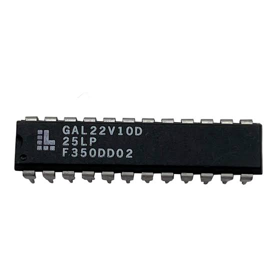
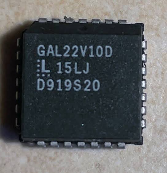
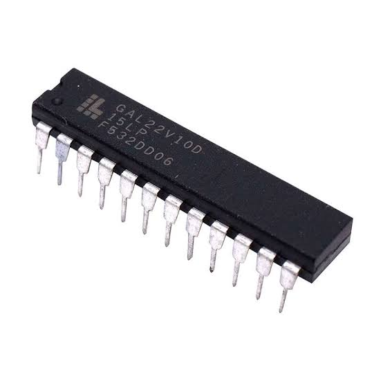
The GAL22V10D-10LJ is a classic Programmable Logic Device (PLD) from Lattice Semiconductor, widely deployed in automotive engine control units, industrial automation controllers, telecommunications infrastructure, medical instrumentation, and military avionics. Unlike a standard microcontroller, this chip contains a embedded logic array that implements custom firmware – typically in the form of binary logic equations rather than source code.
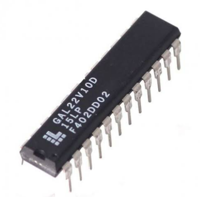
Its key features include 10 macrocells, 22 inputs, high-speed operation (10 ns propagation delay), and a protective security fuse that, when locked, prevents any readout of the internal data. Many legacy systems still rely on this PLD because of its reliability and low power consumption. However, when the original design file or heximal program is lost, the secured memory becomes an inaccessible archive that threatens the entire product’s maintainability.
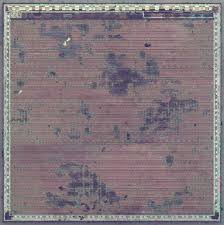
Break IC GAL22V10D-10LJ Binary from its memory and rewrite the program into new PLD GAL22V10D:
HIGH PERFORMANCE E2CMOS® TECHNOLOGY
— 4 ns Maximum Propagation Delay
— Fmax = 250 MHz
— 3.5 ns Maximum from Clock Input to Data Output
— UltraMOS® Advanced CMOS Technology which has been fully developed in the process of Break IC GAL22V10D-10LJ Binary
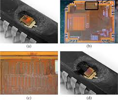
The need to break into a locked GAL22V10D arises when equipment becomes obsolete and the original source code or binary file no longer exists. Without the ability to retrieve the internal firmware, a failed chip would scrap expensive machinery. To hack this PLD, one must first decapsulate the plastic package using chemical or laser techniques, then physically probe the embedded memory cells or exploit timing faults to decode the encrypted logic pattern. The goal is to clone or duplicate the exact program into a new device. The protective security fuse on the GAL22V10D is designed to block standard programmers from performing a readout. Thus, a direct attack is impossible without invasive methods. Our service specializes in this break process:
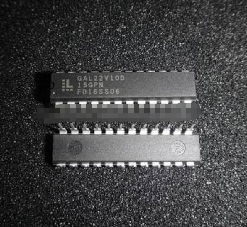
we decapsulate the chip, retrieve the binary data from the flash-equivalent cells, and produce a complete heximal file that mirrors the original firmware. This archive can then be cloned into fresh PLD units, restoring full functionality.
· ACTIVE PULL-UPS ON ALL PINS
· COMPATIBLE WITH STANDARD 22V10 DEVICES
— Fully Function/Fuse-Map/Parametric Compatible with Bipolar and UVCMOS 22V10 Devices
· 50% to 75% REDUCTION IN POWER VERSUS BIPOLAR
— 90mA Typical Icc on Low Power Device
— 45mA Typical Icc on Quarter Power Device
· E2 CELL TECHNOLOGY
— Reconfigurable Logic
— Reprogrammable Cells
— 100% Tested/100% Yields
— High Speed Electrical Erasure (<100ms)
— 20 Year Data Retention
· TEN OUTPUT LOGIC MACROCELLS
— Maximum Flexibility for Complex Logic Designs
Our break procedure follows a disciplined workflow. First, we chemically decapsulate the protected GAL22V10D without damaging the silicon die. Next, using micro‑probing stations, we decode the locked logic configuration stored in the EEPROM‑like cells. The extracted binary is then verified against the original chip’s behavior. Finally, we deliver a heximal file that can be programmed into any compatible PLD – effectively allowing you to clone or duplicate the program for unlimited replacements. The benefits for our clients are substantial: you avoid costly system redesigns, extend the life of obsolete equipment, and regain control over your embedded firmware. Whether you need to retrieve a lost archive, clone a failing chip, or simply decode a secured logic pattern for reverse engineering, our service delivers a clean, reliable binary output.
· PRELOAD AND POWER-ON RESET OF REGISTERS
— 100% Functional Testability
· APPLICATIONS INCLUDE:
— DMA Control
— State Machine Control
— High Speed Graphics Processing
— Standard Logic Speed Upgrade
· ELECTRONIC SIGNATURE FOR IDENTIFICATION
The GAL22V10, at 4ns maximum propagation delay time, combines a high performance CMOS process with Electrically Erasable (E2) floating gate technology to provide the highest performance available of any 22V10 device on the market.
CMOS circuitry allows the GAL22V10 to consume much less power when compared to bipolar 22V10 devices. E2 technology offers high speed (<100ms) erase times, providing the ability to reprogram or reconfigure the device quickly and efficiently which is critical for Break IC GAL22V10D-10LJ Binary.
The generic architecture provides maximum design flexibility by allowing the Output Logic Macrocell (OLMC) to be configured by the user. The GAL22V10 is fully function/fuse map/parametric compatible with standard bipolar and CMOS 22V10 devices.
Unique test circuitry and reprogrammable cells allow complete AC, DC, and functional testing during manufacture. As a result, Lattice Semiconductor delivers 100% field programmability and functionality of all GAL products. In addition, 100 erase/write cycles and data retention in excess of 20 years are specified.
We offer confidential, fast, and precise break services for the GAL22V10D-10LJ and many other PLD families. Every attack is performed with care to preserve the data integrity. Contact us with your locked chip, and we will decapsulate, decode, and retrieve the complete binary file – turning a protected memory into a usable archive for production.
Break Microcontroller MSP430F4361 Software
Break Microcontroller MSP430F4361 Software
MSP430 Microcontrollers (MCUs) from Texas Instruments (TI) are 16-bit, RISC-based, mixed-signal processors designed specifically for ultra-low-power. MSP430 MCUs have the right mix of intelligent peripherals, ease-of-use, low cost and lowest power consumption for thousands of applications which makes it becomes popular to Break Microcontroller MSP430F4361 Software.
TI offers robust design support for the MSP430 MCU platform along with technical documents, training, tools and software to help designers develop products and release them to market faster.
MSP430 Microcontroller DNA
Ultra-Low Power
The MSP430 MCU is designed specifically for ultra-low-power applications. Its flexible clocking system, multiple low-power modes, instant wakeup and intelligent autonomous peripherals enable true ultra-low-power optimization, dramatically extending battery life.
Flexible Clocking System – The MSP430 MCU clock system has the ability to enable and disable various clocks and oscillators which allow the device to enter various low-power modes (LPMs). The flexible clocking system optimizes overall current consumption by only enabling the required clocks when appropriate.
Multiple-Oscillator Clock System
Key Features
· Integrated intelligent peripherals including a wide range of high-performance analog and digital peripherals that off-load the CPU
· Easy-to-use 16-bit RISC CPU architecture enables new applications with industry-leading code density.
· Complete development ecosystem with tools starting at $4.30
400+ Ultra-Low-Power Devices
8-MHz to 25-MHz CPU Speed
0.5KB to 256KB Flash
128B to 18KB RAM
14 to 113 pins; 25+ packages
Sub-Main Clock (SMCLK) – Source for faster individual peripheral modules that may be driven by the internal DCO up to 25 MHz or with external crystal.
Instant Wakeup – The MSP430 MCU can wake-up instantly from LPMs. This ultra-fast wake-up is enabled by the MSP430 MCU’s internal digitally controlled oscillator (DCO), which can source up to 25 MHz and be active and stable in 1µs. Instant wake-up functionality is important in ultra-low-power applications since it allows the microcontroller to use the CPU in very efficient bursts and spend more time in LPMs and provide a better chance to Break Microcontroller MSP430F4361 Software.
Zero-Power Brown-Out Reset (BOR) – The MSP430 MCU’s BOR is always enabled and active in all modes of operation.
the most reliable performance possible while maintaining ultra-low-power consumption. The BOR circuit detects low supply voltages and Lower-Power Peripherals resets the device when power is applied or removed. This functionality is especially critical in battery-powered applications.
Break MCU PIC16C717 Program
We can Break MCU PIC16C717 Program, please view the MCU PIC16C717 features for your reference:
MCU Core Features:
· High-performance RISC CPU
· Only 35 single word instructions to learn
· All single cycle instructions except for program branches which are two cycle
· Operating speed: DC – 20 MHz clock input
· Interrupt capability (up to 10 internal/external interrupt sources)
· Eight level deep hardware stack
· Direct, indirect and relative addressing modes
· Power-on Reset (POR)
· Power-up Timer (PWRT) and Oscillator Start-up Timer (OST)
· Watchdog Timer (WDT) with its own on-chip RC oscillator for reliable operation
· Selectable oscillator options:
– INTRC – Internal RC, dual speed (4MHz and 37KHz) dynamically switchable for power savings and Break MCU PIC16C717 Program
– ER – External resistor, dual speed (user selectable frequency and 37KHz) dynamically switchable for power savings
– EC – External clock
– HS – High speed crystal/resonator
– XT – Crystal/resonator
– LP – Low power crystal
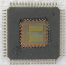
Break MCU PIC16C717 Program
· Low-power, high-speed CMOS EPROM technology
· In-Circuit Serial Programming™ (ISCP)
· Wide operating voltage range: 2.5V to 5.5V
· 15 I/O pins with individual control for:
– Direction (15 pins)
– Digital/Analog input (6 pins)
– PORTB interrupt on change (8 pins)
– PORTB weak pull-up (8 pins)
– High voltage open drain (1 pin)
· Commercial and Industrial temperature ranges
· Low-power consumption:
– < 2 mA @ 5V, 4 MHz
– 22.5 µA typical @ 3V, 32 kHz
· Timer0: 8-bit timer/counter with 8-bit prescaler
· Timer1: 16-bit timer/counter with prescaler, can be incremented during sleep via external crystal/clock
· Timer2: 8-bit timer/counter with 8-bit period register, prescaler and postscaler
· Enhanced Capture, Compare, PWM (ECCP) module
– Capture is 16 bit, max. resolution is 12.5 ns
– Compare is 16 bit, max. resolution is 200 ns
– PWM max. resolution is 10 bit
– Enhanced PWM:
– Single, Half-Bridge and Full-Bridge output modes by Break MCU PIC16C717 Program
– Digitally programmable deadband delay
· Analog-to-Digital converter:
– PIC16C770/771 12-bit resolution
– PIC16C717 10-bit resolution
· On-chip absolute bandgap voltage reference generator
· Programmable Brown-out Reset (PBOR) circuitry
· Programmable Low-Voltage Detection (PLVD) circuitry
· Master Synchronous Serial Port (MSSP) with two modes of operation:
– 3-wire SPI™ (supports all 4 SPI modes)
– I2C™ compatible including master mode support only
· Program Memory Break (PMR) capability for look-up table, character string storage and checksum calculation purposes
Break Microcontroller PIC16C716 Heximal
There are two memory blocks in each of these PICmicro® microcontroller devices. Each block (Program Memory and Data Memory) has its own bus so that concurrent access can occur which provide necessity for Break Microcontroller PIC16C716 Heximal.
The PIC16C712/716 has a 13-bit program counter capable of addressing an 8K x 14 program memory space. PIC16C712 has 1K x 14 words of program memory and PIC16C716 has 2K x 14 words of program memory. Accessing a location above the physically implemented address will cause a wraparound.
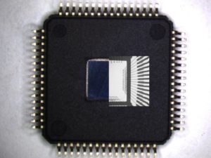
Break Microcontroller PIC16C716 Heximal
The reset vector is at 0000h and the interrupt vector is at 0004h.
Each bank extends up to 7Fh (128 bytes). The lower locations of each bank are reserved for the Special
Function Registers. Above the Special Function Registers are General Purpose Registers, implemented as static RAM. All implemented banks contain special function registers. Some “high use” special function registers from one bank may be mirrored in another bank for code reduction and quicker access.
The Special Function Registers are registers used by the CPU and Peripheral Modules for controlling the desired operation of the device.
The special function registers can be classified into two sets; core (CPU) and peripheral. Those registers associated with the core functions are described in detail in this section. Those related to the operation of the peripheral features are described in detail in that peripheral feature section.
The STATUS register, shown in Figure 2-4, contains the arithmetic status of the ALU, the RESET status and the bank select bits for data memory in the process of Break Microcontroller PIC16C716 Heximal. The STATUS register can be the destination for any instruction, as with any other register.
If the STATUS register is the destination for an instruction that affects the Z, DC or C bits, then the write to these three bits is disabled. These bits are set or cleared according to the device logic. Furthermore, the TO and PD bits are not writable. Therefore, the result of an instruction with the STATUS register as destination may be different than intended.
The program counter (PC) specifies the address of the instruction to fetch for execution. The PC is 13 bits wide. The low byte is called the PCL register after Break Microcontroller. This register is readable and writable. The high byte is called the PCH register. This register contains the PC<12:8> bits and is not directly readable or writable. All updates to the PCH register go through the PCLATH register.
The stack allows a combination of up to 8 program calls and interrupts to occur. The stack contains the return address from this branch in program execution. Midrange devices have an 8 level deep x 13-bit wide hardware stack. The stack space is not part of either program or data space and the stack pointer is not readable or writable. The PC is PUSHed onto the stack when a CALL instruction is executed or an interrupt causes a branch. The stack is POPed in the event of a RETURN, RETLW or a RETFIE instruction execution.
PCLATH is not modified when the stack is PUSHed or POPed.
After the stack has been PUSHed eight times, the ninth push overwrites the value that was stored from the first push. The tenth push overwrites the second push (and so on).
 Posted in Break IC |
  Tags: copia cip eeprom, copia circuite integrate program, copia ic archive, copia mcu dump, copia microcontroler firmware, lovi cip hex, lovi circuite integrate code, lovi ic software, lovi mcu bin, lovi microcontroler flash |
  Comments Closed
Break Chip PALCE16V8 Software
The Cypress PALCE16V8 is a CMOS Flash Electrical Erasable second-generation programmable array logic device. It is implemented with the familiar sum-of-product (AND-OR) logic structure and the programmable macrocell which is easier to Break Chip PALCE16V8 Software.
Functional Description (continued)
The PALCE16V8 is executed in a 20-pin 300-mil molded DIP, a 300-mil cerdip, a 20-lead square ceramic leadless chip car-
rier, and a 20-lead square plastic leaded chip carrier. The device provides up to 16 inputs and 8 outputs. The PALCE16V8 can be electrically erased and reprogrammed. The programmable macrocell enables the device to function as a superset to the familiar 20-pin PLDs such as 16L8, 16R8, 16R6, and 16R4.
The PALCE16V8 features 8 product terms per output and 32 input terms into the AND array. The first product term in a macrocell can be used either as an internal output enable control or as a data product term.
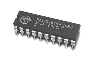
Break Chip PALCE16V8 Software
There are a total of 18 architecture bits in the PALCE16V8 macrocell; two are global bits that apply to all macrocells and 16 that apply locally, two bits per macrocell.
The architecture bits determine whether the macrocell functions as a register or combinatorial with inverting or noninverting output. The output enable control can come from an external pin or internally from a product term.
The output can also be permanently enabled, functioning as a dedicated output or permanently disabled, functioning as a dedicated input. Feedback paths are selectable from either the input/output pin associated with the macrocell, the input/output pin associated with an adjacent pin, or from the macrocell register itself to Break Chip PALCE16V8 Software.
Configuration Table
Power-Up Reset
All registers in the PALCE16V8 power-up to a logic LOW for predictable system initialization. For each register, the associated output pin will be HIGH due to active-LOW outputs.
Electronic Signature
An electronic signature word is provided in the PALCE16V8 that consists of 64 bits of programmable memory that can contain user-defined data.
Security Bit
A security bit is provided that defeats the readback of the internal programmed pattern when the bit is programmed.
Low Power
Product Term Disable
Product Term Disable (PTD) fuses are included for each product term. The PTD fuses allow each product term to be individually disabled.
Posted in Break IC |
Tags: вырваться ic archive, вырваться mcu dump, вырваться интегральная схема flash, вырваться микроконтроллер eeprom, вырваться чип flash, ломаться ic firmware, ломаться mcu bin, ломаться интегральная схема hex, ломаться микроконтроллер code, ломаться чип program |
Comments Closed
Break IC XC9572-15PQ100C Binary
We can Break IC XC9572-15PQ100C Binary, below IC XC9572-15PQ100C features for your reference:
Features
7.5 ns pin-to-pin logic delays on all pins fCNT to 125 MHz
72 macrocells with 1,600 usable gates
Up to 72 user I/O pins
5V in-system programmable
Product Specification
Description
The XC9572 is a high-performance CPLD providing advanced in-system programming and test capabilities for general purpose logic integration which is one of the main reasons for its popularity of Break IC XC9572-15PQ100C Binary. It is comprised of eight 36V18 Function Blocks, providing 1,600 usable gates with propagation delays of 7.5 ns. See Figure 2 for the architecture overview.
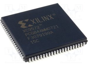
Break IC XC9572-15PQ100C Binary
– Endurance of 10,000 program/erase cycles
– Program/erase over full commercial voltage and temperature range
Enhanced pin-locking architecture
Flexible 36V18 Function Block
– 90 product terms drive any or all of 18 macrocells within Function Block
– Global and product term clocks, output enables, set and reset signals
Extensive IEEE Std 1149.1 boundary-scan (JTAG) support
Programmable power reduction mode in each macrocell
Slew rate control on individual outputs
User programmable ground pin capability
Extended pattern security features for design protection
High-drive 24 mA outputs
3.3V or 5V I/O capability
Advanced CMOS 5V FastFLASH™ technology
Supports parallel programming of more than one
XC9500 concurrently
Available in 44-pin PLCC, 84-pin PLCC, 100-pin PQFP, and 100-pin TQFP packages
Power Management
Power dissipation can be reduced in the XC9572 by configuring macrocells to standard or low-power modes of operation. Unused macrocells are turned off to minimize power dissipation when Break IC XC9572-15PQ100C Binary.
ICC (mA) = MCHP (1.7) + MCLP (0.9) + MC (0.006 mA/MHz) f
Where:
MCHP = Macrocells in high-performance mode
MCLP = Macrocells in low-power mode
MC = Total number of macrocells used f = Clock frequency (MHz)
Posted in Break IC |
Tags: brechen chip software, brechen ic eeprom, brechen integrierte Schaltung code, brechen mcu flash, brechen Mikrocontroller firmware |
Comments Closed
Break CPLD EPM7064LC68-15 Binary
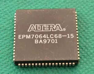
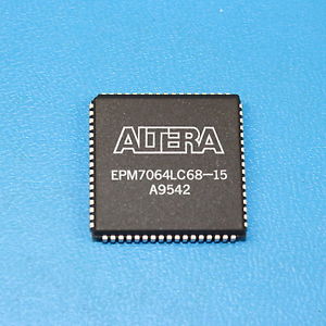
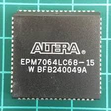
The EPM7064LC68-15 is a classic yet powerful PLD device widely utilized in legacy and long-lifecycle embedded systems. Known for its stable architecture and predictable timing behavior, this CPLD is commonly found in industrial automation controllers, telecommunications backplanes, medical devices, and defense-related electronics. It serves as a critical component for glue logic, interface management, and control sequencing, storing essential program structures and operational data within its internal memory. In most real-world deployments, the firmware, binary, or heximal configuration file inside the chip is intentionally protected, locked, or encrypted, making it extremely difficult to access the original source code or recover the design archive without specialized expertise.
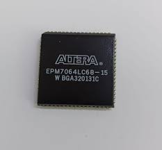
Our “Break CPLD EPM7064LC68-15 Binary” service focuses on advanced methodologies to attack, break, and decode these secured devices and recover critical embedded assets. Through a combination of precision decapsulate procedures and signal-level analysis, we are able to retrieve internal memory content, including firmware, structured binary streams, and heximal representations. Even when the device is heavily protected or encrypted, our approach allows us to effectively hack through the security layers and extract usable data. Once the raw file archive is obtained, we reconstruct the program logic into interpretable source code, enabling clients to clone, duplicate, or redeploy the original CPLD configuration. This process ensures that valuable intellectual property stored in flash-like structures or EEPROM-equivalent memory is not permanently lost.
Features
High-performance, EEPROM-based programmable logic devices (PLDs) based on second-generation MAX® architecture 5.0-V in-system programmability (ISP) through the built-in.
IEEE Std. 1149.1 Joint Test Action Group (JTAG) interface available in MAX 7000S devices
– ISP circuitry compatible with IEEE Std. 1532 before Break CPLD
Includes 5.0-V MAX 7000 devices and 5.0-V ISP-based MAX 7000S devices
Built-in JTAG boundary-scan test (BST) circuitry in MAX 7000S devices with 128 or more macrocells if Break CPLD
Complete EPLD family with logic densities ranging from 600 to 5,000 usable gates (see Tables 1 and 2) 5-ns pin-to-pin logic delays with up to 175.4-MHz counter frequencies (including interconnect) by Break CPLD EPM7064LC68-15 Binary.
PCI-compliant devices available
Altera Corporation
DS-MAX7000-6.7
For information on in-system programmable 3.3-V MAX 7000A or 2.5-V
MAX 7000B devices, see the MAX 7000A Programmable Logic Device Family
Data Sheet or theMAX 7000B Programmable Logic Device Family Data Sheet.
Circuit Engineering Company Limited continues to be recognized as the Southern China Leader in Services for IC Break, MCU RECOVER, Chip Recover, Microcontroller Copy service. With the advancement of today’s modern circuit board technology, it is more important than ever to have specialists available to help you at a moment’s notice.
Our engineering and commercial teams collectively have a vast amount of electronic experience covering field include Consumer Electronics, Industrial Automation Electronics, Wireless Communication Electronics., etc. For more information please contact us through email.
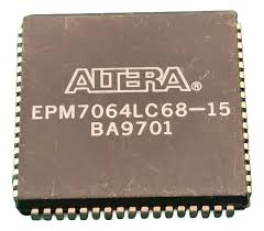
From a technical standpoint, the workflow integrates both invasive and non-invasive techniques. The decapsulation stage exposes the silicon die, allowing direct probing and facilitating deeper retrieval of embedded data. Complementing this, our proprietary tools perform logical decode operations on the extracted binary, converting fragmented data files into a coherent archive. This enables accurate reconstruction of the original firmware and program environment. By systematically breaking protection mechanisms and validating each stage of the data retrieval process, we deliver reliable outputs that can be directly used for engineering analysis, redesign, or replication. The result is not just raw memory dumps, but a refined and structured dataset ready for immediate application.
The practical value of this service is significant for organizations dealing with obsolete components, missing documentation, or the need for product continuity. By choosing to attack, decode, and recover secured CPLD data, clients gain full visibility into previously inaccessible firmware and source code, allowing them to maintain, upgrade, or clone existing systems without redesigning from scratch. This reduces development risk, shortens lead times, and ensures long-term support for critical hardware platforms. Ultimately, our capability to break, retrieve, and duplicate the EPM7064LC68-15 binary empowers engineers with the tools needed to preserve and extend the lifecycle of complex electronic systems.
Break CPLD EPM3128ATC100-7 Software
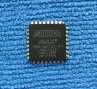
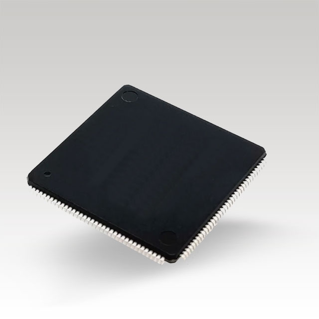
The EPM3128ATC100-7 is a widely used CPLD (Complex Programmable Logic Device) designed for high-reliability digital logic applications where deterministic timing and flexible logic configuration are required. Unlike traditional microcontrollers, this device implements hardware-defined logic rather than sequential firmware execution, making it ideal for industrial automation, telecom interfaces, automotive electronics, medical instrumentation, and embedded control systems. Its non-volatile memory structure allows configuration data to be retained without external storage, enabling stable long-term deployment. However, when original design archive, configuration file, or logic source code is lost, maintaining or reproducing the system becomes extremely difficult. The Break CPLD EPM3128ATC100-7 Software service is designed to recover and reconstruct this critical embedded logic data for authorized users.
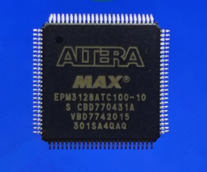
In many real-world applications, the EPM3128ATC100-7 is configured with protective, protected, locked, or encrypted security settings to prevent unauthorized access to its internal configuration memory. These protections secure the device’s program, binary, or heximal configuration data, making direct retrieval impossible through standard interfaces. Our service focuses on helping clients attack, break, or carefully decode these restrictions in a controlled engineering environment. By analyzing the embedded structure of the CPLD, we can retrieve configuration data, reconstruct the original logic program file, and rebuild usable archive outputs even when the device is fully secured. In advanced cases, controlled decapsulate techniques may be applied to access deeply embedded structures and extract configuration information from otherwise inaccessible memory regions. The goal is to recover consistent binary or heximal data that accurately represents the original device logic without compromising its integrity.
High–performance, low–cost CMOS EEPROM–based programmable logic devices (PLDs) built on a MAX® architecture 3.3-V in-system programmability (ISP) through the built–in IEEE Std. 1149.1 Joint Test Action Group (JTAG) interface with advanced pin-locking capability when Break CPLD EPM3128ATC100-7 Software.
– Enhanced ISP algorithm for faster programming
– ISP_Done bit to ensure complete programming
– Pull-up resistor on I/O pins during in–system programming
High–density PLDs ranging from 600 to 10,000 usable gates 4.5–ns pin–to–pin logic delays with counter frequencies of up to 227.3 MHz
MultiVoltTM I/O interface enabling the device core to run at 3.3 V, while I/O pins are compatible with 5.0–V, 3.3–V, and 2.5–V logic levels
Pin counts ranging from 44 to 256 in a variety of thin quad flat pack (TQFP), plastic quad flat pack (PQFP), plastic J–lead chip carrier (PLCC), and FineLine BGATM packages
Hot–socketing support
Programmable interconnect array (PIA) continuous routing structure for fast, predictable performance.
PCI compatible
Bus–friendly architecture including programmable slew–rate control
Open–drain output option
Programmable macrocell flipflops with individual clear, preset, clock, and clock enable controls
Programmable power–saving mode for a power reduction of over 50% in each macrocell
Configurable expander product–term distribution, allowing up to 32 product terms per macrocell
Programmable security bit for protection of proprietary designs which is necessary to be removed when Break CPLD EPM3128ATC100-7 Software
Enhanced architectural features, including:
– 6 or 10 pin– or logic–driven output enable signals
– Two global clock signals with optional inversion
– Enhanced interconnect resources for improved routability
– Programmable output slew–rate control
Software design support and automatic place–and–route provided by Altera’s development systems for Windows–based PCs and Sun SPARCstations, and HP 9000 Series 700/800 workstations
Additional design entry and simulation support provided by EDIF 2 0 0 and 3 0 0 netlist files, library of parameterized modules (LPM), Verilog HDL, VHDL, and other interfaces to popular EDA tools from third–party manufacturers such as Cadence, Exemplar Logic, Mentor Graphics, OrCAD, Synopsys, Synplicity, and VeriBest.
Programming support with the Altera master programming unit (MPU), MasterBlasterTM communications cable, ByteBlasterMVTM parallel port download cable, BitBlasterTM serial download cable as well as programming hardware from third–party manufacturers and any in–circuit tester that supports JamTM Standard Test and Programming Language (STAPL) Files (.jam), Jam STAPL Byte-Code Files (.jbc), or Serial Vector Format Files (.svf).
Once the configuration data has been successfully extracted, it must be processed into a usable format for engineering purposes. The retrieved binary or heximal files are decoded and mapped back into logical structures that reflect the original design intent. Although CPLDs do not store firmware in the traditional sense, their configuration still represents a functional equivalent of embedded program logic. By reconstructing this data, clients can clone or duplicate the original device behavior on replacement components or migrate the design to newer programmable logic platforms. This process allows recovery of critical embedded functionality even when original development files and source code are no longer available.
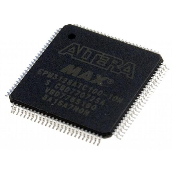
For system integrators, manufacturers, and maintenance teams, the value of the Break CPLD EPM3128ATC100-7 Software service is substantial. It enables continued operation of legacy systems, reduces the need for complete redesign, and preserves proven logic implementations that are difficult to reproduce from scratch. Instead of abandoning equipment due to locked or secured programmable devices, organizations can regain access to essential configuration data and embedded logic resources. By combining expertise in programmable logic devices with disciplined handling of protected and encrypted environments, this service provides a reliable and practical solution for recovering and reusing critical design assets across multiple industries.
Attack IC LPC2119FBD64 Firmware
Attack IC LPC2119FBD64 Firmware is a professional service designed for authorized users who need to regain access to embedded program assets when original documentation or development files are no longer available. The LPC2119FBD64, based on an ARM7TDMI-S core, has been widely adopted in industrial controllers, access control systems, automotive subsystems, energy management equipment, medical instruments, and communication devices. Its combination of performance, reliability, and flexible embedded peripherals makes it a long-standing choice in products that must remain operational for many years.
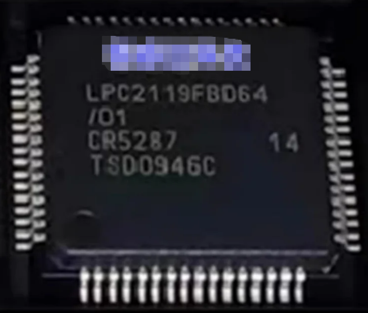
This microcontroller integrates on-chip flash memory, SRAM, multiple communication interfaces, and robust interrupt handling within a compact embedded architecture. To protect intellectual property, many deployments enable protective, protected, locked, or encrypted mechanisms that restrict access to firmware, binary, or heximal data stored in memory. While these measures are critical during production, they can limit maintenance, system upgrades, or controlled duplication later in the product lifecycle. Our Attack IC LPC2119FBD64 Firmware service focuses on helping clients attack and break such access barriers in a responsible engineering context, enabling retrieval of essential program archives without disclosing sensitive implementation details.
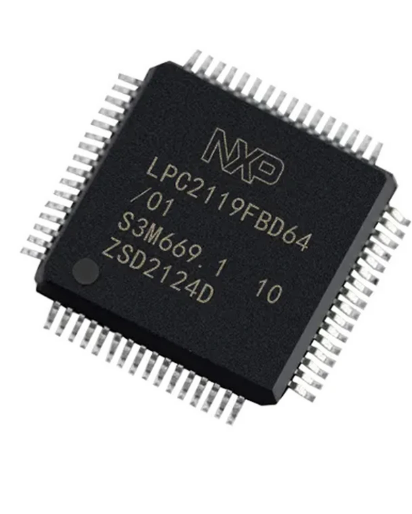
At a conceptual level, firmware recovery from a secured ARM-based controller requires an understanding of how flash, EEPROM-related data regions, and protection logic interact inside the device. Each case presents unique challenges, including secured boot processes, restricted debug interfaces, and verification logic designed to prevent unauthorized readout. Rather than relying on a single approach, the process emphasizes careful analysis, decoding of memory organization, and reconstruction of consistent firmware data. The objective is to retrieve usable program files—whether firmware, binary, or heximal—that can be validated, archived, and prepared for clone or duplicate purposes while preserving data integrity.
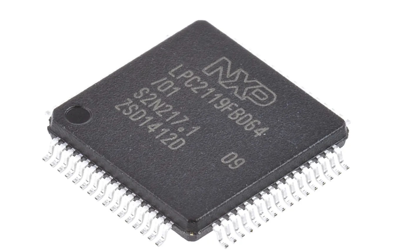
For end users, the value of this service is both technical and commercial. Access to recovered source code equivalents and program data allows legacy systems to be maintained, refurbished, or migrated to new platforms without a complete redesign. It reduces downtime, lowers redevelopment costs, and protects long-term investments in proven embedded solutions. By offering a discreet and disciplined solution for LPC2119FBD64 firmware retrieval, we support manufacturers, integrators, and service teams who depend on secured embedded devices and require reliable methods to retrieve critical memory data across a wide range of industries.
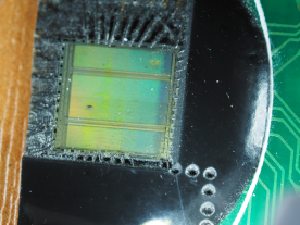
We can Attack IC LPC2119FBD64 Firmware, please view below IC LPC2119FBD64 features for your reference:
16/32-bit ARM7TDMI-S microcontroller in a tiny LQFP64 package.
16 kB on-chip Static RAM.
128/256 kB on-chip Flash Program Memory. 128-bit wide interface/accelerator enables high speed 60 MHz operation. In-System Programming (ISP) and In-Application Programming (IAP) via on-chip boot-loader software. Flash programming takes 1 ms per 512 byte line. Single sector or full chip erase takes 400 ms
EmbeddedICE-RT interface enables breakpoints and watch points. Interrupt service routines can continue to execute while the foreground task is debugged with the on-chip RealMonitor™ software.
Embedded Trace Macrocell enables non-intrusive high speed real-time tracing of instruction execution
Two interconnected CAN interfaces with advanced acceptance filters.
Four channel 10-bit A/D converter with conversion time as low as 2.44 µs.
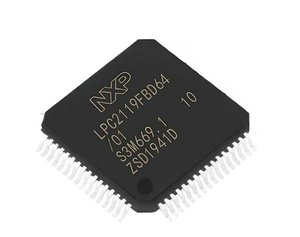
Multiple serial interfaces including two UARTs (16C550), Fast I2C (400 kbits/s) and two SPIs 60 MHz maximum CPU clock available from programmable on-chip
Phase-Locked Loop with settling time of 100 µs.
Vectored Interrupt Controller with configurable priorities and vector addresses.
Two 32-bit timers (with four capture and four compare channels), PWM unit (six outputs), Real Time Clock and Watchdog
Up to forty-six 5 V tolerant general purpose I/O pins. Up to nine edge or level sensitive external interrupt pins available.
On-chip crystal oscillator with an operating range of 1 MHz to 30 MHz
Two low power modes, Idle and Power-down.
Processor wake-up from Power-down mode via external interrupt.
Individual enable/disable of peripheral functions for power optimization.
Dual power supply:
CPU operating voltage range of 1.65 V to 1.95 V (1.8 V ±0.15 V).
I/O power supply range of 3.0 V to 3.6 V (3.3 V ± 10 %) with 5 V tolerant I/O pads.