Archive for the ‘Break IC’ Category
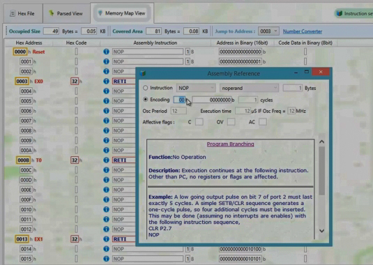
 Break MCU PIC10F200 Program
We can Break MCU PIC10F200 Program, below its the MCU PIC10F200 features for your reference:
Low-Power Features/CMOS Technology:
· Operating Current:
– < 175 ìA @ 2V, 4 MHz, typical
· Standby Current:
High-Performance RISC CPU:
· Only 33 single-word instructions to learn when Break MCU
· All single-cycle instructions except for program
branches, which are two-cycle
· 12-bit wide instructions
· 2-level deep hardware stack
· Direct, Indirect and Relative Addressing modes
for data and instructions
· 8-bit wide data path
· 8 Special Function Hardware registers
· Operating speed:
– 4 MHz internal clock
– 1 ìs instruction cycle if Break MCU
Special Microcontroller Features:
· 4 MHz precision internal oscillator:
– Factory calibrated to ±1%
· In-Circuit Serial Programming™ (ICSP™)
· In-Circuit Debugging (ICD) support
· Power-on Reset (POR)
· Device Reset Timer (DRT)
· Watchdog Timer (WDT) with dedicated on-chip after Break MCU
RC oscillator for reliable operation
· Programmable code protection
· Multiplexed MCLR input pin
· Internal weak pull-ups on I/O pins
· Power-Saving Sleep mode
· Wake-up from Sleep on pin change
– 100 nA @ 2V, typical
· Low-power, high-speed Flash technology:
– 100,000 Flash endurance
– > 40 year retention
· Fully static design
· Wide operating voltage range: 2.0V to 5.5V before Break MCU
· Wide temperature range:
– Industrial: -40°C to +85°C
– Extended: -40°C to +125°C
Peripheral Features (PIC10F200/202):
· 4 I/O pins:
– 3 I/O pins with individual direction control
– 1 input-only pin
– High current sink/source for direct LED drive before Break MCU
– Wake-on-change
– Weak pull-ups
· 8-bit real-time clock/counter (TMR0) with 8-bit programmable prescaler
Peripheral Features (PIC10F204/206):
· 4 I/O pins:
– 3 I/O pins with individual direction control
– 1 input-only pin
– High current sink/source for direct LED drive
– Wake-on-change
– Weak pull-ups
· 8-bit real-time clock/counter (TMR0) with 8-bit programmable prescaler when Break MCU
· 1 Comparator:
– Internal absolute voltage reference
– Both comparator inputs visible externally
– Comparator output visible externally
Decompiled firmware binary of secured system to C/C++ soure code
In today’s fast-paced tech world, many organizations face the challenge of working with firmware that has been intentionally obfuscated or secured to prevent reverse engineering. Whether for security audits, vulnerability assessments, or system optimization, understanding and modifying such firmware is a critical step in gaining full control of embedded systems. At Circuit Engineering CO.,LTD, we specialize in helping clients disassemble and reverse-engineer these complex, secured firmware binaries to provide clear, usable C/C++ source code.
At Circuit Engineering CO.,LTD, we specialize in helping clients disassemble and reverse-engineer these complex, secured firmware binaries to provide clear, usable C/C++ source code.
The Challenge of Obfuscated Firmware
Obfuscated firmware is designed to hide its underlying logic and make reverse engineering difficult. Many manufacturers intentionally encrypt, compress, or scramble the binary/heximal firmware to prevent competitors or malicious actors from accessing proprietary code or identifying vulnerabilities. The result is a binary that is hard to read, understand, or modify.
However, despite these challenges, disassembling obfuscated firmware is crucial for various applications, including bug fixing, custom modifications, security patching, and gaining deeper insight into the system’s functioning. This is where we come in.
firmware-ul obscurcat este conceput pentru a-și ascunde logica de bază și pentru a face dificilă ingineria inversă. Mulți producători criptează, comprimă sau amestecă în mod intenționat firmware-ul binar/heximal pentru a împiedica concurenții sau actorii rău intenționați să acceseze codul proprietar sau să identifice vulnerabilități. Rezultatul este un binar greu de citit, înțeles sau modificat.
Cu toate acestea, în ciuda acestor provocări, dezasamblarea firmware-ului obscurcat este crucială pentru diverse aplicații, inclusiv remedierea erorilor, modificările personalizate, corecțiile de securitate și obținerea unei cunoștințe mai profunde asupra funcționării sistemului. Aici intrăm noi.
Our Approach: Disassembling to Assembly Language and Decompiling to C/C++ Code
Our team of experts uses advanced techniques to disassemble the binary/heximal firmware into assembly language, the low-level programming code that the hardware executes directly. This is the foundational step in understanding how the firmware interacts with the hardware.
Once the firmware is in assembly language, we leverage powerful decompilation tools and custom scripts to reverse-engineer the assembly code into higher-level C/C++ source code. This source code is far more human-readable and modifiable, providing our clients with the ability to make necessary changes, improvements, or security patches.
Unser Expertenteam verwendet fortschrittliche Techniken, um die binäre/hexadezimale Firmware in Assemblersprache zu zerlegen, den Low-Level-Programmiercode, den die Hardware direkt ausführt. Dies ist der grundlegende Schritt zum Verständnis der Interaktion zwischen Firmware und Hardware.
Sobald die Firmware in Assemblersprache vorliegt, nutzen wir leistungsstarke Dekompilierungstools und benutzerdefinierte Skripte, um den Assemblercode in höherstufigen C/C++-Quellcode zurückzuentwickeln. Dieser Quellcode ist für Menschen weitaus besser lesbar und veränderbar und bietet unseren Kunden die Möglichkeit, notwendige Änderungen, Verbesserungen oder Sicherheitspatches vorzunehmen.
Why Choose Us?
-
Expertise in Reverse Engineering: Our team has years of experience in firmware disassembly and reverse engineering, particularly for secured and obfuscated firmware binaries.
-
Tailored Solutions: We understand that every client’s needs are different. Whether you need to extract specific data, debug software, or perform a detailed audit, we provide customized solutions.
-
Security and Confidentiality: We prioritize security and confidentiality in all our reverse engineering projects, ensuring that your intellectual property remains protected at all times.
-
Cutting-Edge Tools: We utilize the latest software tools and techniques to decompile and disassemble firmware efficiently and accurately.
facem posibilă deblocarea întregului potențial al firmware-ului securizat, ofuscat, dându-vă puterea de a îmbunătăți, audita sau modifica cu precizie sistemele dvs. încorporate. Prin conversia fișierelor binare complexe de firmware în cod sursă C/C++, vă oferim informațiile de care aveți nevoie pentru a prelua controlul asupra dispozitivelor dvs. încorporate.
Conclusion
At CECL, we make it possible to unlock the full potential of secured, obfuscated firmware, empowering you to enhance, audit, or modify your embedded systems with precision. By converting complex firmware binaries into C/C++ source code, we give you the insights you need to take control of your embedded devices.
If you’re facing the challenge of dealing with obfuscated firmware, reach out to us today, and let our experts help you navigate the complexities of reverse engineering.
Restoring Original Logic from Obfuscated Firmware: A Service You Can Rely On
In today’s fast-paced technological landscape, embedded systems and firmware are at the core of countless devices and machinery. However, when it comes to understanding and modifying firmware, the challenge often lies in the obfuscation techniques used to protect intellectual property or prevent unauthorized access. At Circuit Engineering CO.,LTD, we specialize in providing a robust service for compiled hexadecimal of embedded firmware to original logic restoration, enabling clients to reverse-engineer, analyze, and optimize embedded firmware.
However, when it comes to understanding and modifying firmware, the challenge often lies in the obfuscation techniques used to protect intellectual property or prevent unauthorized access. At Circuit Engineering CO.,LTD, we specialize in providing a robust service for compiled hexadecimal of embedded firmware to original logic restoration, enabling clients to reverse-engineer, analyze, and optimize embedded firmware
Understanding the Challenge
Obfuscation of binary or hexadecimal firmware is a common practice to protect proprietary code and prevent tampering or unauthorized modifications. This results in a compiled firmware that is hard to understand, with valuable logic often buried in complex, encrypted, or fragmented code. When clients encounter these challenges, they face difficulty in conducting vital tasks such as debugging, security assessments, or simply understanding the inner workings of a device.
Obfuzarea firmware-ului binar sau hexazecimal este o practică comună pentru a proteja codul proprietar și pentru a preveni manipularea sau modificările neautorizate. Acest lucru are ca rezultat un firmware compilat greu de înțeles, cu o logică valoroasă adesea îngropată în cod complex, criptat sau fragmentat. Când clienții se confruntă cu aceste provocări, se confruntă cu dificultăți în a efectua sarcini vitale, cum ar fi depanarea, evaluările de securitate sau pur și simplu înțelegerea funcționării interioare a unui dispozitiv.
Our service focuses on the process of disassembling obfuscated binary/hexadecimal firmware into assembly language, providing a deeper understanding of the firmware’s structure, logic, and functionality. By doing so, we restore the original logic of the embedded system, making it accessible and understandable for further analysis and improvement.
Unser Service konzentriert sich auf den Prozess der Zerlegung verschleierter binärer/hexadezimaler Firmware in Assemblersprache und ermöglicht so ein tieferes Verständnis der Struktur, Logik und Funktionalität der Firmware. Auf diese Weise stellen wir die ursprüngliche Logik des eingebetteten Systems wieder her und machen es für weitere Analysen und Verbesserungen zugänglich und verständlich.
How We Help
Our team of experienced engineers employs cutting-edge reverse engineering techniques to meticulously disassemble the compiled firmware. The process involves several key steps:
Firmware Analysis: We begin by analyzing the compiled hexadecimal or binary file to identify the obfuscation techniques applied, including encryption, packing, and fragmentation.
Deobfuscation and Decompression: Using specialized tools and proprietary methods, we deobfuscate and decompress the firmware to reveal its underlying structure.
Disassembly to Assembly: After successfully deobfuscating the binary, we disassemble it into assembly language, which is easier to interpret and modify.
Logic Restoration: Finally, we restore the original logic, functions, and routines, allowing you to understand the exact behavior of the embedded system.
Analiza firmware: Începem prin a analiza fișierul hexazecimal sau binar compilat pentru a identifica tehnicile de ofuscare aplicate, inclusiv criptarea, împachetarea și fragmentarea.
Deofuscare și decompresie: Folosind instrumente specializate și metode proprietare, deobfucăm și decomprimăm firmware-ul pentru a dezvălui structura de bază.
Dezasamblare la asamblare: după dezfundarea cu succes a binarului, îl dezasamblam în limbaj de asamblare, care este mai ușor de interpretat și modificat.
Restaurare logică: În cele din urmă, restaurăm logica, funcțiile și rutinele originale, permițându-vă să înțelegeți comportamentul exact al sistemului încorporat.
Why Choose Us?
We are committed to delivering high-quality, efficient, and precise firmware restoration services. Our expertise ensures that no matter how obfuscated or encrypted the firmware is, we can help restore it to its original logic, enabling better analysis, optimization, and security. Whether you are a hardware manufacturer, a security researcher, or an enterprise needing to update or modify embedded firmware, we provide reliable solutions tailored to your specific needs.
Let us assist you in turning complex, obfuscated firmware into valuable, understandable assembly code for your next project.
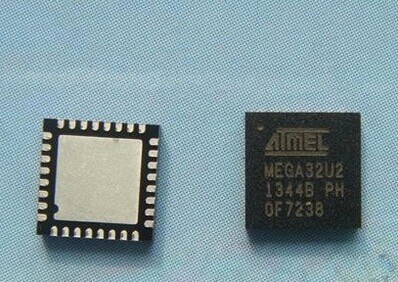
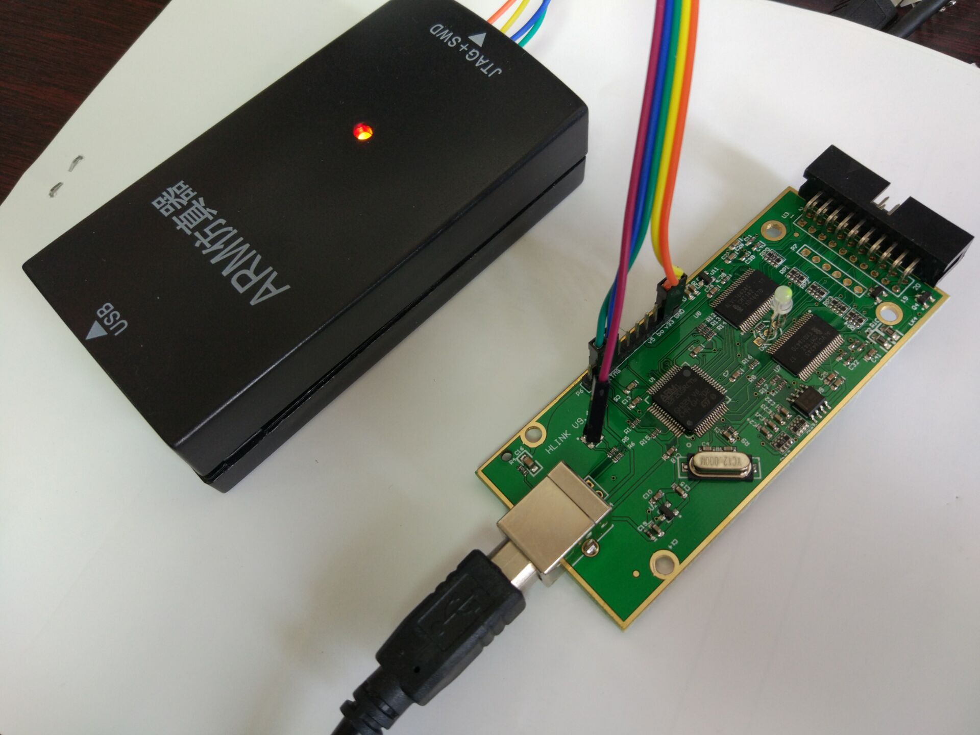
Break Locked ATmega32U2 Microprocessor Flash
Break Locked ATmega32U2 Microprocessor Flash and copy heximal firmware to new atmega32u2 flash memory and eeprom memory, the source code of binary program and data will be pull out from original master mcu atmega32u2;
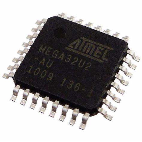
Break Locked ATmega32U2 Microprocessor Flash and copy heximal firmware to new atmega32u2 flash memory and eeprom memory, the source code of binary program and data will be pull out from original master mcu atmega32u2
Input to the inverting Oscillator amplifier and input to the internal clock operating circuit. Output from the inverting Oscillator amplifier if enabled by Fuse. Also serves as a generic I/O. This documentation contains simple code examples that briefly show how to use various parts of the device. Be aware that not all C compiler vendors include bit definitions in the header files and interrupt handling in C is compiler dependent. Please confirm with the C compiler documen- tation for more details.
These code examples assume that the part specific header file is included before compilation. For I/O registers located in extended I/O map, “IN”, “OUT”, “SBIS”, “SBIC”, “CBI”, and “SBI” instructions must be replaced with instructions that allow access to extended I/O. Typically “LDS” and “STS” combined with “SBRS”, “SBRC”, “SBR”, and “CBR”. Reliability Qualification results show that the projected data retention failure rate is much less than 1 PPM over 20 years at 85°C or 100 years at 25°C.
reverse engineering ATMEGA32U2 secured mcu fuse bit and dump firmware binary or heximal out of ATMEGA32U2 flas memory
This section discusses the AVR core architecture in general. The main function of the CPU core is to ensure correct program execution. The CPU must therefore be able to access memories when reversing atmega16u2 microcontroller protection, perform calculations, control peripherals, and handle interrupts.
Break Locked ATmega32U2 Microprocesador Flash y copie el firmware heximal a la nueva memoria flash atmega32u2 y memoria eeprom, el código fuente del programa binario y los datos se extraerán del mcu maestro original atmega32u2
In order to maximize performance and parallelism, the AVR uses a Harvard architecture – with separate memories and buses for program and data. Instructions in the program memory are executed with a single level pipelining. While one instruction is being executed, the next instruction is prefetched from the program memory after recovering atmega8u2 encrypted microprocessor flash memory. This concept enables instructions to be executed in every clock cycle. The program memory is In-System Reprogrammable Flash memory.
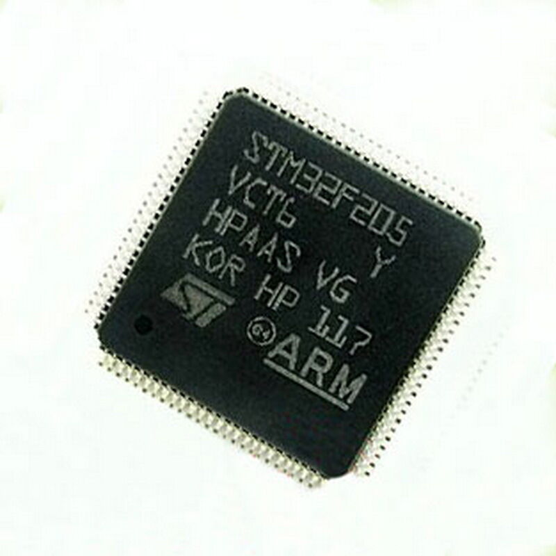
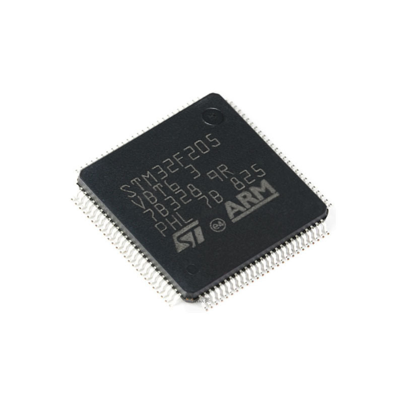
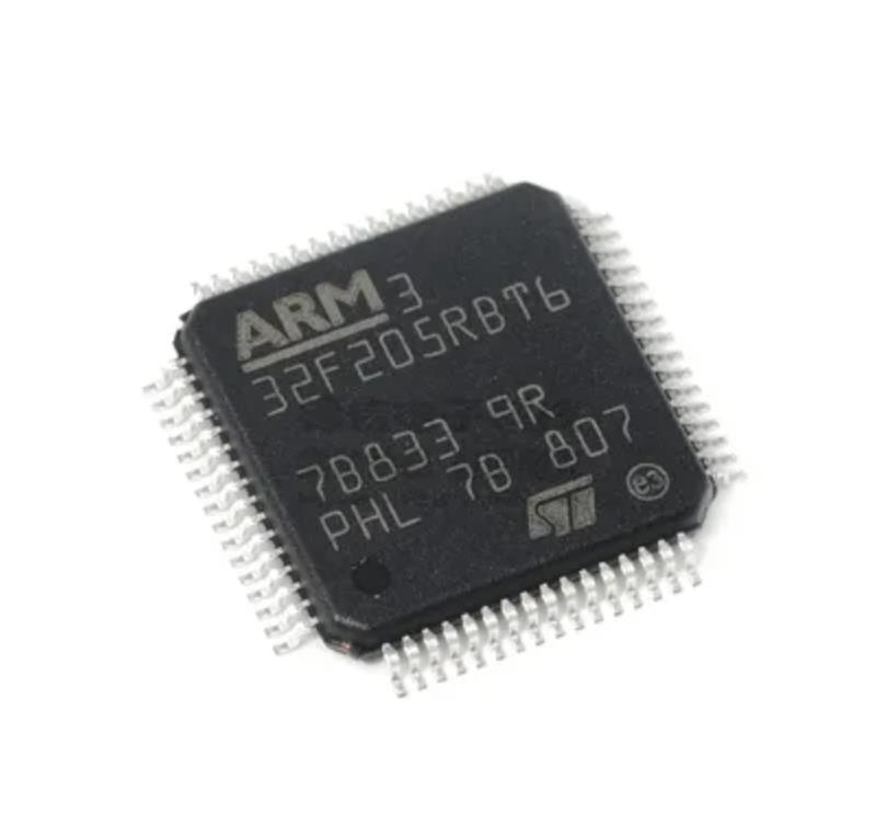
Break STM32F205VCT6 MCU Chip Flash Memory
Break STM32F205VCT6 MCU Chip Flash Memory needs to crack stm32f205vct6 arm mcu protective system, copy embedded flash program to new microcontroller stm32f205vct6;
Break STM32F205VCT6 MCU Chip Flash Memory needs to crack stm32f205vct6 arm mcu protective system, copy embedded flash program to new microcontroller stm32f205vct6
The two DMA controllers support circular buffer management, so that no specific code is needed when the controller reaches the end of the buffer. The two DMA controllers also have a double buffering feature, which automates the use and switching of two memory buffers without requiring any special code when breaking stm32f205rbt6 mcu flash memory protection.
romper STM32F205VCT6 La memoria flash del chip MCU necesita descifrar stm32f205vct6 armar el sistema de protección mcu, copiar el programa flash integrado al nuevo microcontrolador stm32f205vct6
Each stream is connected to dedicated hardware DMA requests, with support for software trigger on each stream. Configuration is made by software and transfer sizes between source and destination are independent.
The FSMC is embedded in all STM32F20x devices. It has four Chip Select outputs supporting the following modes: PC Card/Compact Flash, SRAM, PSRAM, NOR Flash and NAND Flash.
attack protective arm mcu stm32f205vct6 flash memory and clone its heximal content
Functionality overview:
- Write FIFO
- Code execution from external memory except for NAND Flash and PC Card
- Maximum frequency (fHCLK) for external access is 60 MHz
LCD parallel interface
The FSMC can be configured to interface seamlessly with most graphic LCD controllers. It supports the Intel 8080 and Motorola 6800 modes, and is flexible enough to adapt to specific LCD interfaces by recover stm32f205rct6 mcu flash memory program. This LCD parallel interface capability makes it easy to build cost- effective graphic applications using LCD modules with embedded controllers or high performance solutions using external controllers with dedicated acceleration.
Attack STMicroelectronics STM32F205VB MCU Protection
Attack STMicroelectronics STM32F205VB MCU Protection and unlock stm32f205vbt6 secured microcontroller flash program file after copy flash heximal file to stm32f205vb arm chip;
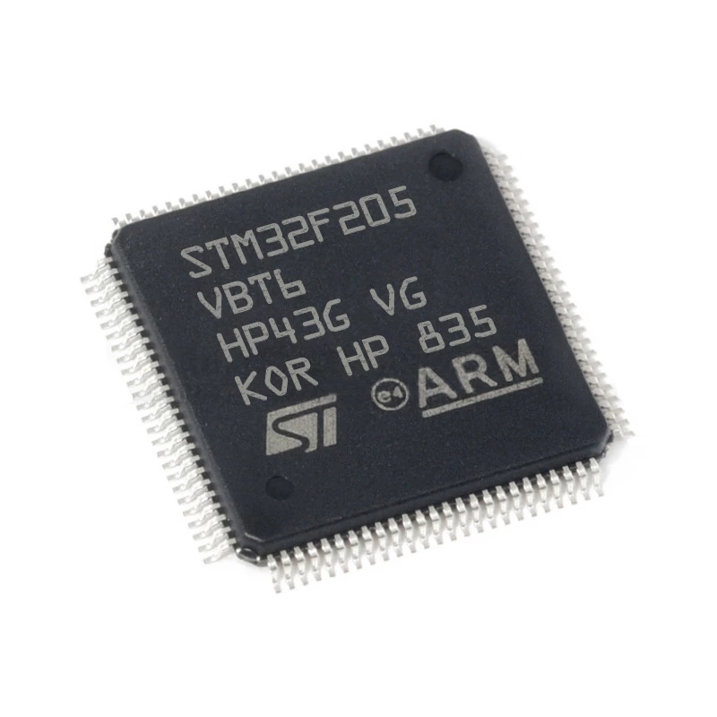
Attack STMicroelectronics STM32F205VB MCU Protection and unlock stm32f205vbt6 secured microcontroller flash program file after copy flash heximal file to stm32f205vb arm chip
The CRC (cyclic redundancy check) calculation unit is used to get a CRC code from a 32-bit data word and a fixed generator polynomial.
Among other applications, CRC-based techniques are used to verify data transmission or storage integrity. In the scope of the EN/IEC 60335-1 standard by breaking arm mcu chip stm32f205rb flash memory, they offer a means of verifying the Flash memory integrity. The CRC calculation unit helps compute a software signature during runtime, to be compared with a reference signature generated at link-time and stored at a given memory location.
ataque STMicroelectronics STM32F205VB MCU protección y desbloqueo stm32f205vbt6 archivo de programa flash del microcontrolador seguro después de copiar el archivo flash heximal al chip arm stm32f205vb
All STM32F20x products embed:
- Up to 128 Kbytes of system SRAM accessed (read/write) at CPU clock speed with 0 wait states
- 4 Kbytes of backup
The content of this area is protected against possible unwanted write accesses, and is retained in Standby or VBAT mode.
The 32-bit multi-AHB bus matrix interconnects all the masters (CPU, DMAs, Ethernet, USB HS) and the slaves (Flash memory, RAM, FSMC, AHB and APB peripherals) and ensures a seamless and efficient operation even when several high-speed peripherals work simultaneously.
hack stm32f205vbt6 microcontroller fuse bit and dump binary out from flash memory
The devices feature two general-purpose dual-port DMAs (DMA1 and DMA2) with 8 streams each. They are able to manage memory-to-memory, peripheral-to-memory and memory-to-peripheral transfers. They share some centralized FIFOs for APB/AHB peripherals, support burst transfer and are designed to provide the maximum peripheral bandwidth (AHB/APB).
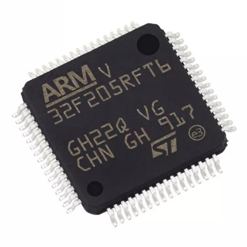
Attack ARM STM32F205RF Microprocessor Tamper Resistance
Attack ARM STM32F205RF Microprocessor Tamper Resistance and decode stm32f205rf secured memory software from its flash, then read out microcontroller stm32f205rf flash memory content;
Attack ARM STM32F205RF Microprocessor Tamper Resistance and decode stm32f205rf secured memory software from its flash, then read out microcontroller stm32f205rf flash memory content;
The Arm® Cortex®-M3 processor is the latest generation of processors for embedded systems. It was developed to provide a low-cost platform that meets the needs of MCU implementation, with a reduced pin count and low-power consumption by recovering stm32f205rc microcontroller flash heximal, while delivering outstanding computational performance and an advanced response to interrupts.
The Arm® Cortex®-M3 32-bit RISC processor features exceptional code-efficiency, delivering the high-performance expected from an Arm core in the memory size usually associated with 8- and 16-bit devices. With its embedded Arm® core, the STM32F20x family is compatible with all Arm® tools and software.
Ataque la resistencia a la manipulación del microprocesador ARM STM32F205RF y decodifique el software de memoria protegida stm32f205rf desde su flash, luego lea el contenido de la memoria flash del microcontrolador stm32f205rf
The ART Accelerator™ is a memory accelerator which is optimized for STM32 industry- standard Arm® Cortex®-M3 processors. It balances the inherent performance advantage of the Arm® Cortex®-M3 over Flash memory technologies to break off stm32f205rb mcu flash memory, which normally requires the processor to wait for the Flash memory at higher operating frequencies.
unlock protected STM32F205RFT6 microprocessor fuse bit and readout embedded firmware from mcu chip STM32F205RFT6 flash memory
To release the processor full 150 DMIPS performance at this frequency, the accelerator implements an instruction prefetch queue and branch cache which increases program execution speed from the 128-bit Flash memory. Based on CoreMark® benchmark, the performance achieved thanks to the ART accelerator is equivalent to 0 wait state program execution from Flash memory at a CPU frequency up to 120 MHz.
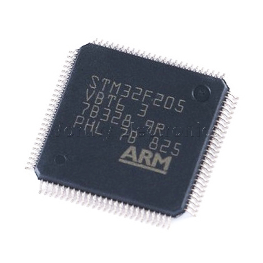
Break ARM STM32F205RB MCU Flash Memory
Break ARM STM32F205RB MCU Flash Memory and read embedded firmware out from STM32F205RB microcontroller, copy arm cortex3 stm32f205rb program binary to new microprocessor;
Break ARM STM32F205RB MCU Flash Memory and read embedded firmware out from STM32F205RB microcontroller, copy arm cortex3 stm32f205rb program binary to new microprocessor
The STM32F20x family is based on the high-performance Arm® Cortex®-M3 32-bit RISC core operating at a frequency of up to 120 MHz to recover microcontroller stm32f105rc flash memory content. The family incorporates high-speed embedded memories (Flash memory up to 1 Mbyte, up to 128 Kbytes of system SRAM), up to 4 Kbytes of backup SRAM, and an extensive range of enhanced I/Os and peripherals connected to two APB buses, three AHB buses and a 32-bit multi-AHB bus matrix.
The devices also feature an adaptive real-time memory accelerator (ART Accelerator™) that allows to achieve a performance equivalent to 0 wait state program execution from Flash memory at a CPU frequency up to 120 MHz. This performance has been validated using the CoreMark® benchmark.
разблокировать защищенный предохранитель микропроцессора stm32f205rbt6 и скопировать шестнадцатеричную программу прошивки из флэш-памяти микрокомпьютера stm32f205rbt6
All devices offer three 12-bit ADCs, two DACs, a low-power RTC, twelve general-purpose 16-bit timers including two PWM timers for motor control, two general-purpose 32-bit timers. a true number random generator (RNG). They also feature standard and advanced communication interfaces when breaking off stm32f101c4 flash memory firmware. New advanced peripherals include an SDIO, an enhanced flexible static memory control (FSMC) interface (for devices offered in packages of 100 pins and more), and a camera interface for CMOS sensors. The devices also feature standard peripherals.
- Up to three I2Cs
- Three SPIs, two I2 To achieve audio class accuracy, the I2S peripherals can be clocked via a dedicated internal audio PLL or via an external PLL to allow synchronization.
- Four USARTs and two UARTs
- A USB OTG high-speed with full-speed capability (with the ULPI)
- A second USB OTG (full-speed)
- Two CANs
- An SDIO interface
- Ethernet and camera interface available on STM32F207xx devices
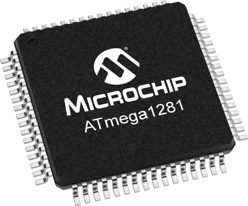
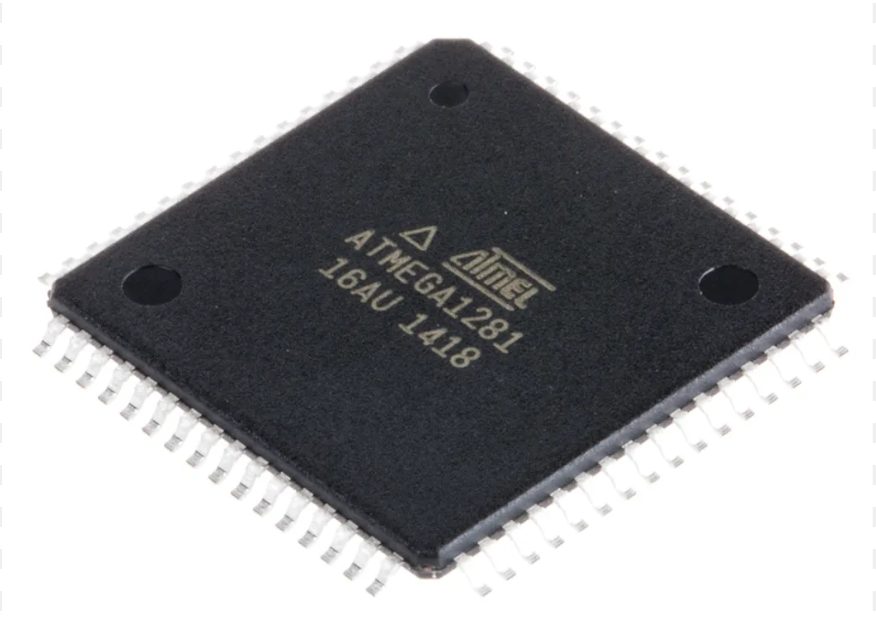
Locked Microcontroller ATmega1281 Flash Memory Breaking
Locked Microcontroller ATmega1281 Flash Memory Breaking is a process to unlock microprocessor atmega1281 flash fuse bit and release software program from its memory and then copy firmware heximal to new mcu atmega1281 avr chip;
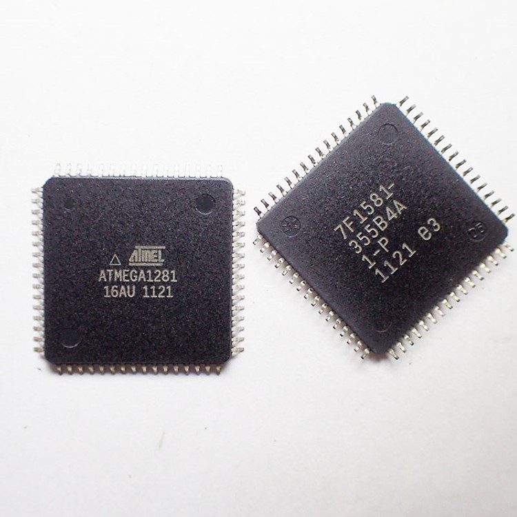
Locked Microcontroller ATmega1281 Flash Memory Breaking is a process to unlock microprocessor atmega1281 flash fuse bit and release software program from its memory and then copy firmware heximal to new mcu atmega1281 avr chip;
This section discusses the AVR core architecture in general. The main function of the CPU core is to ensure cor- rect program execution. The CPU must therefore be able to access memories, perform calculations, control peripherals, and handle interrupts.
In order to maximize performance and parallelism, the AVR uses a Harvard architecture – with separate memories and buses for program and data. Instructions in the program memory are executed with a single level pipelining by reverse engineering microcontroller atmega1281 program. While one instruction is being executed, the next instruction is pre-fetched from the program memory. This concept enables instructions to be executed in every clock cycle. The program memory is In-System Reprogrammable Flash memory.
crack atmega1281 mcu flash protective system and extract embedded binary file from flash memory
The fast-access Register File contains 32 × 8-bit general purpose working registers with a single clock cycle access time. This allows single-cycle Arithmetic Logic Unit (ALU) operation. In a typical ALU operation, two operands are output from the Register File, the operation is executed, and the result is stored back in the Register File– in one clock cycle by reverse engineering atmega1281 mcu firmware.
Desbloquee los datos del programa del controlador Microchip ATMEGA1280V y lea la memoria flash mcu atmega1280v heximal, el contenido flash original del microcontrolador avr atmega1280v se decodificará
Six of the 32 registers can be used as three 16-bit indirect address register pointers for Data Space addressing – enabling efficient address calculations. One of the these address pointers can also be used as an address pointer for look up tables in Flash program memory. These added function registers are the 16-bit X-, Y-, and Z-register, described later in this section.
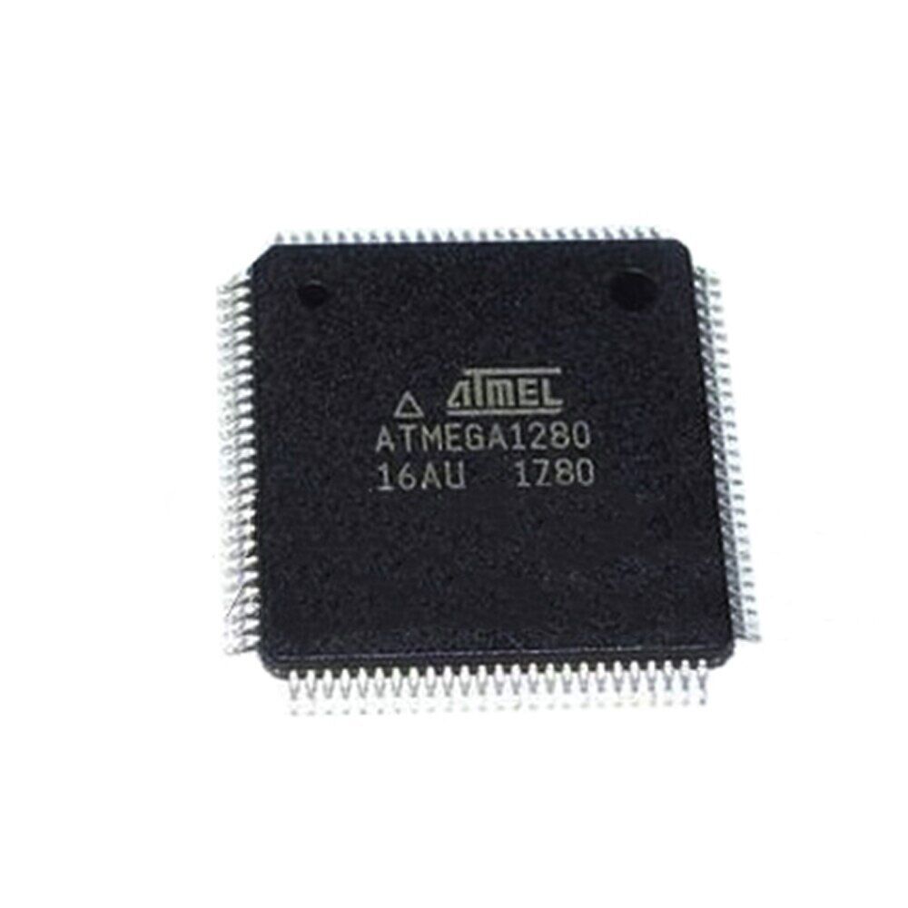
Unlock Microchip ATMEGA1280V Controller Program Data
Unlock Microchip ATMEGA1280V Controller Program Data and read mcu atmega1280v flash memory heximal, original avr microcontroller atmega1280v flash content will be decoding;
Unlock Microchip ATMEGA1280V Controller Program Data and read mcu atmega1280v flash memory heximal, original avr microcontroller atmega1280v flash content will be decoding
Port G is a 6-bit bi-directional I/O port with internal pull-up resistors (selected for each bit). The Port G output buffers have symmetrical drive characteristics with both high sink and source capability. As inputs, Port G pins that are externally pulled low will source current if the pull-up resistors are activated when breaking ic chip atmega1280v flash binary. The Port G pins are tri-stated when a reset condition becomes active, even if the clock is not running. Port G also serves the functions of various special features of the Atmel ATmega1280v as listed on page 72.
Desbloquee los datos del programa del controlador Microchip ATMEGA1280V y lea la memoria flash mcu atmega1280v heximal, el contenido flash original del microcontrolador avr atmega1280v se decodificará
Port H is a 8-bit bi-directional I/O port with internal pull-up resistors (selected for each bit). The Port H output buffers have symmetrical drive characteristics with both high sink and source capability. As inputs, Port H pins that are externally pulled low will source current if the pull-up resistors are activated. The Port H pins are tri-stated when a reset condition becomes active when recover microprocessor atmega1280v flash memory file, even if the clock is not running. Port H also serves the functions of various special features of the ATmega3250/6450 as listed on page 72.
clone atmega1280v microprocessor flash heximal and copy firmware code to new atmega1280v microcontroller and encrypt the chip
Port J is a 7-bit bi-directional I/O port with internal pull-up resistors (selected for each bit). The Port J output buffers have symmetrical drive characteristics with both high sink and source capa- bility. As inputs, Port J pins that are externally pulled low will source current if the pull-up resistors are activated. The Port J pins are tri-stated when a reset condition becomes active, even if the clock is not running.