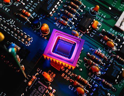
Archive for the ‘Reverse Engineer Microcontroller’ Category
 Breaking Down Compiled Binary to Human-Readable Assembly Code: Unlocking the Power of Embedded Systems
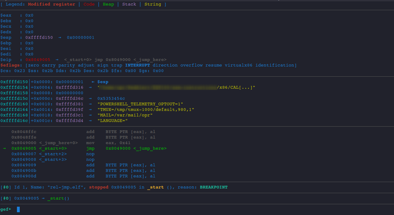
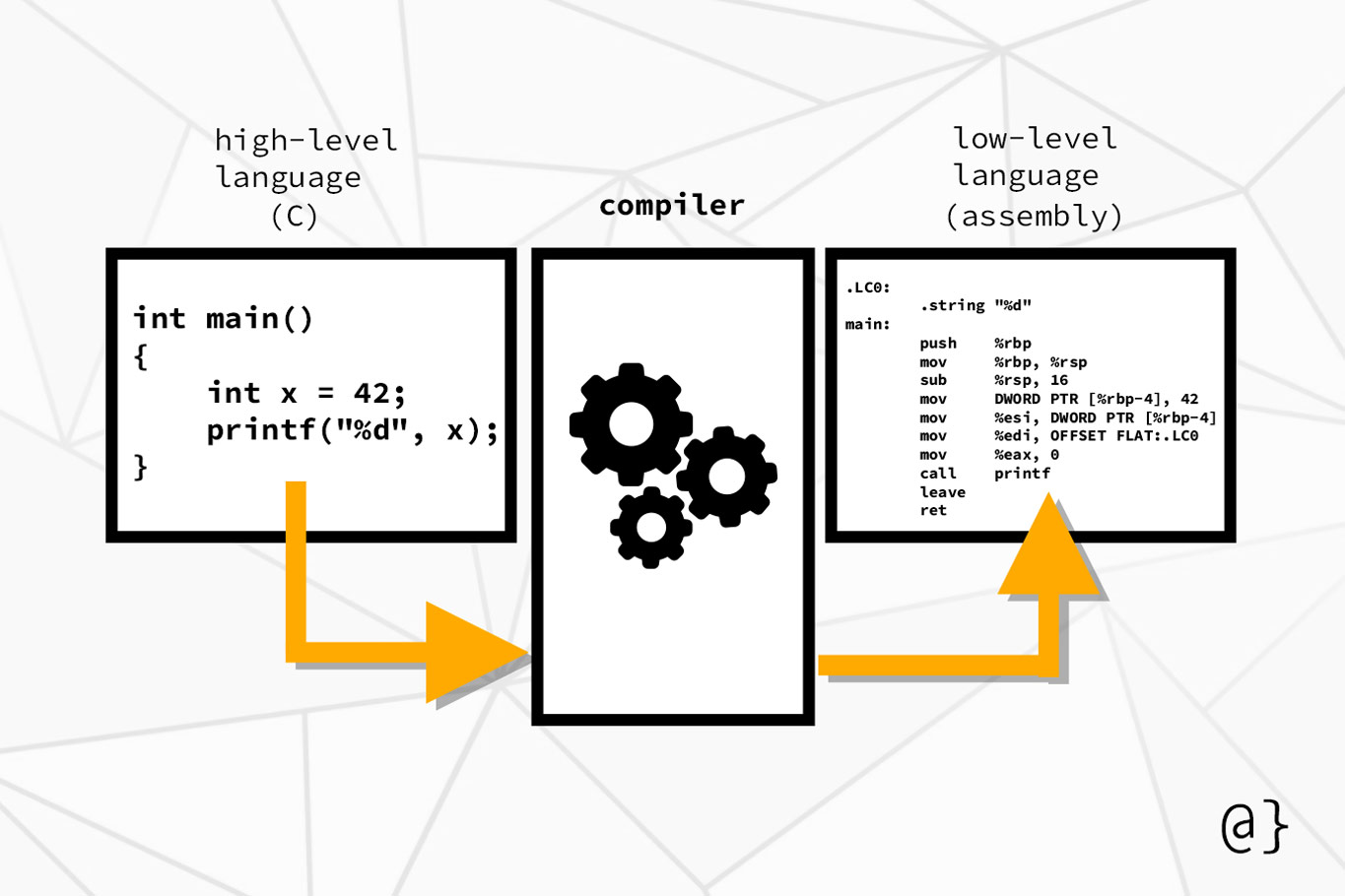
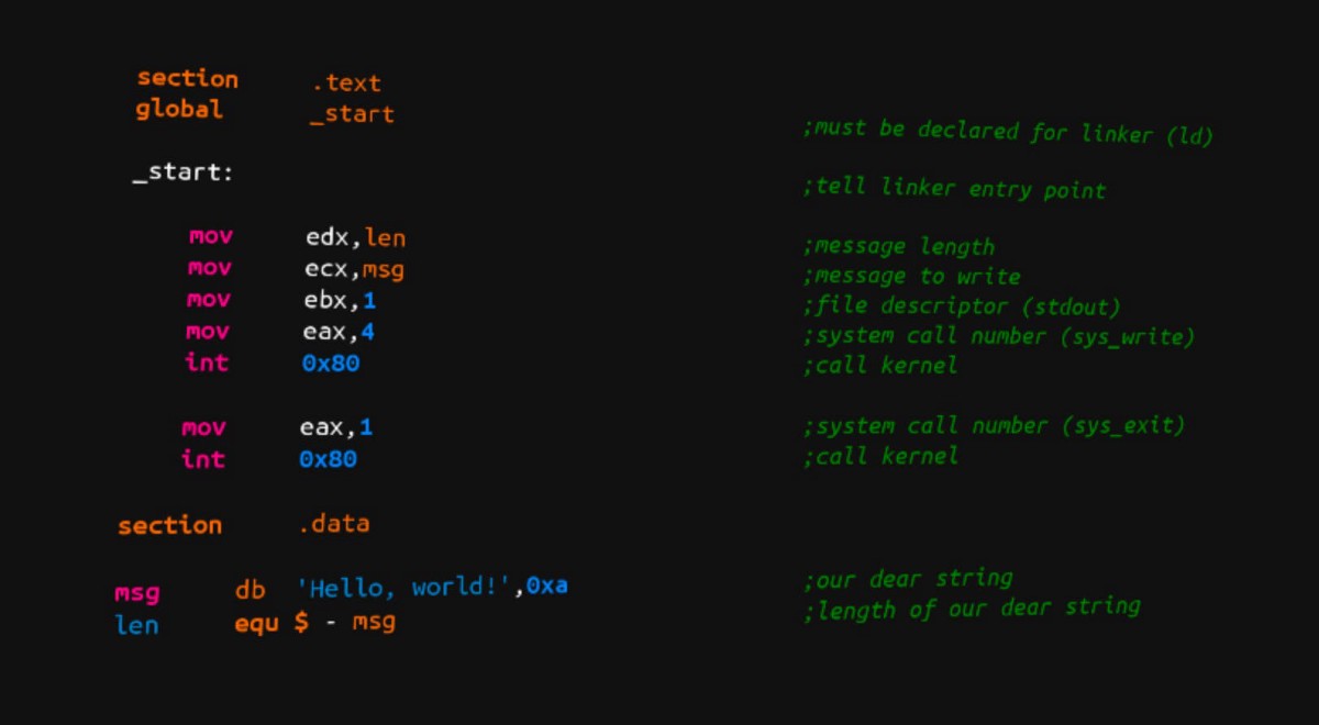
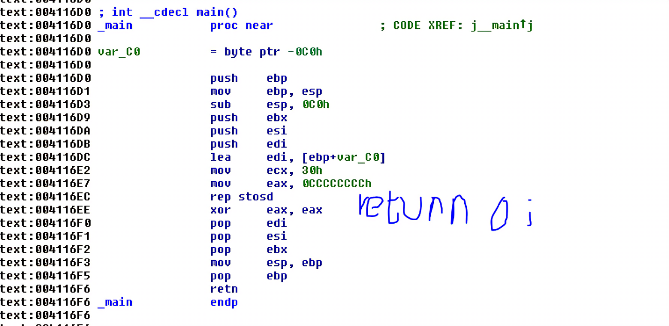
In the world of embedded systems, firmware is the backbone of functionality, often stored as compiled binary or hexadecimal files. However, when the original source code is lost, inaccessible, or simply unavailable, understanding and modifying the firmware becomes a significant challenge. This is where our specialized service, Breaking Down Compiled Binary to Human-Readable Assembly Code, comes into play.
Notre service est conçu pour transformer des binaires complexes compilés au niveau de la machine en code assembleur clair et lisible par l’homme. À l’aide d’outils et de techniques de désassemblage avancés, nous analysons méticuleusement le micrologiciel, révélant sa logique et sa structure sous-jacentes. Que vous travailliez avec un système hérité, que vous déboguiez un problème ou que vous amélioriez la compatibilité avec du matériel moderne, notre service vous fournit les informations dont vous avez besoin pour aller de l’avant.
Our service is designed to transform complex, machine-level compiled binaries into clear, human-readable assembly code. Using advanced disassembly tools and techniques, we meticulously analyze the firmware, revealing its underlying logic and structure. Whether you’re working with a legacy system, debugging an issue, or improving compatibility with modern hardware, our service provides the insights you need to move forward.
Our service is designed to transform complex, machine-level compiled binaries into clear, human-readable assembly code. Using advanced disassembly tools and techniques, we meticulously analyze the firmware, revealing its underlying logic and structure. Whether you’re working with a legacy system, debugging an issue, or improving compatibility with modern hardware, our service provides the insights you need to move forward.
Why Choose Our Service?
- Comprehensive Analysis: We delve deep into the compiled binary or hexadecimal files, extracting every detail to reconstruct the assembly code. This allows for a thorough understanding of the firmware’s behavior and functionality.
- Debugging Made Easy: By converting the compiled binary into assembly code, we enable precise debugging. You can trace execution paths, identify errors, and optimize performance with ease.
- Compatibility Improvements: Upgrading or integrating legacy systems with new hardware often requires firmware modifications. Our service provides the foundation for making these improvements seamlessly.
- Intellectual Property Recovery: Lost or inaccessible source code can halt development. We help recover critical information from compiled binaries, ensuring your projects stay on track.
종합 분석: 컴파일된 바이너리 또는 16진수 파일을 깊이 파고들어 모든 세부 사항을 추출하여 어셈블리 코드를 재구성합니다. 이를 통해 펌웨어의 동작과 기능을 철저히 이해할 수 있습니다.
디버깅을 쉽게: 컴파일된 바이너리를 어셈블리 코드로 변환하여 정확한 디버깅을 가능하게 합니다. 실행 경로를 추적하고 오류를 식별하며 성능을 쉽게 최적화할 수 있습니다.
호환성 개선: 레거시 시스템을 새 하드웨어로 업그레이드하거나 통합하려면 종종 펌웨어 수정이 필요합니다. 당사 서비스는 이러한 개선을 원활하게 수행할 수 있는 기반을 제공합니다.
지적 재산 복구: 소스 코드가 손실되거나 액세스할 수 없으면 개발이 중단될 수 있습니다. 당사는 컴파일된 바이너리에서 중요한 정보를 복구하여 프로젝트가 제대로 진행되도록 돕습니다.
Applications of Our Service
- Embedded System Development: Gain insights into firmware behavior for better design and optimization.
- Legacy System Upgrades: Modify and adapt old firmware for new hardware requirements.
- Security Audits: Analyze firmware for vulnerabilities or malicious code.
- Competitive Analysis: Understand competitor products by reverse engineering their firmware.
How We Work
Using state-of-the-art disassembly tools, we break down the compiled binary into assembly code. Our team of experts then analyzes the code, providing you with detailed documentation and actionable insights.
अत्याधुनिक डिसअसेंबली टूल का उपयोग करके, हम संकलित बाइनरी को असेंबली कोड में तोड़ते हैं। फिर हमारे विशेषज्ञों की टीम कोड का विश्लेषण करती है, और आपको विस्तृत दस्तावेज़ और कार्रवाई योग्य जानकारी प्रदान करती है।
चाहे आप डिबगिंग कर रहे हों, संगतता में सुधार कर रहे हों, या खोई हुई बौद्धिक संपदा को पुनः प्राप्त कर रहे हों, हमारी संकलित बाइनरी को मानव-पठनीय असेंबली कोड में तोड़ना सेवा एम्बेडेड सिस्टम की पूरी क्षमता को अनलॉक करने का आपका प्रवेश द्वार है। आइए हम जटिल मशीन कोड को स्पष्ट, कार्रवाई योग्य ज्ञान में बदलने में आपकी सहायता करें।
Whether you’re debugging, improving compatibility, or recovering lost intellectual property, our Breaking Down Compiled Binary to Human-Readable Assembly Code service is your gateway to unlocking the full potential of embedded systems. Let us help you turn complex machine code into clear, actionable knowledge.
Unlock the Potential of Your Embedded Systems with Our Microcontroller Firmware Reverse Engineering Service
In today’s fast-paced technological landscape, embedded systems are at the heart of countless devices, from industrial machinery to consumer electronics. However, many businesses face challenges when working with legacy systems, lost source code, or incompatible firmware. Our Microcontroller Firmware Reverse Engineering Service is designed to help you overcome these obstacles, providing you with the tools and insights needed to optimize, debug, and enhance your embedded systems.
embedded systems are at the heart of countless devices, from industrial machinery to consumer electronics. However, many businesses face challenges when working with legacy systems, lost source code, or incompatible firmware. Our Microcontroller Firmware Reverse Engineering Service is designed to help you overcome these obstacles, providing you with the tools and insights needed to optimize, debug, and enhance your embedded systems.
What is Microcontroller Firmware Reverse Engineering?
Reverse engineering is the process of analyzing a compiled binary or compiled hexadecimal file to reconstruct its original logic and functionality. Using advanced tools and techniques, we disassemble the firmware into assembly code or higher-level representations, allowing us to understand its structure, algorithms, and behavior. This process is invaluable for debugging, compatibility improvement, and recovering lost intellectual property.
L’ingénierie inverse est le processus d’analyse d’un fichier binaire compilé ou d’un fichier hexadécimal compilé pour reconstruire sa logique et ses fonctionnalités d’origine. À l’aide d’outils et de techniques avancés, nous désassemblons le micrologiciel en code assembleur ou en représentations de niveau supérieur, ce qui nous permet de comprendre sa structure, ses algorithmes et son comportement. Ce processus est inestimable pour le débogage, l’amélioration de la compatibilité et la récupération de la propriété intellectuelle perdue.
Our Expertise and Services
Our team of experts specializes in reverse engineering firmware for a wide range of microcontrollers and embedded systems. Whether you’re dealing with a legacy system, a corrupted firmware archive, or a secured MCU, we can help. Our services include:
- Firmware Analysis: Detailed examination of the compiled binary to identify functionality, vulnerabilities, or inefficiencies.
- Debugging and Troubleshooting: Pinpointing errors or bugs in the firmware to improve performance and reliability.
- Compatibility Improvement: Adapting firmware to work with new hardware or updated systems.
- Source Code Recovery: Reconstructing lost or inaccessible source code from compiled binaries.
- Firmware Extraction and Dumping: Retrieving firmware directly from the microcontroller’s memory for analysis or replication.
펌웨어 분석: 컴파일된 바이너리를 자세히 조사하여 기능, 취약성 또는 비효율성을 식별합니다.
디버깅 및 문제 해결: 성능과 안정성을 개선하기 위해 펌웨어의 오류 또는 버그를 정확히 파악합니다.
호환성 개선: 새로운 하드웨어 또는 업데이트된 시스템에서 작동하도록 펌웨어를 조정합니다.
소스 코드 복구: 컴파일된 바이너리에서 손실되거나 액세스할 수 없는 소스 코드를 재구성합니다.
펌웨어 추출 및 덤핑: 분석 또는 복제를 위해 마이크로컨트롤러의 메모리에서 직접 펌웨어를 검색합니다.
Why Choose Us?
With years of industry experience to deliver accurate and reliable results. Our non-invasive methods ensure that your hardware remains intact while we extract and analyze the firmware. Whether you’re looking to debug a problematic system, improve compatibility, or recover lost data, our Microcontroller Firmware Reverse Engineering Service provides the solutions you need.
सटीक और विश्वसनीय परिणाम देने के लिए उद्योग के वर्षों के अनुभव के साथ। हमारे गैर-आक्रामक तरीके यह सुनिश्चित करते हैं कि फ़र्मवेयर को निकालने और उसका विश्लेषण करने के दौरान आपका हार्डवेयर बरकरार रहे। चाहे आप किसी समस्याग्रस्त सिस्टम को डीबग करना चाहते हों, संगतता में सुधार करना चाहते हों या खोए हुए डेटा को पुनर्प्राप्त करना चाहते हों, हमारी माइक्रोकंट्रोलर फ़र्मवेयर रिवर्स इंजीनियरिंग सेवा आपको आवश्यक समाधान प्रदान करती है।
Unlock the full potential of your embedded systems today. Contact us to learn more about how we can help you achieve your goals with precision and expertise.
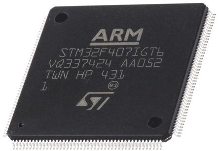
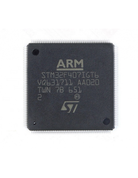
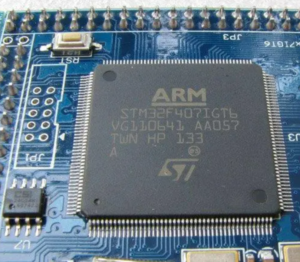
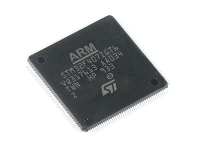
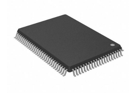
Reverse engineering MCU microchip STM32F407IG flash memory
Reverse engineering MCU microchip STM32F407IG flash memory to attack tamper resistance system of STM32F407IG microcontroller encryption and its fuse bit, extract program file from STM32F407IG microprocessor’s flash memory and dump source code in the format of binary file or heximal data to new STM32F407IG microcomputer;
The STM32F407IG microcontroller can be used in a wide range of products and applications across various industries due to its powerful features and versatility. Here are some examples of products and industries where the STM32F407IG can be employed:
Industrial Automation: The STM32F407IG can be used in industrial control systems, PLCs (Programmable Logic Controllers), motor control applications, and process automation systems. Its rich set of peripherals, including ADCs, DACs, timers, and communication interfaces, make it suitable for controlling and monitoring industrial processes.
Consumer Electronics: The STM32F407IG can be found in various consumer electronics products such as smart home devices, home appliances, audio systems, gaming peripherals, and wearable devices. Its low-power features, USB connectivity, and advanced processing capabilities make it ideal for such applications.
Medical Devices: In the medical industry, the STM32F407IG can be used in devices such as patient monitoring systems, infusion pumps, medical imaging equipment, and portable diagnostic devices. Its real-time processing capabilities, high-resolution ADCs, and communication interfaces enable the development of advanced medical devices.
Automotive: The STM32F407IG can be employed in automotive applications including engine control units (ECUs), dashboard systems, infotainment systems, and advanced driver assistance systems (ADAS). Its CAN interfaces, high-speed processing, and robust design make it suitable for automotive electronics.
Internet of Things (IoT): The STM32F407IG can be used in IoT devices and edge computing applications where connectivity, processing power, and low-power operation are essential. It can be found in smart sensors, IoT gateways, industrial IoT devices, and smart city infrastructure.
Communications: The STM32F407IG can be used in networking equipment such as routers, switches, and gateways. Its Ethernet MAC controller, USB connectivity, and high-speed processing capabilities make it suitable for handling network protocols and data processing tasks.
Aerospace and Defense: The STM32F407IG can be utilized in aerospace and defense applications including avionics systems, unmanned aerial vehicles (UAVs), navigation systems, and military communication equipment. Its reliability, processing power, and advanced peripherals make it suitable for demanding aerospace and defense environments.
Educational and Hobbyist Projects: The STM32F407IG is also popular among students, hobbyists, and makers for educational projects, DIY electronics, robotics, and prototyping due to its accessibility, affordability, and rich feature set.
Overall, the STM32F407IG microcontroller can be used in a diverse range of products and industries, thanks to its advanced features, flexibility, and performance capabilities. Its popularity and widespread adoption make it a go-to choice for embedded system development across various domains.
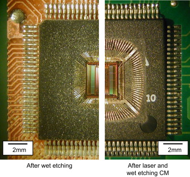
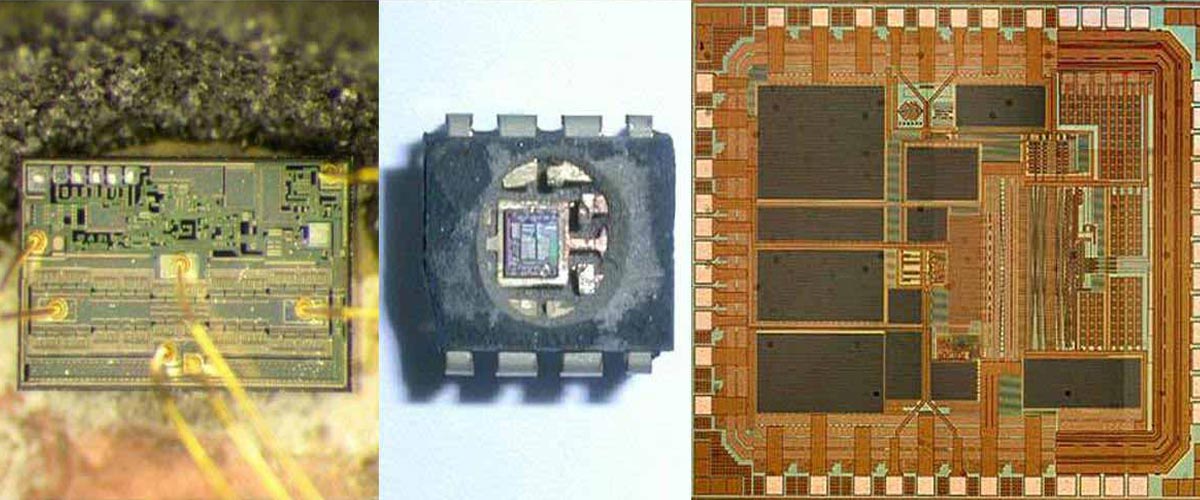
Reverse MB90F345CAPMC-GS Infineon Microcontroller Memory
Reverse MB90F345CAPMC-GS Infineon Microcontroller Memory and then clone locked microprocessor MB90F345CAP embedded firmware out from its flash memory, after attacking MCU MB90F345CAPMC protective system;
Reverse MB90F345CAPMC-GS Infineon Microcontroller Memory and then clone locked microprocessor MB90F345CAP embedded firmware out from its flash memory, after attacking MCU MB90F345CAPMC protective system;
Make sure to turn on the A/D converter power supply (AVCC, AVRH, AVRL) and analog inputs (AN0 to AN23) after turning-on the digital power supply (VCC).
Turn-off the digital power after turning off the A/D converter supply and analog inputs. In this case, make sure that the voltage does not exceed AVRH or AVCC (turning on/off the analog and digital power supplies simulta- neously is acceptable).
reverse engineering MB90F345CA INFENION sistema di protezione della memoria del microcontrollore protetto e quindi estrazione del firmware incorporato del microprocessore bloccato MB90F345CAP dalla sua memoria flash come formato di codice binario o dati essimali, dopo aver attaccato la resistenza alla manomissione MCU crittografata INFENION MB90F345CA;
The X0, X1 pins and X0A, X1A pins may be possible causes of abnormal operation. Make sure to provide bypass capacitors via the shortest distance from X0, X1 pins and X0A, X1A pins, crystal oscillator (or ceramic oscillator) and ground lines, and make sure, to the utmost effort, that the oscillation circuit lines do not cross the lines of other circuits. It is highly recommended to provide a printed circuit board art work surrounding X0, X1 pins and X0A, X1A pins with a ground area for stabilizing the operation.
For each of the mass-production products, request an oscillator evaluation from the manufacturer of the oscillator you are using. The MB90340E Series does not support internal pull-up/down resistors (except for the pull-up resistors built into ports 0 to 3). Use external components where needed. If you do not connect pins X0A and X1A to an oscillator, use pull-down handling on the X0A pin, and leave the X1A pin open.
inginerie inversă MB90F345CA INFENION securizat sistemul de protecție a memoriei microcontrolerului și apoi extrageți microprocesorul blocat MB90F345CAP firmware încorporat din memoria flash ca format de cod binar sau date heximale, după ce a atacat MCU criptat INFENION MB90F345CA rezistență la falsificare;
If PLL clock mode is selected, the microcontroller attempt to be working with the self-oscillating circuit even when there is no external oscillator or the external clock input is stopped. Performance of this operation, however, cannot be guaranteed. To prevent the internal regulator circuit from malfunctioning, set the voltage rise time during power-on to 50 ms or more (0.2 V to 2.7 V)
Reverse Engineering ST10F272M-4QR3 Encrypted Microprocessor Memory
Reverse Engineering ST10F272M-4QR3 Encrypted Microprocessor Memory can help designer to recover embedded flash content of microcontroller st10f272m-4qr3 and clone flash program in the format of binary or heximal to new MCU ST10F272M-4QR3;
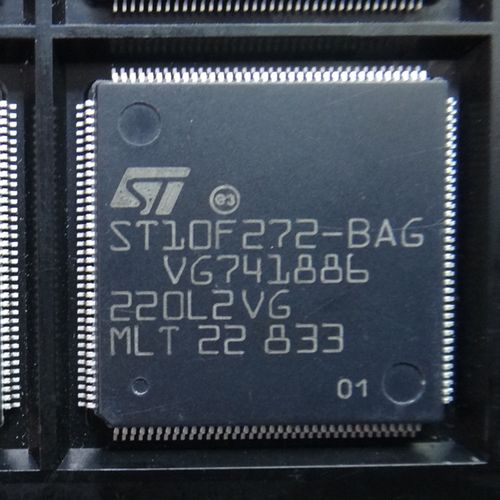
Reverse Engineering ST10F272M-4QR3 Encrypted Microprocessor Memory can help designer to recover embedded flash content of microcontroller st10f272m-4qr3 and clone flash program in the format of binary or heximal to new MCU ST10F272M-4QR3;
Output transition is not programmable.
CAN module is enhanced: ST10F273 implements two C-CAN modules, so the programming model is slightly different. Besides, the possibility to map in parallel the two CAN modules is added (on P4.5/P4.6).
On-chip main oscillator input frequency range has been reshaped, reducing it from 1 to 25 MHz down to 4 to 12 MHz. This is a low power oscillator amplifier, that allows a power consumption reduction when Real Time Clock is running in Power down mode, using as reference the on-chip main oscillator clock. When this on-chip amplifier is used as reference for Real Time Clock module, the Power-down consumption is dominated by the consumption of the oscillator amplifier itself.
зворотне проектування ST10F272M зашифрована захисна система мікропроцесора для зчитування вбудованого мікропрограмного забезпечення з флеш-пам’яті може допомогти розробнику відновити флеш-вміст двійкового файлу та шістнадцяткових даних з мікроконтролера ST10F272M
A second on-chip oscillator amplifier circuit (32 kHz) is implemented for low power modes: it can be used to provide the reference to the Real Time Clock counter (either in Power down or Stand-by mode). Pin XTAL3 and XTAL4 replace a couple of VDD/VSS pins of ST10F272M-4QR3.
visszafejtés Az ST10F272M titkosított mikroprocesszoros védelmi rendszer a beágyazott firmware flash memóriából történő kiolvasásához segíthet a tervezőnek a bináris fájlok flash tartalmának és a heximális adatoknak az ST10F272M mikrokontrollerről történő helyreállításában
8-bit bidirectional I/O port, bit-wise programmable for input or output via direction bit. Programming an I/O pin as input forces the corresponding output driver to high impedance state. Port 6 outputs can be configured as push-pull or open drain drivers. The input threshold of Port 6 is selectable (TTL or CMOS). The following Port 6 pins have alternate functions:
External access enable pin.
A low level applied to this pin during and after Reset forces the ST10F273 to start the program from the external memory space. A high level forces ST10F273 to start in the internal memory space. This pin is also used (when Stand-by mode is entered, that is ST10F273 under reset and main VDD turned off) to bias the 32 kHz oscillator amplifier circuit and to provide a reference voltage for the low-power embedded voltage regulator which generates the internal 1.8V supply for the RTC module (when not disabled) and to retain data inside the Stand-by portion of the XRAM (16Kbyte).
engenharia reversa O sistema de proteção do microprocessador criptografado ST10F272M para ler o firmware incorporado da memória flash pode ajudar o designer a recuperar o conteúdo flash do arquivo binário e dados heximais do microcontrolador ST10F272M
It can range from 4.5 to 5.5V (6V for a reduced amount of time during the device life, 4.0V when RTC and 32 kHz on-chip oscillator amplifier are turned off). In running mode, this pin can be tied low during reset without affecting 32 kHz oscillator, RTC and XRAM activities, since the presence of a stable VDD guarantees the proper biasing of all those modules.
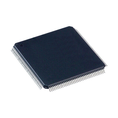
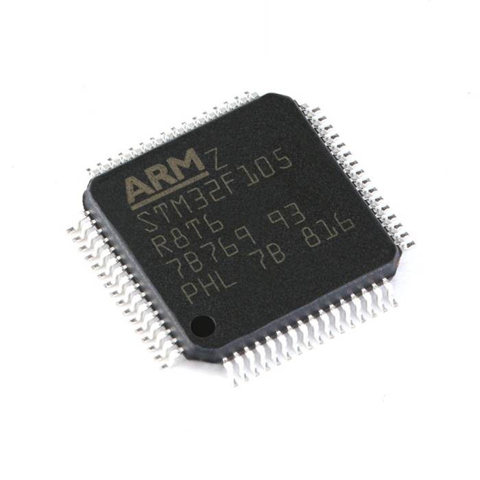
Reverse Engineer ARM STM32F105V8 Microcomputer Program
Reverse Engineer ARM STM32F105V8 Microcomputer Program can help engineer to extract source code of heximal file from secured microprocessor stm32f105v8, and then copy flash binary software to new stm32f105v8 mcu;
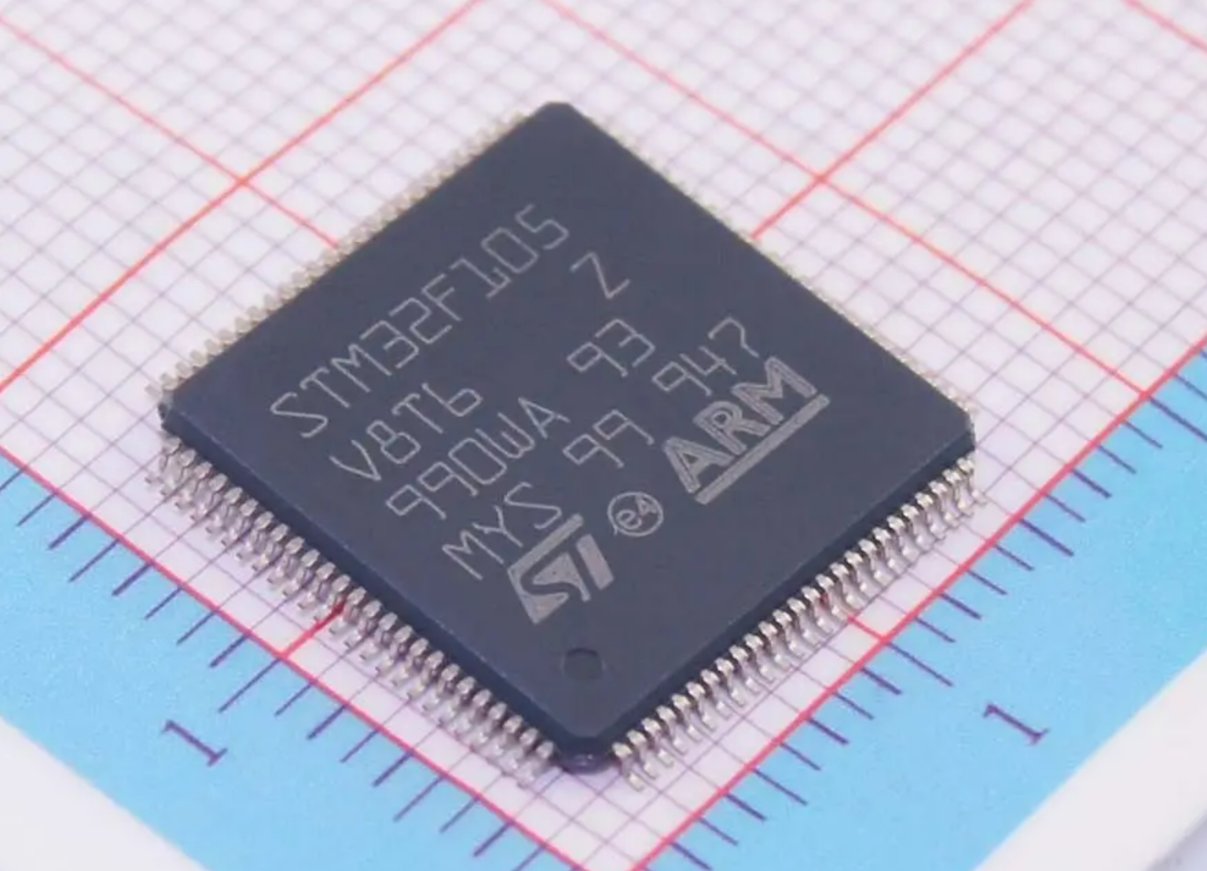
Reverse Engineer ARM STM32F105V8 Microcomputer Program can help engineer to extract source code of heximal file from secured microprocessor stm32f105v8, and then copy flash binary software to new stm32f105v8 mcu
The independent watchdog is based on a 12-bit downcounter and 8-bit prescaler. It is clocked from an independent 40 kHz internal RC and as it operates independently of the main clock, it can operate in Stop and Standby modes. It can be used either as a watchdog to reset the device when a problem occurs after replicating stm32f105r8 mcu chip embedded flash program, or as a free-running timer for application timeout management. It is hardware- or software-configurable through the option bytes. The counter can be frozen in debug mode.
The window watchdog is based on a 7-bit downcounter that can be set as free-running. It can be used as a watchdog to reset the device when a problem occurs. It is clocked from the main clock. It has an early warning interrupt capability and the counter can be frozen in debug mode.
crack locked microprocessor STM32F105V8 fuse bit and extract embedded source code from mcu chip STM32F105V8
This timer is dedicated for OS, but can be used also as a standard downcounter. It features:
- A 24-bit downcounter
- Autoreload capability
- Maskable system interrupt generation when the counter reaches 0
- Programmable clock source
Up to two I²C bus interfaces can operate in multimaster and slave modes. They can support standard and fast modes. They support dual slave addressing (7-bit only) and both 7/10-bit addressing in master mode to decrypt mcu chip stm32f105vc secured memory binary program. A hardware CRC generation/verification is embedded. They can be served by DMA and they support SM Bus 2.0/PM Bus.
descifrar el microcontrolador del brazo STM32F105V8 y extraer el firmware integrado heximal de la memoria flash
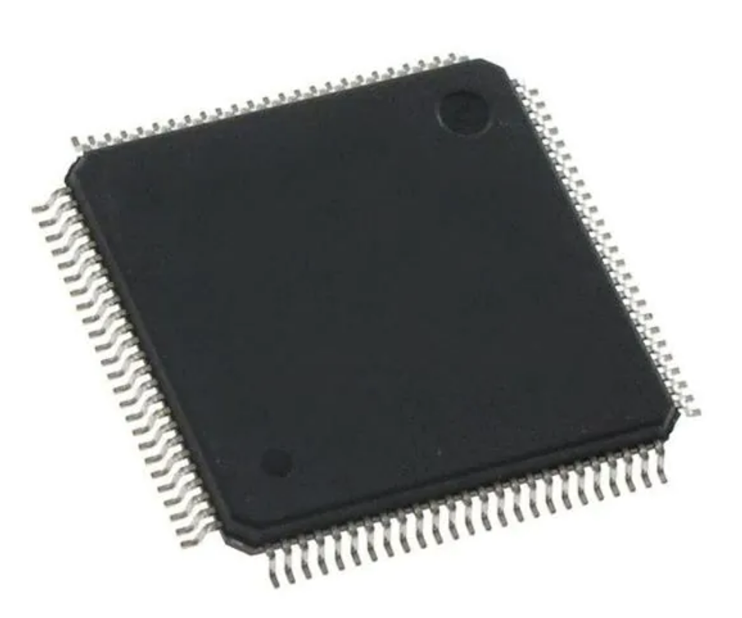
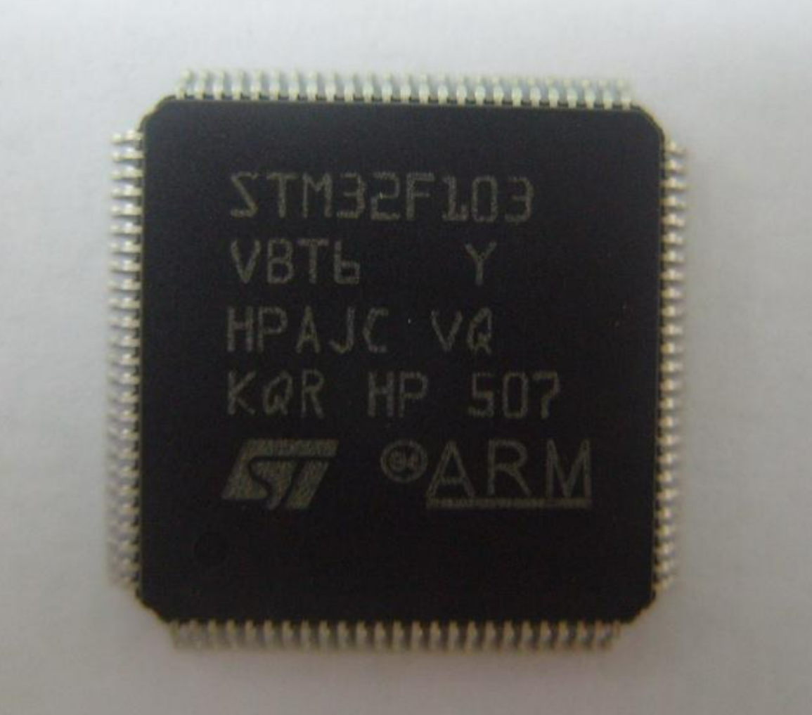
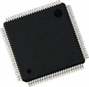
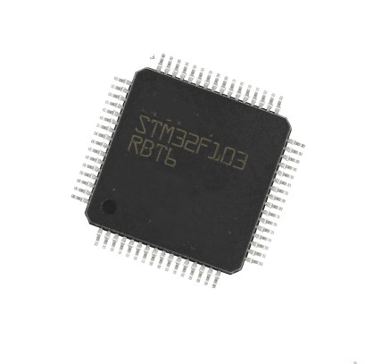
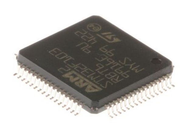
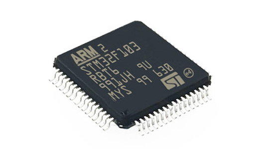
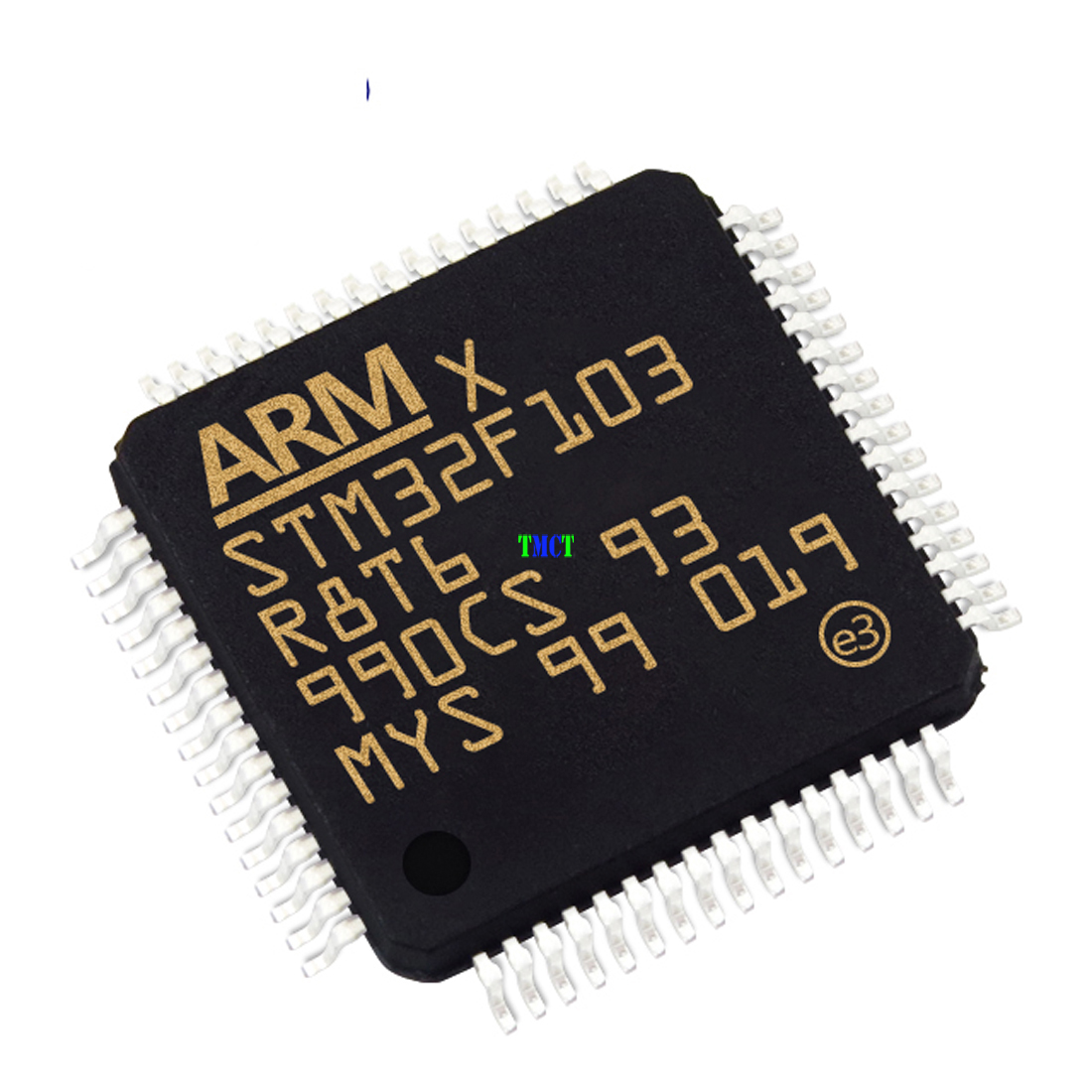
Reverse Encrypted STM32F103VB Microprocessor Protection
Reverse Encrypted STM32F103VB Microprocessor Protection and clone stm32f103vb locked mcu flash heximal file, copy flash memory firmware to arm microcontroller stm32f103vb;
Reverse Encrypted STM32F103VB Microprocessor Protection and clone stm32f103vb locked mcu flash heximal file, copy flash memory firmware to arm microcontroller stm32f103vb
The advanced-control timer (TIM1) can be seen as a three-phase PWM multiplexed on 6 channels. It has complementary PWM outputs with programmable inserted dead-times. It can also be seen as a complete general-purpose timer. The 4 independent channels can be used for
- Input capture
- Output compare
- PWM generation (edge- or center-aligned modes)
- One-pulse mode output
If configured as a general-purpose 16-bit timer, it has the same features as the TIMx timer. If configured as the 16-bit PWM generator, it has full modulation capability (0-100%).
In debug mode, the advanced-control timer counter can be frozen and the PWM outputs disabled to turn off any power switch driven by these outputs.
Many features are shared with those of the general-purpose TIM timers which have the same architecture. The advanced-control timer can therefore work together with the TIM timers via the Timer Link feature for synchronization or event chaining to recover stm32f103c6 locked mcu flash full content.
clone STMicroelectronics-STM32F103VB microprocessor flash memory content and copy embedded heximal file and binary program to new mcu chip STMicroelectronics-STM32F103VB
There are up to three synchronizable general-purpose timers embedded in the STM32F103xx performance line devices. These timers are based on a 16-bit auto-reload up/down counter, a 16-bit prescaler and feature four independent channels each for input capture/output compare, PWM or one-pulse mode output. This gives up to 12 input captures/output compares/PWMs on the largest packages.
Desbloquee el microcontrolador de brazo MCU STM32F105VBT6 y lea el firmware integrado heximal de la memoria flash
The general-purpose timers can work together with the advanced-control timer via the Timer Link feature for synchronization or event chaining. Their counter can be frozen in debug mode. Any of the general-purpose timers can be used to generate PWM outputs. They all have independent DMA request generation when recovering arm microprocessor stm32f103cb flash program.
These timers are capable of handling quadrature (incremental) encoder signals and the digital outputs from one to three Hall-effect sensors.
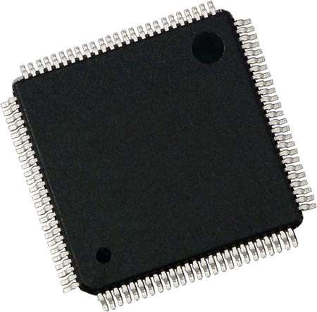
Reverse Engineering ARM Microprocessor STM32F103RB Flash Memory
Reverse Engineering ARM Microprocessor STM32F103RB Flash Memory is a process to crack stm32f103rb secured microcontroller fuse bit and copy the heximal memory firmware to new microcomputer stm32f103rb flash memory;
Reverse Engineering ARM Microprocessor STM32F103RB Flash Memory is a process to crack stm32f103rb secured microcontroller fuse bit and copy the heximal memory firmware to new microcomputer stm32f103rb flash memory
The device has an integrated power-on reset (POR) / power-down reset (PDR) circuitry. It is always active, and ensures proper operation starting from/down to 2 V to pull out stm32f103t8 microcontroller flash data. The device remains in reset mode when VDD is below a specified threshold, VPOR/PDR, without the need for an external reset circuit.
The device features an embedded programmable voltage detector (PVD) that monitors the VDD/VDDA power supply and compares it to the VPVD threshold. An interrupt can be generated when VDD/VDDA drops below the VPVD threshold and/or when VDD/VDDA is higher than the VPVD threshold. The interrupt service routine can then generate a warning message and/or put the MCU into a safe state. The PVD is enabled by software.
unlock STM32F103RB arm microcontroller fuse bit and readout firmware heximal of flash memory of mcu stm32f103rb
The regulator has three operation modes: main (MR), low-power (LPR) and power down.
- MR is used in the nominal regulation mode (Run)
- LPR is used in the Stop mode
- Power down is used in Standby mode: the regulator output is in high impedance: the kernel circuitry is powered down, inducing zero consumption (but the contents of the registers and SRAM are lost)
This regulator is always enabled after reset. It is disabled in Standby mode, providing high impedance output. The STM32F103xx performance line supports three low-power modes to achieve the best compromise between low-power consumption, short startup time and available wakeup sources:
- Sleep mode
In Sleep mode, only the CPU is stopped. All peripherals continue to operate and can wake up the CPU when an interrupt/event occurs.
- Stop mode
The Stop mode achieves the lowest power consumption while retaining the content of SRAM and registers. All clocks in the 1.8 V domain are stopped by cracking stm32f103vet7 arm ic mcu flash memory, the PLL, the HSI RC and the HSE crystal oscillators are disabled. The voltage regulator can also be put either in normal or in low-power mode.
desbloquee la broca del fusible del microcontrolador del brazo STM32F103RB y lea el firmware heximal de la memoria flash de mcu stm32f103rb
Reverse Engineering STM32F103R8 Microcomputer Flash Program
Reverse Engineering STM32F103R8 Microcomputer Flash Program can help engineer to extract embedded firmware heximal file from secured mcu stm32f103r8 then clone arm microcontroller stm32f103r8 binary data to new Microprocessor;
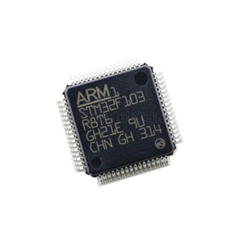
Reverse Engineering STM32F103R8 Microcomputer Flash Program can help engineer to extract embedded firmware heximal file from secured mcu stm32f103r8 then clone arm microcontroller stm32f103r8 binary data to new Microprocessor
System clock selection is performed on startup, however the internal RC 8 MHz oscillator is selected as default CPU clock on reset. An external 4-16 MHz clock can be selected, in which case it is monitored for failure. If failure is detected, the system automatically switches back to the internal RC oscillator when restoring stm32f103c4 arm microcontroller flash binary file. A software interrupt is generated if enabled. Similarly, full interrupt management of the PLL clock entry is available when necessary (for example on failure of an indirectly used external crystal, resonator or oscillator).
Several prescalers allow the configuration of the AHB frequency, the high-speed APB (APB2) and the low-speed APB (APB1) domains. The maximum frequency of the AHB and the high-speed APB domains is 72 MHz. The maximum allowed frequency of the low-speed APB domain is 36 MHz. See Figure 2 for details on the clock tree.
unlock secured STM32F105R8T6 microcontroller fuse bit and extract heximal program file from STM32F105R8T6 microprocessor flash memory
At startup, boot pins are used to select one of three boot options:
- Boot from user Flash
- Boot from System memory
- Boot from embedded SRAM
The boot loader is located in System memory. It is used to reprogram the Flash memory by using USART1. For further details refer to AN2606, available on www.st.com.
- VDD = 2.0 to 3.6 V: external power supply for I/Os and the internal regulator. Provided externally through VDD
- VSSA, VDDA = 2.0 to 3.6 V: external analog power supplies for ADC, reset blocks, RCs and PLL (minimum voltage to be applied to VDDA is 2.4 V when the ADC is used) by restoring stm32f103c8 microcontroller flash program code. VDDA and VSSA must be connected to VDD and VSS,
- VBAT = 8 to 3.6 V: power supply for RTC, external clock 32 kHz oscillator and backup registers (through power switch) when VDD is not present.
For more details on how to connect power pins, refer to Figure 14: Power supply scheme.
El programa flash de microcomputadora STM32F103R8 de ingeniería inversa puede ayudar al ingeniero a extraer el archivo heximal del firmware integrado de mcu stm32f103r8 seguro y luego clonar los datos binarios del microcontrolador stm32f103r8 del brazo al nuevo microprocesador
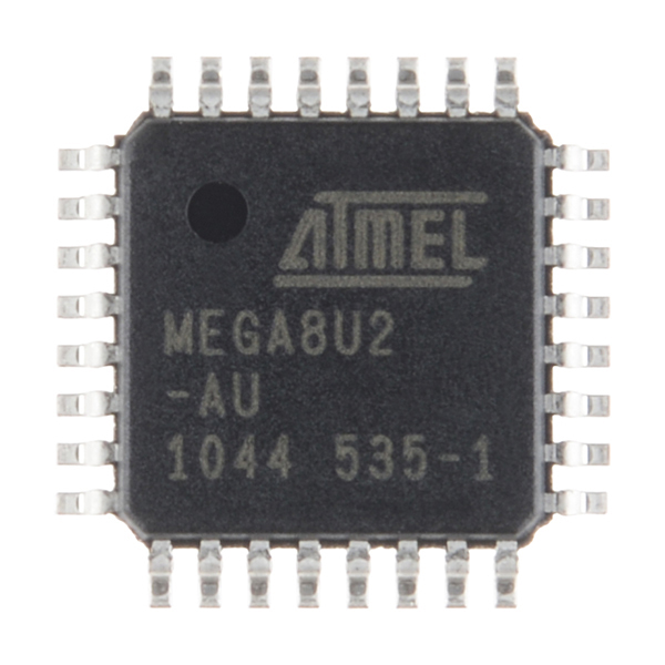
Reverse AVR Microcomputer ATmega16U2 Flash Program
Reverse AVR Microcomputer ATmega16U2 Flash Program and copy atmel avr mcu atmega16u2 firmware to new microcontroller, the heximal firmware of original atmega16u2 microprocessor can be restored;
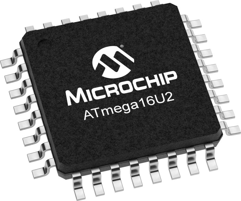
Reverse AVR Microcomputer ATmega16U2 Flash Program and copy atmel avr mcu atmega16u2 firmware to new microcontroller, the heximal firmware of original atmega16u2 microprocessor can be restored
The ATmega8U2/16U2/32U2 are supported with a full suite of program and system develop- ment tools including: C compilers, macro assemblers, program debugger/simulators, in-circuit emulators, and evaluation kits.
AVCC is the supply voltage pin (input) for all analog features (Analog Comparator, PLL). It should be externally connected to VCC through a low-pass filter.
Port B is an 8-bit bi-directional I/O port with internal pull-up resistors (selected for each bit). The Port B output buffers have symmetrical drive characteristics with both high sink and source capability. As inputs, Port B pins that are externally pulled low will source current if the pull-up resistors are activated. The Port B pins are tri-stated when a reset condition becomes active, even if the clock is not running.
crack secured mcu ATMEGA8U2
Port B also serves the functions of various special features of the ATmega8U2/16U2/32U2 as listed on page 74. Port D serves as analog inputs to the analog comparator.
Port D also serves as an 8-bit bi-directional I/O port, if the analog comparator is not used (con- cerns PD2/PD1 pins). Port pins can provide internal pull-up resistors (selected for each bit). The Port D output buffers have symmetrical drive characteristics with both high sink and source capability. As inputs, Port D pins that are externally pulled low will source current if the pull-up resistors are activated. The Port D pins are tri-stated when a reset condition becomes active, even if the clock is not running.
Reset input. A low level on this pin for longer than the minimum pulse length will generate a reset, even if the clock is not running. The minimum pulse length is given in “System Control and Reset” on page 47. Shorter pulses are not guaranteed to generate a reset. This pin alternatively serves as debugWire channel or as generic I/O. The configuration depends on the fuses RST- DISBL and DWEN.