Archive for the ‘PCB Assembly’ Category
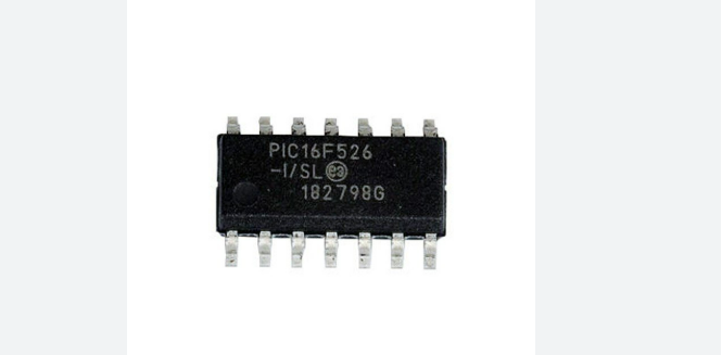
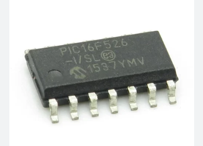
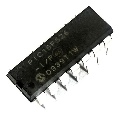
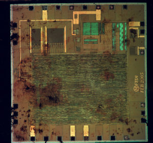
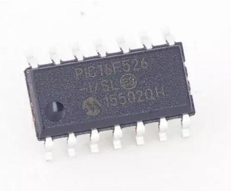
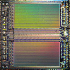
 Reverse Engineering Microcontroller PIC16F526 Binary
Reverse engineering the binary of a microcontroller, such as the PIC16F526, is a process used to break down or crack the firmware and software embedded within the device. This technique is often applied in a variety of fields, from security analysis to legacy system restoration. In this article, we will explore how reverse engineering works on the PIC16F526 microcontroller and the key steps involved in recovering protected or encrypted software.
What is Reverse Engineering a PIC16F526?
Reverse engineering a microcontroller like the PIC16F526 involves extracting and decoding the firmware stored in the device’s flash memory or EEPROM memory. The main goal is to recover or restore the source code that controls the microcontroller’s behavior. Often, this binary is encrypted or locked to prevent unauthorized access, making it challenging to directly access the program or heximal data.
Breaking the Protection
One of the key challenges when reverse engineering the PIC16F526 binary is dealing with protected firmware. Manufacturers often encrypt the software or firmware to prevent attackers from gaining access to proprietary code or system secrets. To decrypt the firmware, attackers might use various techniques, such as attacking the microcontroller’s security features, exploiting hardware vulnerabilities, or using software-based tools that can bypass security measures.
Обратное проектирование двоичного кода микроконтроллера, такого как PIC16F526, представляет собой процесс, используемый для взлома встроенного в устройство программного обеспечения и прошивки. Этот метод часто применяется в различных областях: от анализа безопасности до восстановления устаревших систем. В этой статье мы рассмотрим, как работает обратное проектирование на микроконтроллере PIC16F526, а также основные этапы восстановления защищенного или зашифрованного программного обеспечения.
Extracting the Binary
Once the protection is bypassed, the next step is to extract the binary code stored in the flash memory. Specialized tools can read the heximal data from the microcontroller’s memory and output it in a usable format. At this point, the binary may need to be decoded to understand its structure, as it could include encrypted or obfuscated data. Software such as disassemblers or decompilers may be used to decode the binary into an intermediate assembly code or even reconstruct the source code in higher-level languages.
Recovering and Modifying the Program
In cases where the goal is to restore or update the program, engineers may modify the source code after reverse engineering the microcontroller. This is common in situations where legacy systems need upgrading or customization, and the original source code is no longer available. Once modifications are made, the new firmware can be reflashed back into the microcontroller, restoring the updated functionality.
مهندسی معکوس باینری یک میکروکنترلر، مانند PIC16F526، فرآیندی است که برای خراب کردن یا شکستن سفتافزار و نرمافزار تعبیهشده در دستگاه استفاده میشود. این تکنیک اغلب در زمینه های مختلفی از تجزیه و تحلیل امنیتی گرفته تا بازیابی سیستم قدیمی استفاده می شود. در این مقاله، نحوه عملکرد مهندسی معکوس بر روی میکروکنترلر PIC16F526 و مراحل کلیدی مربوط به بازیابی نرم افزارهای محافظت شده یا رمزگذاری شده را بررسی خواهیم کرد.
Applications of Reverse Engineering PIC16F526
Reverse engineering the PIC16F526 binary can serve multiple purposes. It’s often used to analyze system vulnerabilities, recover lost or inaccessible firmware, and enhance system performance. In some cases, this process is also crucial in understanding how a device works, for example, in cracking a proprietary algorithm or unlocking hidden features.
Conclusion
Reverse engineering the binary of a microcontroller like the PIC16F526 is a powerful tool for developers, security analysts, and engineers. By using techniques to break protections, decrypt encrypted data, and recover the original source code, the process enables greater flexibility in working with hardware. However, the ethical and legal considerations surrounding reverse engineering should always be taken into account, as unauthorized cracking or modifying of software can have legal ramifications.
We can Reverse engineering Microcontroller PIC16F526 Binary, please view the Microcontroller PIC16F526 features for your reference:
High-Performance RISC CPU:
· Only 33 Single-Word Instructions
· All Single-Cycle Instructions except for Program Branches which are Two-Cycle
· Two-Level Deep Hardware Stack
· Direct, Indirect and Relative Addressing modes for Data and Instructions
· Operating Speed:
– DC – 20 MHz crystal oscillator
– DC – 200 ns instruction cycle
· On-chip Flash Program Memory:
– 1024 x 12
· General Purpose Registers (SRAM):
– 67 x 8
restoring PIC16F526 locked MCU heximal program
· Flash Data Memory:
– 64 x 8
Special Microcontroller Features:
· 8 MHz Precision Internal Oscillator when Break IC PIC16F610 Binary
– Factory calibrated to ±1%
· In-Circuit Serial Programming™ (ICSP™)
· In-Circuit Debugging (ICD) Support
· Power-On Reset (POR)
· Device Reset Timer (DRT)
· Watchdog Timer (WDT) with Dedicated On-Chip RC Oscillator for Reliable Operation
· Programmable Code Protection
· Multiplexed MCLR Input Pin
· Internal Weak Pull-ups on I/O Pins
· Power-Saving Sleep mode
PIC16F526 microcontroller embedded heximal file recovery
· Wake-Up from Sleep on Pin Change
· Selectable Oscillator Options:
– INTRC: 4 MHz or 8 MHz precision Internal RC oscillator
– EXTRC: External low-cost RC oscillator
– XT: Standard crystal/resonator
– HS: High-speed crystal/resonator
– LP: Power-saving, low-frequency crystal
– EC: High-speed external clock input
Reverse Engineering Microcontroller PIC16F526 Binary
Low-Power Features/CMOS Technology:
· Standby current:
– 100 nA @ 2.0V, typical
· Operating current:
– 11 mA @ 32 kHz, 2.0V, typical
– 175 mA @ 4 MHz, 2.0V, typical
· Watchdog Timer current:
– 1 mA @ 2.0V, typical
– 7 mA @ 5.0V, typical
· High Endurance Program and Flash Data Memory cells:
– 100,000 write Program Memory endurance to Recover MCU 12F508 Code
– 1,000,000 write Flash Data Memory endurance
– Program and Flash Data retention: >40 years
· Fully Static Design
· Wide Operating Voltage Range: 2.0V to 5.5V:
– Wide temperature range
– Industrial: -40°C to +85°C
– Extended: -40°C to +125°C
Peripheral Features:
· 12 I/O Pins:
– 11 I/O pins with individual direction control
– 1 input-only pin
– High current sink/source for direct LED drive
– Wake-up on change
– Weak pull-ups
· 8-bit Real-time Clock/Counter (TMR0) with 8-bit Programmable Prescaler
การวิศวกรรมย้อนกลับไบนารีของไมโครคอนโทรลเลอร์ เช่น PIC16F526 เป็นกระบวนการที่ใช้ในการทำลายหรือแคร็กเฟิร์มแวร์และซอฟต์แวร์ที่ฝังอยู่ในอุปกรณ์ เทคนิคนี้มักใช้ในหลากหลายสาขา ตั้งแต่การวิเคราะห์ความปลอดภัยไปจนถึงการกู้คืนระบบเก่า ในบทความนี้ เราจะสำรวจวิธีการทำงานของวิศวกรรมย้อนกลับบนไมโครคอนโทรลเลอร์ PIC16F526 และขั้นตอนสำคัญที่เกี่ยวข้องกับการกู้คืนซอฟต์แวร์ที่ได้รับการป้องกันหรือเข้ารหัส
· Two Analog Comparators:
– Comparator inputs and output accessible externally
– One comparator with 0.6V fixed on-chip absolute voltage reference (VREF) by Unlock Microcontroller
– One comparator with programmable on-chip voltage reference (VREF)
· Analog-to-Digital (A/D) Converter:
– 8-bit resolution
– 3-channel external programmable inputs
– 1-channel internal input to internal absolute 0.6 voltage reference
PIC16F526 microprocessor flash program code replication
Introduction of Flexible Circuit Assembly
Flexible circuits offer some unique challenges to the assembly process. The assembly materials and processes for populating and interconnecting components to a flexible circuit range are essentially identical to those used for standard rigid or rigid flex pcb, but there are some twists required, as will be shown. The assembly processes range from very simple methods, such as manual component insertion and hand soldering (which requires little or no fixturing), to fully automated methods, which normally require specially developed, design-specific and dedicated fixtures.
How, then, does one choose an assembly process and method for flexible circuits? To begin appropriately, it is necessary to consider a number of important factors: What is the flexible circuit base material? What types of components will be used? How many assemblies will be built? These and other important questions must be addressed before one can adequately make the proper decisions regarding assembly. These seemingly simple matters can greatly influence the pcb assembly choice. For example, it is commonly assumed that polyester circuits cannot be used in applications where soldering is required. The reason for this assumption is that polyester films have a low melt point and will be grossly distorted by the tin-lead soldering process. However, when properly fixtured, soldering can be used for joining components to polyester. A number of major OEMs have been doing just that for many years. They have developed methods that provide proper shielding of the body of the polyester circuit in process. The distortion of the material can be localized to areas adjacent to the point of connection.
With the advent of the well-meant but misguided legislation mandating the use of lead-free solders, there will be significant challenges ahead, as lead-free solders have a roughly 30-40ºC higher melting temperature than traditional tin-lead solders. Sadly, it appears that traditional tin-lead solders are actually more environmentally friendly, so the law does double damage. One alternative is to use lower-temperature solders, or conductive adhesives can also be employed. The important thing is that manufacturers not limit themselves in their thinking and that they be open to alternative solutions. Following is a brief review of the key elements of flex circuit assembly.
Dual probe and Flying probe test
Flying probe doesn’t rely on the pin drawing fixed on fixture. Two or more probes can be installed on the surface of X-Y and move freely, the testing point can be controlled by CAD GERBER FILE. Dual probe can move within 4 mil area. Probe can move isolated, also at the same time didn’t restrict the real distance of how close they can be. Testing device with 2 moving hands is base upon capacitor, press PCB on the insulation layer of a metal sheet as the capacitor for another metal sheet. In case there is 1 wire happen to short, capacitor value will become larger then certain point; if there is a open wire, capacitor will become smaller.
Inspection technology of PCB 1
With the development of surface mount technology, the mounting density of PCB is increasing very fast, as a result of that, even for PCB with less density, automatic inspection is not only basic requirement, but also commercial. During the inspection for complex PCB inspection, 2 normal ways are nail-bed test and flying probe test.
1 Nail-bed test
This kind of way is using probe with spring to connect with each test point on the PCB. Spring can let the probe withstand 100-200gpress force and to ensure each test point working properly, all the nail probe array together can be viewed as nail bed. Under the control of inspection software, we can program test point and test signal, graphic below is a typical structure of nail bed inspection, inspector can acquire all the information about test point. Although both side of PCB can be tested simultaneously by using nail-bed test method, designer should still consider to install all the test point on the solder side of PCB. Nail-bed test device is very expensive and hard to repair.

There is basic universal array processor constitute by drilled bare board, the distance among each pin center is 100mil, 75mil and 50mil. These pins play the role like probe, and use electrical connector or joint on the PCB to make mechanic communication. If PAD on PCB is compatible with test array, then polyamide film which has been drilled orderly can be placed among them for the sake of inspection design. Continual inspection is through get access to end point of network grid. Since all the networks on the PCB can execute continually inspection, then a isolated inspection can be finished. However the distance of each probe constrain the functionality of each nail-bed.
The best way of Printed Circuit Board Welding
1 Wetting
When the hot and liquid soldering tin dissolve and penetrate onto the surface of metal, it can be defined as metal wetting. Molecule of mixture of soldering tin and copper can form a new alloy which contains part of copper and part of soldering tin. Molecule bond is the core of welding, it can decide the hardness and quality of soldering point, wetting can take place only on the copper surface which has not yet being contaminated, no oxide film due to exposure under air, at the same time, temperature should reach certain level.
2 Surface tension
Everyone knows the surface tension on the water, this tension can keep the cold water drop remain the same shape on the metal plate with grease, this is because adhesion which tend to make upper liquid expansion on the surface is smaller than its cohesion. Use warm water and cleanser can reduce the surface tension, water can soak the metal plate with grease and flow out to form a thin film, if the adhesion is bigger than cohesion will occur this situation.
Cohesion of TIN-LEAD soldering tin is even bigger than water, which can make the soldering tin as ball shape which can help to minimize the surface size, to satisfy minimum energy state requirement. Flux play the role as cleanser to metal plate with grease, additional, surface tension is highly depends on the cleaning level and temperature, only adhesion power is much greater than cohesion power, reasonable wetting can occur.
3 Alloy metal
Metallic bond among copper and tin can form grain, the shape and size of grain are determined by soldering temperature and lasting time length, hardness. Less heat during soldering can form more deliberate poikilitic texture, to form the best soldering point with hardest strength. Too much reaction time, either extremely time length of soldering or overheat or both will cause crude poikilitic texture.
What is PCB Soldering?
Soldering is a kind of process through which the metal parts being connected by different kinds of alloy soldering tin. So the parts are capable of connected through surface molecule on the pretext of not being melted.

Soldering include SOFT and HARDEN, temperature of soft soldering below 450℃, temperature of harden soldering above 450℃. Harden Soldering usually be applied on silver, gold, steel and copper, it is soldering point is much more fastness than SOFT soldering, shearing strength is 20-30 times than SOFT soldering, these 2 heat-connecting mentioned above are all using SOLDERING, because the fundamental principle of both soldering methods are all inject the molten soldering tin into the long and narrow aperture of two clean surface of components.

Soldering ensure continuity of metal. First, if two metals connected with each other through bolt connection or physical adhesion, although it can be viewed as a compact integer, but this connection is discontinuous, sometimes if there is an oxidation-insulation film, then they aren’t even physical connection. Another drawback of mechanical connection compare with soldering is if the contact space keep on oxidation will increase the resistance value. Besides, vibration and other mechanical shock will loose the bolt. Soldering can eliminate these problems, soldering locations won’t have relative displacement, contact area won’t oxidize which can help to maintain continue conduction route. Soldering is a process during which 2 metal melted and combine with each other. When soldering tin in the state of molten, it can melt the metal where is being contacted by it, most of the time there could be a very thin oxidation film on the surface of soldering tin covered metal, flux hereby will play the role of melting this oxidation film. Soldering process normally includes:

1> Flux melt down which can help to strip off the oxidation film on the surface of metal;
2> Melt the soldering tin to make the impurity and lighter flux can float onto the surface;
3> Melt partly the metal which has connection with soldering tin;
4> Cold down and finish the fusion process.

PCB Repair need to orient root cause in the circuit board, so usually need to dissemble components from circuit board and do the necessary test and measurement, this process will include:
1> Dissemble special components;
2> Component test;
3> Replace those defected components;
4> Inspect circuit pattern functions;
Dissemble and replace other components will need to instruct soldering procedure.

What is electronic PCB
PCB (Printed Circuit Board): It appears in almost every electronic device. If there exist electronic components a certain kind of equipment, which are set in various sizes of PCB. In addition to fix a variety of small parts, the main function of PCB is to provide electrical connections among the parts. As electronic devices become more complexity which requiring more and more electronic components, the intensity of circuit pattern and electronic parts on the PCB are also increasing simultaneously. Bare board (without any electronic components on it) is also often referred to as “Printed Wiring Board (PWB) “. The substrate of PCB is composed of insulated as well as non-pliable material. Small circuit wire as you can on the surface of laminate is copper foil, copper foil is covered on the surface of raw laminate, and being etched away in the manufacturing process, those part being left behind as a network of fine lines form the circuit pattern. These lines are called conductors (conductor pattern) or said wiring, which are used to provide electrical connections on the PCB for those components.
Several Commonly Used Standards refers to Electronic Manufacture (1)
1> IPC-ESD-2020: United Standard, developed by electrostatic discharge control programme, includes all the necessary design, establishment, installation and maintenance of electrostatic discharge programme. According to the history experience of some military and commercial organization, provide guidance of solution and protection during sensitive period of electrostatic discharge.
2> IPC-AC-62A: Handbook of water clearing after assembly, describe composition of residue and remains, type and feature of cleanser, process of clearing, related equipment and technology, quality control, environment control and employee safety, method of verify the level of clearness and charge of clearing.
3> IPC-DRM-4 9 0E: Evaluation Reference Manual of THROUGH-HOLE soldering point. Describe the components, hole-wall and soldering PAD coverage specification according to the standard in details. Except that, also include the 3D drawing created by computer, include tin filled, contact lead, contact tin, vertical filled and solder PAD cover and lots of soldering points defects.
4> IPC-TA-722: Appraisal Handbook of soldering technology. 45 articles refer to each aspect of soldering technology, content refers to normal soldering, soldering material, manual soldering, soldering in big volume, wave soldering, reflow soldering, vapor phase soldering and infrared soldering.
5> IPC-7525: Template Design Directory. Provide guidelines for design and manufacture of stencil used as template of solder and surface mount bonder, also discuss template design for the application of surface mount technology, introduce hybrid-technology of thru-hole and upside-down chip mounting, include overprint, mackle and stagewise template design.
6> IPC/EIA J-STD-004: Requirement Specification of Flux, include the qualification and category of colophony, resin, Classify organic and Inorganic flux according to the amount of halide and activation level; also include the usage of flux, material which contain flux and no-residue flux when apply in the no-clean process.
7> IPC/EIA J-STD-005: Soldering Paste Specification, list characters of soldering paste and qualification requirement, also include testing method and metal content standard, as well as stickiness, roughness, solder ball, glutinosity, and wetting capability of solder paste.
How to check Printed Circuit Board Assembly
A wide variety of inspection equipment has been invented in order to fulfill the task of Printed Circuit Board Inspection. Automatic Optical Inspection (AOI) is mainly applied on the inner layer inspection before outer layer Printed Circuit Board being laminated onto it. After lamination, X-Ray monitoring system being used to inspect the preciseness of layer-to-layer alignment and minor defect; Laser scanning system can help to inspect PAD before reflow soldering. All the methods mention above plus visual inspection on-site as well as automatic pick & place machine can effectively ensure the stability of final assembly and PCBA.

However, final inspection upon Printed Circuit Board Assembly is indispensable even if all the efforts be made; maybe it is the most critical step because it is the final unit for product and process evaluation.
Final inspection of Printed Circuit Board Assembly can be executed through manual method or automatic system, and most of time these 2 methods should be instructed simultaneously, MANUALLY means one operator inspect Printed Circuit Board Assembly visually through visual tool in hand and make the right judgment about the defect on the Printed Circuit Board Assembly. Automatic system use computer assistant drawing analyzing method to spot the defect; people also thinks that automatic system include all the inspection methods except manually visual inspection.

X-Ray technology provides a method which can help to assess the thickness, dissipation, cavity, crack, loose weld. Ultrasonic can inspect cavity, crack and break lead. AOI can assess cosmetic features, such as bridge-connection, tin volume and shape. Laser inspection can provide 3D pictures for cosmetic features. Infrared inspection can compare an existing good quality soldering point with the inspected location, through the thermal signal difference can find the inner defect of soldering points.
There is another important point, we have already known that all the automatic inspection technology can’t spot all the defects on the Printed Circuit Board Assembly. So manual visual inspection combine with automatic inspection could effectively solve this problem especially for those small quantity application. X-Ray inspection plus manual visual inspection could be the best combination of Printed Circuit Board Assembly inspection method.
Below are the main defects which has shown the highest frequency of existence on the Printed Circuit Board Assembly:
1) Component Missing;
2) Component Defect;
3) Miss registration of component;
4) Component invalidation;
5) Poor Soldering;
6) Bridge joint;
7) Insufficient soldering;
8) Tin ball;
9) Pin hole;
10) Residue;
11) Unsuitable PAD;
12) Polar upside down;
13) Lead lift;
14 ) Over length lead;
15) Cold soldering;
16) Abundant solder tin;
Break IC PIC12HV615 Heximal
Break IC PIC12HV615 Heximal
We can Break IC PIC12HV615 Heximal, please view the IC PIC12HV615 features for your reference:
To read a program memory location, the user must write two bytes of the address to the PMADRL and PMADRH registers, and then set control bit RD (PMCON1<0>). Once the read control bit is set, the program memory Flash controller will use the second instruction cycle after to read the data.
This causes the second instruction immediately following the “BSF PMCON1,RD” instruction to be ignored. The data is available in the very next cycle in the PMDATL and PMDATH registers; it can be read as two bytes in the following instructions.
PMDATL and PMDATH registers will hold this value until another read or until it is written to by the user (during a write operation). A word of the Flash program memory may only be written to if the word is in an unprotected segment of memory after Break IC.
Flash program memory must be written in four-word blocks. See Figure 3-2 and Figure 3-3 for more details. A block consists of four words with sequential addresses, with a lower boundary defined by an address, where PMADRL<1:0> = 00. All block writes to program memory are done as 16-word erase by four-word write operations. The write operation is edge aligned and cannot occur across boundaries. To write program data, it must first be loaded into the buffer registers (see Figure 3-2). This is accomplished by first writing the destination address to PMADRL and PMADRH and then writing the data to PMDATL and PMDATH.
After the address and data have been set up, then the following sequence of events must be executed:
Write 55h, then AAh, to PMCON2 (Flash programming sequence). Set the WR control bit of the PMCON1 register. All four buffer register locations should be written to with correct data. If less than four words are being written to in the block of four words, then a read from the program memory location(s) not being written to must be performed if Break IC.
This takes the data from the program location(s) not being written and loads it into the PMDATL and PMDATH registers. Then the sequence of events to transfer data to the buffer registers must be executed. To transfer data from the buffer registers to the program memory, the PMADRL and PMADRH must point to the last location in the four-word block (PMADRL<1:0> = 11). Then the following sequence of events must be executed:
Write 55h, then AAh, to PMCON2 (Flash programming sequence). Set control bit WR of the PMCON1 register to begin the write operation. The user must follow the same specific sequence to initiate the write for each word in the program block, writing each program word in sequence (000, 001, 010, 011). When the write is performed on the last word (PMADRL<1:0> = 11), a block of sixteen words is automatically erased and the content of the four-word buffer registers are written into the program memory. After the “BSF PMCON1,WR” instruction, the processor requires two cycles to set up the erase/write operation. The user must place two NOP instructions after the WR bit is set. Since data is being written to buffer registers, the writing of the first three words of the block appears to occur immediately before Break IC.