Archive for the ‘Break IC’ Category
 Break Chip ATmega48PA Heximal
 July 16th, 2014 |
  Author:
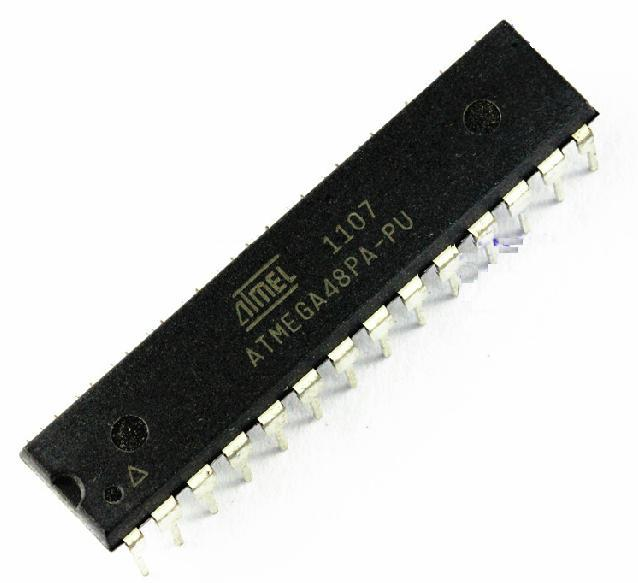
 Break Chip ATmega48PA Heximal is a focused embedded firmware recovery service created for authorized projects where access to original program files has been lost or restricted. The ATmega48PA is a compact and efficient AVR microcontroller widely used in consumer electronics, smart sensors, industrial control modules, lighting systems, small appliances, and low-power embedded products. Thanks to its stable architecture, low energy consumption, and flexible peripherals, this chip is often selected for long-lifecycle designs that must remain operational for many years.
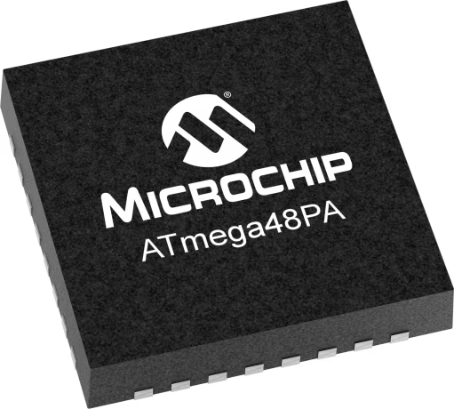
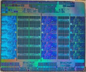
From a technical perspective, the ATmega48PA integrates flash memory, EEPROM, SRAM, and multiple I/O and communication functions into a single embedded platform. To safeguard intellectual property, many manufacturers enable protective, protected, locked, or encrypted configurations that restrict access to firmware, binary, or heximal data. While these mechanisms are effective during mass production, they can become obstacles during maintenance, redesign, or product duplication. Our Break Chip ATmega48PA Heximal service is intended to help clients attack and break these barriers in a controlled, professional context, enabling the retrieval of embedded program archives when legitimate business needs arise.
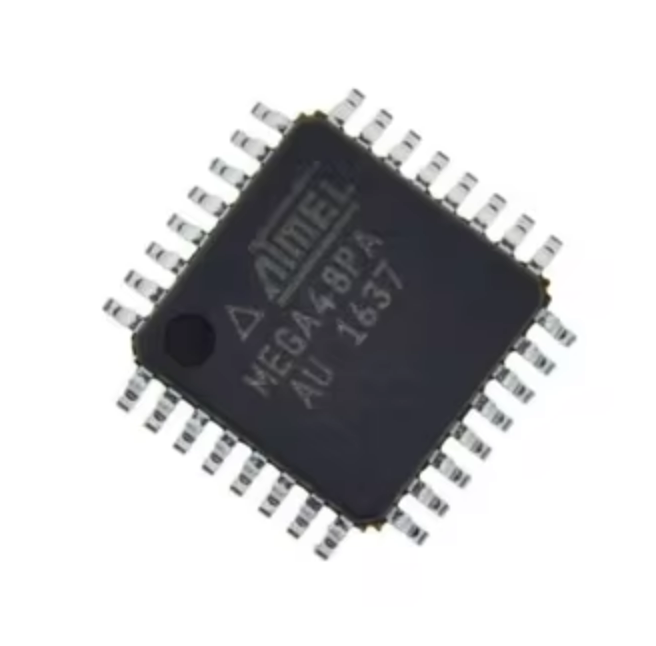
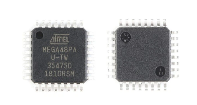
We can Break Chip ATMEGA48PA Heximal, please view below Chip ATMEGA48PA Features for your reference:
· High Performance, Low Power AVR® 8-Bit Microcontroller
· Advanced RISC Architecture
– 131 Powerful Instructions – Most Single Clock Cycle Execution
– 32 x 8 General Purpose Working Registers
– Fully Static Operation
– Up to 20 MIPS Throughput at 20 MHz
– On-chip 2-cycle Multiplier
– 4/8/16/32K Bytes of In-System Self-Programmable Flash progam memory (ATmega48PA/88PA/168PA/328P)
– 256/512/512/1K Bytes EEPROM (ATmega48PA/88PA/168PA/328P)
– 512/1K/1K/2K Bytes Internal SRAM (ATmega48PA/88PA/168PA/328P)
– Write/Erase Cycles: 10,000 Flash/100,000 EEPROM
– Data retention: 20 years at 85°C/100 years at 25°C(1)
– Optional Boot Code Section with Independent Lock Bits
In-System Programming by On-chip Boot Program
True Read-While-Write Operation
– Programming Lock for Software Security
Peripheral Features
– Two 8-bit Timer/Counters with Separate Prescaler and Compare Mode
– One 16-bit Timer/Counter with Separate Prescaler, Compare Mode, and Capture Mode
– Real Time Counter with Separate Oscillator
– Six PWM Channels
– 8-channel 10-bit ADC in TQFP and QFN/MLF package
Temperature Measurement
– 6-channel 10-bit ADC in PDIP Package
Temperature Measurement
– Programmable Serial USART
– Master/Slave SPI Serial Interface
– Byte-oriented 2-wire Serial Interface (Philips I2C compatible)
– Programmable Watchdog Timer with Separate On-chip Oscillator
– On-chip Analog Comparator
– Interrupt and Wake-up on Pin Change
Special Microcontroller Features
– Power-on Reset and Programmable Brown-out Detection
– Internal Calibrated Oscillator
– External and Internal Interrupt Sources
– Six Sleep Modes: Idle, ADC Noise Reduction, Power-save, Power-down, Standby, and Extended Standby I/O and Packages
– 23 Programmable I/O Lines
– 28-pin PDIP, 32-lead TQFP, 28-pad QFN/MLF and 32-pad QFN/MLF
Operating Voltage:
– 1.8 – 5.5V for ATmega48PA/88PA/168PA/328P
Temperature Range:
– -40°C to 85°C
Speed Grade:
– 0 – 20 MHz @ 1.8 – 5.5V
Low Power Consumption at 1 MHz, 1.8V, 25°C for ATmega48PA/88PA/168PA/328P:
Programmable Flash
ATmega48PA
ATmega88PA
ATmega168PA
ATmega328P
– Active Mode: 0.2 mA
– Power-down Mode: 0.1 µA
– Power-save Mode: 0.75 µA (Including 32 kHz RTC)
At a conceptual level, firmware recovery requires careful analysis of how memory protection is implemented across flash and EEPROM regions. Each project presents unique difficulties, such as secured readout logic, fragmented memory layouts, or aging silicon that demands non-invasive handling. Rather than exposing sensitive technical details, our approach emphasizes decoding and reconstruction of consistent firmware data. The goal is to retrieve usable heximal or binary files that can later be validated, cloned, or duplicated for engineering continuity. This process focuses on data integrity, ensuring recovered source code equivalents remain suitable for further development or long-term archiving.
For end users, the benefits are significant. Access to recovered firmware and program data allows legacy products to be supported, repaired, or upgraded without starting from scratch. It enables smooth migration to new hardware, controlled cloning for spare units, and cost-effective redesigns while preserving proven embedded logic. By offering a discreet, SEO-friendly service centered on ATmega48PA firmware recovery, we support manufacturers, system integrators, and maintenance teams who depend on secured embedded devices and need reliable solutions to protect investment, reduce downtime, and extend product lifecycles across multiple industries.
Break Microcontroller ATmega128 Heximal
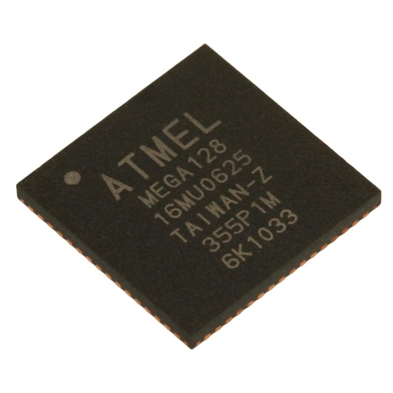
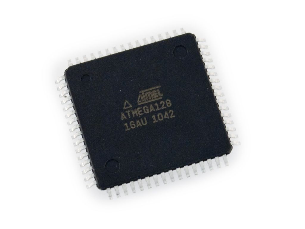
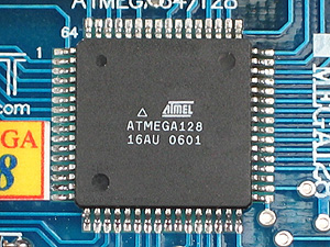
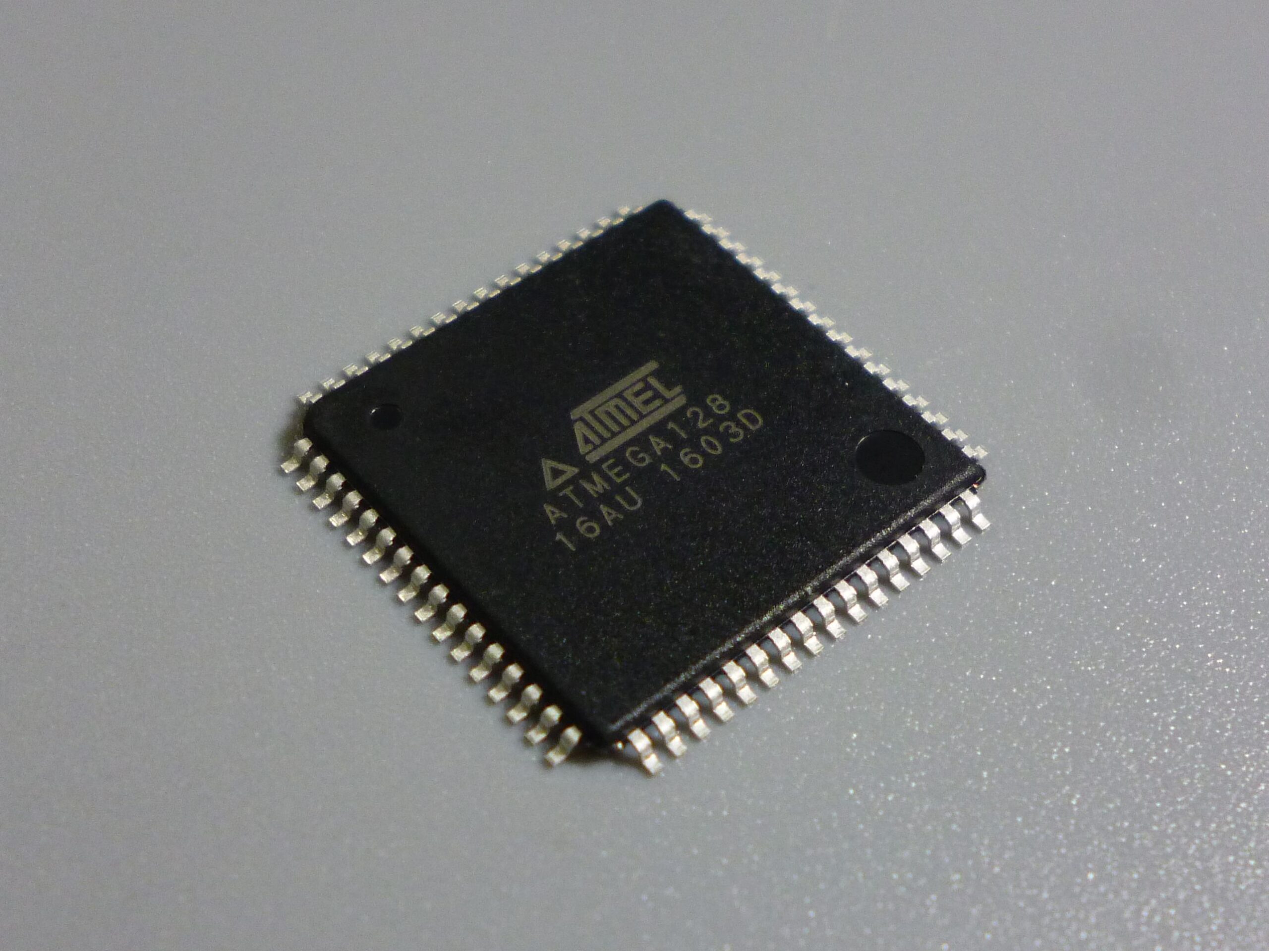
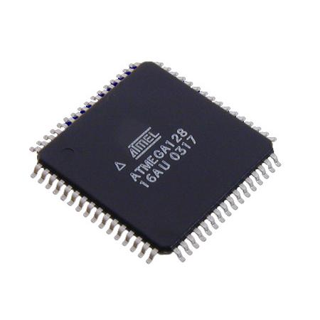
Break Microcontroller ATmega128 Heximal is a professional firmware recovery and analysis service designed for situations where embedded systems must be maintained, upgraded, or duplicated but original program assets are no longer available. The ATmega128 is a classic AVR microcontroller with a strong footprint in industrial automation, access control, instrumentation, consumer electronics, and educational platforms. Its balance of flash capacity, EEPROM storage, and peripheral flexibility has made it a long-term choice for embedded products that often remain in service far beyond their original development cycle.
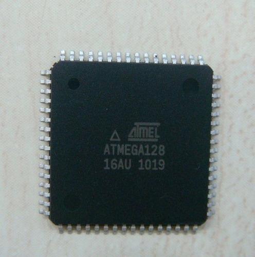
One of the defining features of the ATmega128 is its embedded architecture combining flash memory, EEPROM, SRAM, and multiple communication interfaces within a single secured device. To protect intellectual property, manufacturers frequently configure protective or locked security settings that restrict access to firmware, binary, or heximal files. While effective for production security, these mechanisms can become a barrier when systems require repair, migration, or controlled duplication. Our Break Microcontroller ATmega128 Heximal service addresses this gap by helping authorized clients retrieve embedded program data from protected or encrypted memory in a lawful and engineering-focused manner.
We can Break Microcontroller ATmega128 heximal, please view the Microcontroller Atmega128 features for your reference:
Features
· High-performance, Low-power AVR 8-bit Microcontroller
· Advanced RISC Architecture
– 133 Powerful Instructions – Most Single Clock Cycle Execution
– 32 x 8 General Purpose Working Registers + Peripheral Control Registers
– Fully Static Operation
– Up to 16 MIPS Throughput at 16 MHz
– On-chip 2-cycle Multiplier
Nonvolatile Program and Data Memories
– 128K Bytes of In-System Reprogrammable Flash
Endurance: 1,000 Write/Erase Cycles
– Optional Boot Code Section with Independent Lock Bits
In-System Programming by On-chip Boot Program
True Read-While-Write Operation
– 4K Bytes EEPROM
Endurance: 100,000 Write/Erase Cycles
– 4K Bytes Internal SRAM
– Up to 64K Bytes Optional External Memory Space
– Programming Lock for Software Security
– SPI Interface for In-System Programming
JTAG (IEEE std. 1149.1 Compliant) Interface
– Boundary-scan Capabilities According to the JTAG Standard
– Extensive On-chip Debug Support
– Programming of Flash, EEPROM, Fuses and Lock Bits through the JTAG Interface
Peripheral Features
– Two 8-bit Timer/Counters with Separate Prescalers and Compare Modes
– Two Expanded 16-bit Timer/Counters with Separate Prescaler, Compare Mode and Capture Mode
– Real Time Counter with Separate Oscillator
– Two 8-bit PWM Channels
– 6 PWM Channels with Programmable Resolution from 1 to 16 Bits
– 8-channel, 10-bit ADC
8 Single-ended Channels
7 Differential Channels
2 Differential Channels with Programmable Gain (1x, 10x, 200x)
– Byte-oriented 2-wire Serial Interface
– Dual Programmable Serial USARTs
– Master/Slave SPI Serial Interface
– Programmable Watchdog Timer with On-chip Oscillator
– On-chip Analog Comparator
Special Microcontroller Features
– Power-on Reset and Programmable Brown-out Detection
– Internal Calibrated RC Oscillator
– External and Internal Interrupt Sources
– Six Sleep Modes: Idle, ADC Noise Reduction, Power-save, Power-down, Standby and Extended Standby
– Software Selectable Clock Frequency
– ATmega103 Compatibility Mode Selected by a Fuse
– Global Pull-up Disable
I/O and Packages
– 53 Programmable I/O Lines
– 64-lead TQFP
Operating Voltages
– 2.7 – 5.5V (ATmega128L)
– 4.5 – 5.5V (ATmega128)
Speed Grades
– 0 – 8 MHz (ATmega128L)
– 0 – 16 MHz (ATmega128)
From a high-level perspective, recovering embedded firmware involves carefully attacking and breaking access restrictions without compromising data integrity. This may include controlled analysis of how flash and EEPROM protections are implemented, decoding memory layouts, and reconstructing consistent program archives from retrieved data. Rather than exposing technical methods, the emphasis is on outcome: restoring usable heximal, binary, or firmware files that can be validated, archived, and reused. Each project faces unique challenges, such as fragmented memory regions, secured readout logic, or aging silicon that requires delicate handling during analysis.
For end users, the value of this service is practical and measurable. Recovered firmware and source code equivalents enable legacy system support, spare-part reproduction, functional cloning, and compliant product upgrades without full redesign. This reduces downtime, lowers redevelopment costs, and preserves proven embedded solutions already deployed in the field. By offering a structured, discreet, and SEO-friendly service around ATmega128 firmware recovery, we support engineers, manufacturers, and maintenance teams who need reliable access to embedded memory data while respecting the complexity and security of modern microcontroller designs.
Break MCU ATmega128A Flash
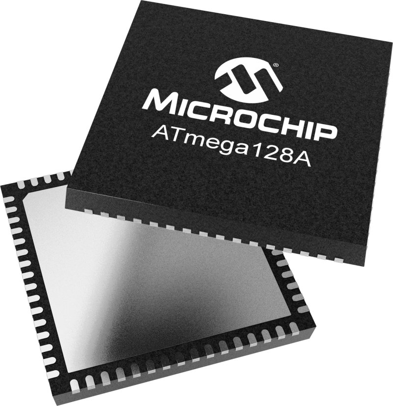
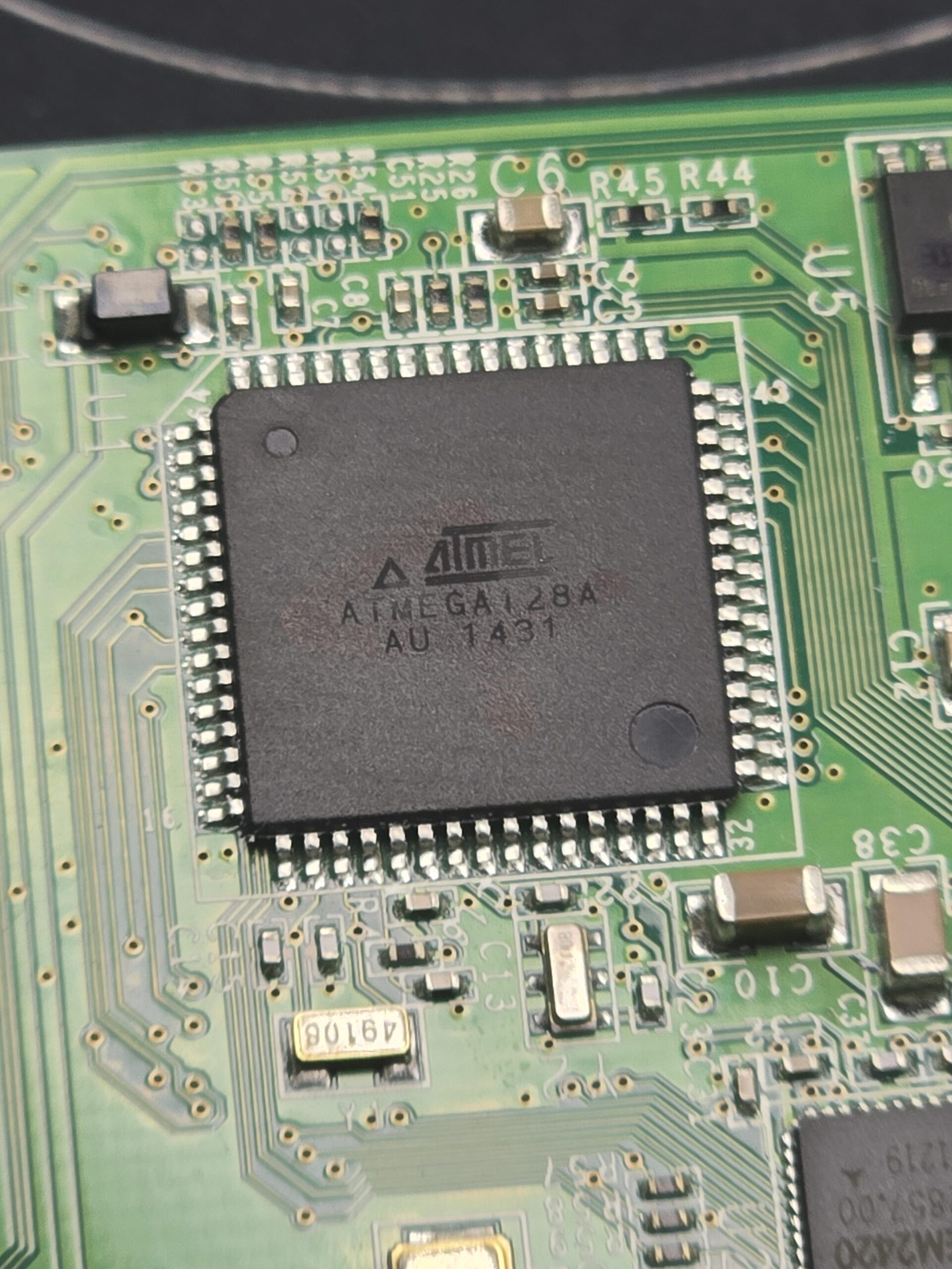
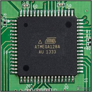
Break MCU ATmega128A Flash is a specialized service aimed at authorized clients who need to recover embedded firmware from legacy or secured AVR-based systems when original development assets are missing. The ATmega128A is a widely adopted 8-bit AVR microcontroller featuring large on-chip flash memory, EEPROM, SRAM, and a rich peripheral set. It has been deployed across industrial control, medical instruments, smart meters, laboratory equipment, consumer electronics, and educational platforms. Its long lifecycle and reliability make it common in products that must be maintained well beyond the original development phase.
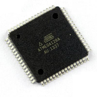
The ATmega128A stands out for its 128 KB flash, flexible EEPROM, multiple communication interfaces, and efficient low-power embedded architecture. To protect intellectual property, many manufacturers enable protective, protected, locked, or encrypted security configurations over the flash and memory regions. While these mechanisms secure firmware and source code during production, they can become obstacles when systems need to be refurbished, migrated, or duplicated. Our Break MCU ATmega128A Flash service focuses on helping clients legally attack and break these access barriers to retrieve binary or heximal program files in a controlled and professional manner.
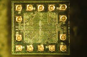
We can Break MCU Atmega128a Flash, please view the MCU Atmega128a features below for your reference:
Features
· High-performance, Low-power AVR 8-bit MCU
· Advanced RISC Architecture
– 133 Powerful Instructions – Most Single Clock Cycle Execution
– 32 x 8 General Purpose Working Registers + Peripheral Control Registers
– Fully Static Operation
– Up to 16 MIPS Throughput at 16 MHz
– On-chip 2-cycle Multiplier
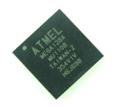
High Endurance Non-volatile Memory segments
– 128K Bytes of In-System Self-programmable Flash program memory
– 4K Bytes EEPROM
– 4K Bytes Internal SRAM
– Write/Erase cycles: 10,000 Flash/100,000 EEPROM
– Data retention: 20 years at 85°C/100 years at 25°C(1)
– Optional Boot Code Section with Independent Lock Bits
In-System Programming by On-chip Boot Program
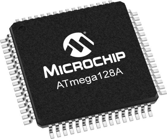
True Read-While-Write Operation to facilitate MCU Cracking
– Up to 64K Bytes Optional External Memory Space
– Programming Lock for Software Security
– SPI Interface for In-System Programming
JTAG (IEEE std. 1149.1 Compliant) Interface
– Boundary-scan Capabilities According to the JTAG Standard
– Extensive On-chip Debug Support
– Programming of Flash, EEPROM, Fuses and Lock Bits through the JTAG Interface
Peripheral Features
– Two 8-bit Timer/Counters with Separate Prescalers and Compare Modes
– Two Expanded 16-bit Timer/Counters with Separate Prescaler, Compare Mode and
Capture Mode
– Real Time Counter with Separate Oscillator
– Two 8-bit PWM Channels
– 6 PWM Channels with Programmable Resolution from 2 to 16 Bits
– Output Compare Modulator
– 8-channel, 10-bit ADC
8 Single-ended Channels
7 Differential Channels
2 Differential Channels with Programmable Gain at 1x, 10x, or 200x
– Byte-oriented Two-wire Serial Interface
– Dual Programmable Serial USARTs
– Master/Slave SPI Serial Interface
– Programmable Watchdog Timer with On-chip Oscillator
– On-chip Analog Comparator
Special MCU Features
– Power-on Reset and Programmable Brown-out Detection
– Internal Calibrated RC Oscillator
– External and Internal Interrupt Sources
– Six Sleep Modes: Idle, ADC Noise Reduction, Power-save, Power-down, Standby, and Extended Standby
– Software Selectable Clock Frequency
– ATmega103 Compatibility Mode Selected by a Fuse
– Global Pull-up Disable
I/O and Packages
– 53 Programmable I/O Lines
– 64-lead TQFP and 64-pad QFN/MLF
At a conceptual level, firmware recovery from a secured MCU involves analyzing how protection is implemented across flash, EEPROM, and internal memory. Challenges may include read-protected blocks, fragmented data archives, or embedded verification logic that prevents standard readout. Rather than relying on a single approach, our workflow may combine decoding, controlled decapsulation concepts, and signal-level analysis to retrieve consistent firmware data. The objective is not simply to hack the device, but to restore usable firmware archives that can be validated, cloned, or duplicated for engineering continuity.
For end users, the benefits are substantial. Recovered firmware, binary, or source code equivalents enable long-term maintenance, spare-part production, regulatory requalification, and smooth product upgrades without full redesign. This reduces cost, minimizes downtime, and preserves investment in proven embedded platforms. By offering a discreet, SEO-friendly, and industry-focused service model, we support manufacturers, repair centers, and system integrators who depend on secured embedded controllers, ensuring that valuable ATmega128A-based systems remain operational and sustainable for years to come.
Break IC MC9S12XDG128 Heximal
Break IC MC9S12XDG128 Heximal is a professional recovery and analysis service designed for organizations that must legally regain access to embedded firmware when original source code, documentation, or development partners are no longer available. The MC9S12XDG128 is a high-performance 16-bit microcontroller from the HCS12X family, widely recognized for its robust flash memory, EEPROM resources, and advanced embedded security features. It has been extensively deployed in automotive electronics, industrial automation, energy management systems, and mission-critical control modules where long product life cycles are common.
We can Break IC MC9S12XDG128 Heximal, please view below IC MC9S12XDG128 features for your reference:
Introduction
Targeted at automotive multiplexing applications, the MC9S12XD Family will deliver 32-bit performance with all the advantages and efficiencies of a 16-bit MCU. The S12X is designed to retain the low cost, low power consumption, excellent EMC performance and code-size efficiency advantages enjoyed by users of Freescale’s previous 16-bit MC9S12 MCU family.
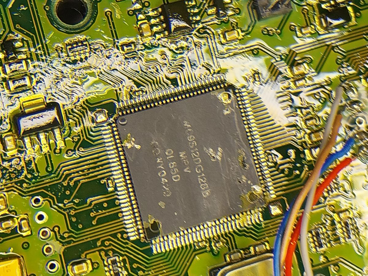
Based around an enhanced S12 core, the MC9S12XD Family will deliver two to five times the performance of a 25 MHz S12 whilst retaining a high degree of pin and code compatibility with the original S12D – family.
This microcontroller integrates on-chip flash, EEPROM, RAM, and a rich set of peripherals, making it suitable for complex embedded applications that demand reliability and deterministic performance. In many production environments, firmware, binary, or heximal program files are stored in protected, locked, or encrypted memory regions to secure intellectual property. Over time, these protective mechanisms can become a barrier when firmware archives are lost, hardware suppliers change, or systems require refurbishment. Our service focuses on helping authorized clients attack and break access restrictions in a controlled manner to retrieve secured firmware, memory data, or program files without exposing confidential technical details.
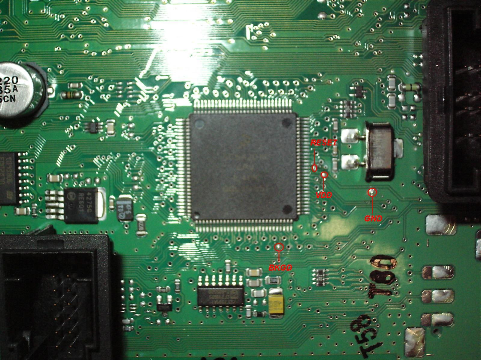
From a conceptual perspective, working with a secured MC9S12XDG128 involves understanding how embedded protection schemes interact with flash and EEPROM memory. Challenges may include locked boot sectors, encrypted firmware blocks, or fragmented archive data that cannot be accessed through standard programming tools. Each project requires careful analysis to decode and retrieve usable heximal or binary output while maintaining data consistency. Rather than simply copying memory, our goal is to restore structured firmware archives that can be used for validation, migration, or controlled duplication in a professional engineering environment.
The MC9S12XD Family features the performance boosting XGATE co-processor. The XGATE, which is programmable in “C” language, has an instruction set which is optimized for data movement, logic and bit manipulation instructions. It runs at twice the bus frequency of the S12X and off-loads the CPU by providing high speed data transfer (and data processing) between any peripheral module, RAM and I/O ports before Break IC. This is particularly useful in applications such as automotive gateways where there are multiple busses carrying heavy data traffic which would otherwise exert a heavy interrupt/processing load on the CPU.
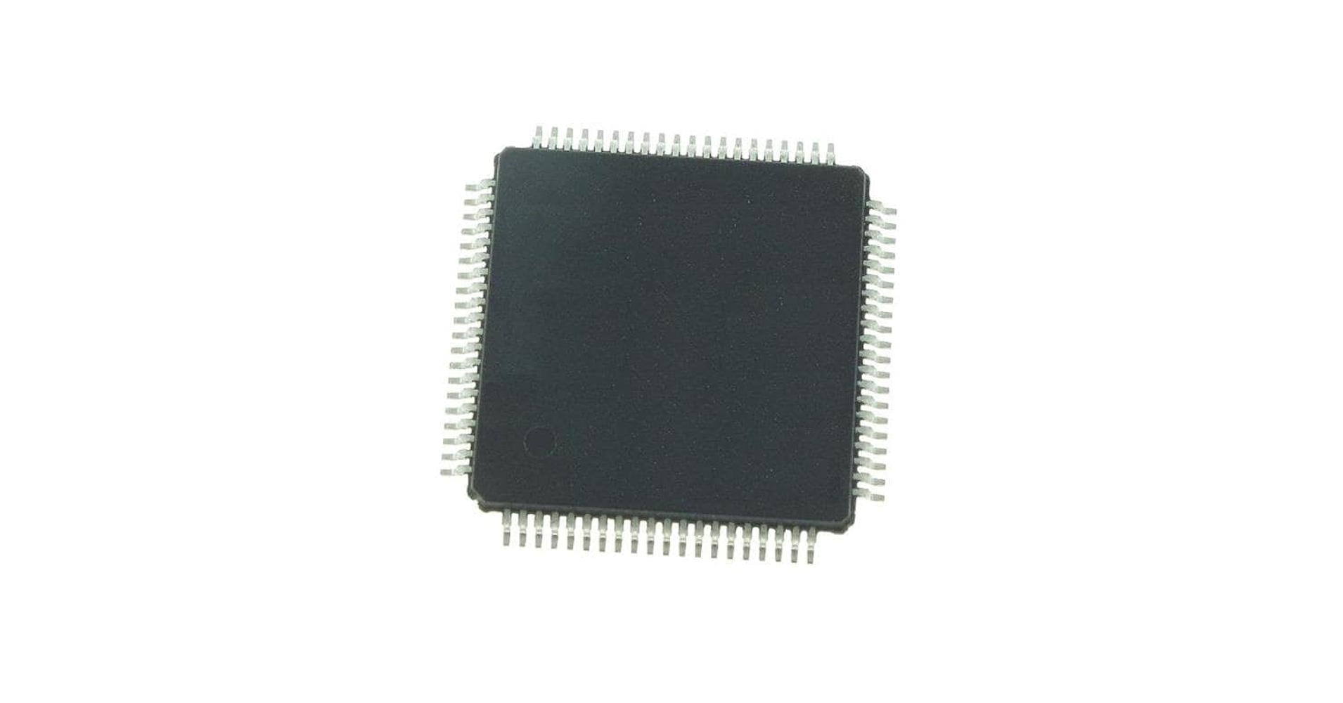
The MC9S12XD Family will feature an enhanced MSCAN module which, when used in conjunction with XGATE, delivers FullCAN performance with virtually unlimited number of mailboxes and retains backwards compatibility with the MSCAN module featured on previous S12 products.
Memory options will range from 64 Kbytes to 512 Kbytes of Freescale’s industry-leading, full automotive spec SG-Flash with additional integrated EEPROM.
In addition to the rich S12 peripheral set, the MC9S12XD Family will feature more RAM, extra A/D channels, new timer features and additional LIN-compatible SCI ports compared with the original S12 D Family. The MC9S12XD Family also features a new flexible interrupt handler which allows multilevel nested interrupts.
The MC9S12XD Family has full 16-bit data paths throughout. The non-multiplexed expanded bus interface available on the 144-pin versions allows an easy interface to external memories. The inclusion of a PLL circuit allows power consumption and performance to be adjusted to suit operational requirements. System power consumption is further improved with the new “fast exit from STOP mode” feature and an ultra low power wakeup timer. In addition to the I/O ports available in each module, up to 25 further I/O ports are available with interrupt capability allowing wakeup from STOP or WAIT mode. The MC9S12XD Family will be available in 144-pin LQFP (with optional external bus), 112-pin, and 80-pin options.
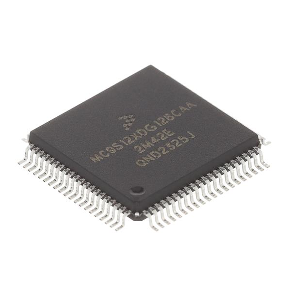
The benefits of the Break IC MC9S12XDG128 Heximal service are clear for end users facing operational risk or product obsolescence. Recovered firmware and source code equivalents allow companies to clone or duplicate legacy controllers, support after-sales maintenance, or transition designs to new platforms without full redevelopment. This reduces downtime, lowers engineering cost, and protects long-term investments in embedded systems. By offering a secure, discreet, and SEO-focused service model, we support industries that rely on protected microcontrollers while aligning technical recovery with real business and lifecycle requirements.
Break AVR ATmega64A Binary
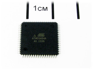
Break AVR ATmega64A Binary is a specialized engineering service designed to support manufacturers, system integrators, and maintenance teams that must legally regain access to embedded firmware when original development resources are unavailable. The AVR ATmega64A is a widely deployed 8-bit microcontroller known for its balanced performance, integrated flash and EEPROM memory, and flexible peripheral set. It is commonly used in industrial controllers, automation equipment, medical devices, smart instruments, and long-life consumer electronics.
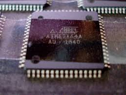
In many of these products, the firmware binary or heximal program becomes a critical asset over time, especially when devices remain operational long after the original supplier or source code archive is lost.
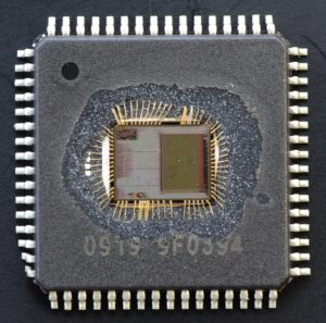
We can Break AVR ATMEGA64A Binary, please view below AVR ATMEGA64A features for your reference:
The ATmega64A features on-chip flash, EEPROM, and SRAM, combined with multiple communication interfaces and low-power operation, making it ideal for embedded systems that require stability and long-term availability. To protect intellectual property, vendors often enable protected, locked, or encrypted security configurations that restrict access to firmware, source code, and internal memory data. While these protective mechanisms are effective for IP control, they can create serious obstacles during product refurbishment, failure analysis, migration, or compliance verification. Our service focuses on helping authorized clients attack, break, decode, or retrieve essential program files and embedded firmware in a controlled and professional manner, without disclosing sensitive technical details.
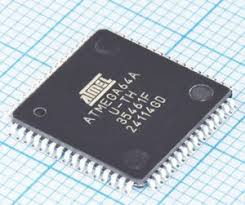
· High-performance, Low-power AVR® 8-bit Microcontroller
· Advanced RISC Architecture
– 130 Powerful Instructions – Most Single Clock Cycle Execution
– 32 x 8 General Purpose Working Registers + Peripheral Control Registers
– Fully Static Operation
– Up to 16 MIPS Throughput at 16 MHz
– On-chip 2-cycle Multiplier
High Endurance Non-volatile Memory segments
– 64K Bytes of In-System Reprogrammable Flash program memory
– 2K Bytes EEPROM
– 4K Bytes Internal SRAM
– Write/Erase Cycles: 10,000 Flash/100,000 EEPROM
– Data retention: 20 years at 85°C/100 years at 25°C(1)
– Optional Boot Code Section with Independent Lock Bits
· In-System Programming by On-chip Boot Program
· True Read-While-Write Operation
– Up to 64K Bytes Optional External Memory Space
– Programming Lock for Software Security
– SPI Interface for In-System Programming
JTAG (IEEE std. 1149.1 Compliant) Interface
– Boundary-scan Capabilities According to the JTAG Standard
– Extensive On-chip Debug Support
– Programming of Flash, EEPROM, Fuses, and Lock Bits through the JTAG Interface
Peripheral Features
– Two 8-bit Timer/Counters with Separate Prescalers and Compare Modes
– Two Expanded 16-bit Timer/Counters with Separate Prescaler, Compare Mode, and Capture Mode
– Real Time Counter with Separate Oscillator
– Two 8-bit PWM Channels
– 6 PWM Channels with Programmable Resolution from 1 to 16 Bits
– 8-channel, 10-bit ADC
· 8 Single-ended Channels
· 7 Differential Channels
· 2 Differential Channels with Programmable Gain (1x, 10x, 200x)
– Byte-oriented Two-wire Serial Interface
– Dual Programmable Serial USARTs
– Master/Slave SPI Serial Interface
– Programmable Watchdog Timer with On-chip Oscillator
– On-chip Analog Comparator
Special Microcontroller Features
– Power-on Reset and Programmable Brown-out Detection
– Internal Calibrated RC Oscillator
– External and Internal Interrupt Sources when Break AVR
– Six Sleep Modes: Idle, ADC Noise Reduction, Power-save, Power-down, Standby and Extended Standby
– Software Selectable Clock Frequency
– ATmega103 Compatibility Mode Selected by a Fuse
– Global Pull-up Disable I/O and Packages
– 53 Programmable I/O Lines
– 64-lead TQFP and 64-pad QFN/MLF Operating Voltages
– 2.7 – 5.5V for ATmega64A Speed Grades
From a high-level perspective, recovering a secured AVR ATmega64A binary requires deep understanding of the MCU architecture, memory organization, and protection logic. Challenges often include locked flash regions, secured EEPROM blocks, and fragmented archive data that cannot be accessed through standard programming interfaces. Each case is different, and the difficulty depends on firmware size, security configuration, and device condition. Our engineers apply advanced analysis and controlled recovery workflows to clone or duplicate the required firmware, binary, or heximal file while preserving data integrity. The goal is not simply to copy memory, but to restore usable program archives that can support engineering, validation, or controlled reproduction.
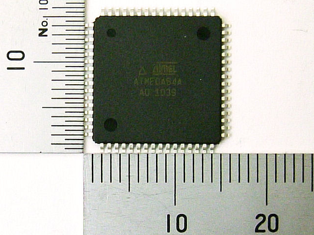
The business value of our Break AVR ATmega64A Binary service lies in risk reduction and lifecycle continuity. End users benefit by avoiding costly redesigns, minimizing downtime, and extending the usable life of embedded products. Recovered firmware and memory data can be used for backup, migration to new hardware, compatibility testing, or regulated documentation. By offering a secure, discreet, and SEO-focused service model, we support industries that rely on embedded systems while respecting confidentiality and commercial requirements. Our role is to provide a reliable technical bridge between protected microcontrollers and real-world operational needs.
Break IC ATmega169P Code
The calibrated internal RC Oscillator provides a fixed 8.0 MHz clock. The frequency is nominal value at 3V and 25°C. If 8 MHz frequency exceeds the specification of the device (depends on VCC), the CKDIV8 Fuse must be programmed in order to divide the internal frequency by 8 during start-up to facilitate Break IC ATmega169P Code.
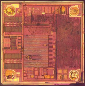
Break IC ATmega169P Code
The device is shipped with the CKDIV8 Fuse programmed. See “System Clock Prescaler” on page 29. for more details. This clock may be selected as the system clock by programming the CKSEL Fuses as shown in Table 8. If selected, it will operate with no external components. During reset, hardware loads the calibration byte into the OSCCAL Register and thereby automatically calibrates the RC Oscillator.
At 3V and 25°C, this calibration gives a frequency within ± 10% of the nominal frequency. Using calibration methods as described in application notes available at www.atmel.com/avr it is possible to achieve ± 2% accuracy at any given VCC and Temperature. When this Oscillator is used as the IC clock, the Watchdog Oscillator will still be used for the Watchdog Timer and for the Reset Time-out.
For more information on the pre-programmed calibration value, see the section “Calibration Byte” on page 269. When this Oscillator is selected, start-up times are determined by the SUT Fuses as shown in Table 9. Selecting internal RC Oscillator allows the XTAL1/TOSC1 and XTAL2/TOSC2 pins to be used as timer oscillator pins.
Writing the calibration byte to this address will trim the internal Oscillator to remove process variations from the Oscillator frequency. This is done automatically during IC Reset. When OSCCAL is zero, the lowest available frequency is chosen in the process of Break IC ATmega169P Code. Writing nonzero values to this register will increase the frequency of the internal Oscillator.
Writing 0x7F to the register gives the highest available frequency. The calibrated Oscillator is used to time EEPROM and Flash access. If EEPROM or Flash is written, do not calibrate to more than 10% above the nominal frequency. Otherwise, the EEPROM or Flash write may fail. Note that the Oscillator is intended for calibration to 8.0 MHz. Tuning to other values is not guaranteed, as indicated in Table 10.
When applying an external clock, it is required to avoid sudden changes in the applied clock frequency to ensure stable operation of the MCU. A variation in frequency of more than 2% from one clock cycle to the next can lead to unpredictable behavior. It is required to ensure that the MCU is kept in Reset during such changes in the clock frequency.
Note that the System Clock Prescaler can be used to implement run-time changes of the internal clock frequency while still ensuring stable operation. Refer to “System Clock Prescaler” on page 29 for details. When the CKOUT Fuse is programmed, the system Clock will be output on CLKO. This mode is suitable when IC clock is used to drive other circuits on the system.
The clock will be output also during reset and the normal operation of I/O pin will be overridden when the fuse is programmed. Any clock source, including internal RC Oscillator, can be selected when CLKO serves as clock output. If the System Clock Prescaler is used, it is the divided system clock that is output when the CKOUT Fuse is programmed.
Break Chip PIC16F59 Eeprom
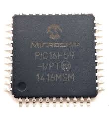
Modern industrial systems rely heavily on stable low-power microcontrollers, and the Microchip PIC16F59 remains a popular choice in manufacturing, appliance control, compact automation modules, and a wide range of embedded designs. As equipment ages, owners often face difficulties accessing the eeprom, flash, and internal memory due to protected, locked, or encrypted configurations. Our high-end service, introduced under the subject Break Chip PIC16F59 EEPROM, is designed to help legitimate clients safely retrieve operational data, program logic, and legacy firmware without exposing any attack techniques.
The high performance of the PIC16F5X family can be attributed to a number of architectural features commonly found in RISC microprocessors to Break Chip PIC16F59 Eeprom. To begin with, the PIC16F5X uses a Harvard architecture in which program and data are accessed on separate buses.
Industry Use Cases & Unique Features of PIC16F59
The PIC16F59 is widely used because of its flexible architecture, low power consumption, and stable embedded design. You will find it in:
- Household electronic controllers
- Industrial signal modules and measurement devices
- Educational hardware, training boards, and simple robotics
- Automotive auxiliary electronics
- Consumer and semi-industrial automation tools
Its internal 12-bit core, versatile I/O structure, and reliable eeprom storage make it a long-term favorite among OEMs. Many manufacturers build custom logic inside this device, making the stored binary or heximal archive extremely valuable to business continuity.
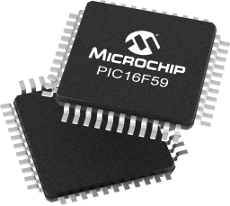
This improves bandwidth over traditional von Neumann architecture where program and data are fetched on the same bus. Separating program and data memory further allows instructions to be sized differently than the 8-bit wide data word. Instruction opcodes are 12-bits wide, making it possible to have all single-word instructions. A 12-bit wide program memory access bus fetches a 12-bit instruction in a single cycle.
A two-stage pipeline overlaps fetch and execution of instructions. Consequently, all instructions (33) execute in a single cycle except for program branches. The PIC16F54 addresses 512 x 12 of program memory, the PIC16F57 and PIC16F59 addresses 2048 x 12 of program memory. All program memory is internal.
The PIC16F5X can directly or indirectly address its register files and data memory. All Special Function Registers (SFR), including the program counter, are mapped in the data memory. The PIC16F5X has a highly orthogonal (symmetrical) instruction set that makes it possible to carry out any operation on any register using any Addressing mode when Break Chip PIC16F59 Eeprom. This symmetrical nature and lack of ‘special optimal situations’ make programming with the PIC16F5X simple, yet efficient. In addition, the learning curve is reduced significantly.
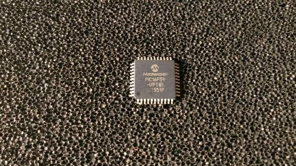
The PIC16F5X device contains an 8-bit ALU and working register. The ALU is a general purpose arithmetic unit. It performs arithmetic and Boolean functions between data in the working register and any register file.
What Our Service Provides
Our service assists authorized device owners who need to break through inaccessible flash or eeprom regions due to forgotten revisions, discontinued suppliers, or lost source code. We support scenarios where systems must continue running for many years, but the original file or firmware is no longer obtainable.
We help legitimate clients:
- Retrieve the internal program and operational data
- Clone or duplicate their existing unit for maintenance or redesign
- Rebuild missing archive records for long-term service
- Recover critical logic damaged by aging components
Although some devices require inspection or controlled decapsulation, we do not disclose any internal processes. The goal is always to return a verified, functional binary or heximal image of your own property.
The ALU is 8-bits wide and capable of addition, subtraction, shift and logical operations. Unless otherwise mentioned, arithmetic operations are two’s complement in nature. In two-operand instructions, typically one operand is the W (working) register. The other operand is either a file register or an immediate constant. In single operand instructions, the operand is either the W register or a file register.
General High-Level Recovery Concept (Non-technical & Safe)
The process begins with a feasibility assessment based on device condition, level of secured configuration, and memory integrity. Some units require physical stabilization or deeper evaluation, while others can be processed through standardized extraction workflows designed to respect IP ownership, legal compliance, and data confidentiality.
Our team does not “teach” customers how to hack, decode, or attack the security. Instead, we perform all procedures internally and return only the final, usable file.
Purpose & Benefits for End Users
Clients choose this service because it helps them:
- Keep old machinery running without redesign
- Preserve unique source code and calibration data
- Extend the life cycle of products reliant on PIC16F59
- Avoid costly downtime caused by lost or inaccessible firmware
- Ensure a secure, company-controlled archive for future engineering
By providing a complete and validated memory image, we enable stable maintenance, redesign, or modernization.
Typical Challenges We Encounter
Recovery of PIC16F59 may involve:
- Heavily protected or embedded firmware regions
- Partial memory decay or corruption
- Environmental wear or physical damage
- Complex security configurations depending on revision
Despite these difficulties, our methodical workflow and advanced evaluation tools help ensure high success rates under legally authorized conditions.
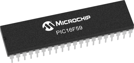
The W register is an 8-bit working register used for ALU operations. It is not an addressable register. Depending on the instruction executed, the ALU may affect the values of the Carry (C), Digit Carry (DC) and Zero (Z) bits in the STATUS Register to Extract IC code. The C and DC bits operate as a borrow and digit borrow out bit, respectively, in subtraction. See the SUBWF and ADDWF instructions for examples.
A simplified block diagram is shown in Figure 2-1 with the corresponding device pins described in Table 2-1 (for PIC16F54), Table 2-2 (for PIC16F57) and Table 2-3 (for PIC16F59).
Break Microcontroller PIC16F628A Content
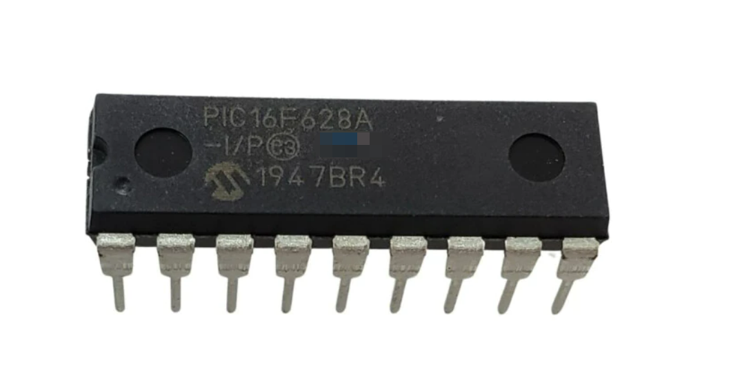
In many long-running products, industrial tools, and legacy control modules, the Microchip PIC16F628A remains a highly trusted and widely deployed microcontroller. Its balance of cost, performance, and stable embedded design makes it a backbone component across manufacturing equipment, consumer devices, smart access systems, and compact automation solutions. When access to its flash, EEPROM, or internal memory becomes restricted due to protective, locked, or encrypted settings, equipment owners may struggle to maintain or revive their production assets. Our authorized recovery service, introduced under the subject Break Microcontroller PIC16F628A Content, is specifically created to help legitimate customers regain access to their own data, program configuration, and operational firmware without disclosing technical attack methods.
Industry Use Cases of PIC16F628A
The PIC16F628A is extensively adopted in:
- Compact automation controllers and industrial timers
- Entry-level motor drivers and sensor control modules
- Communication interface boards and remote monitors
- Consumer appliances and low-power handheld devices
Because these applications store calibrated parameters, system logic, or customer-specific source code, preserving or retrieving the internal archive becomes critical whenever the hardware needs repair, replacement, or upscaling.
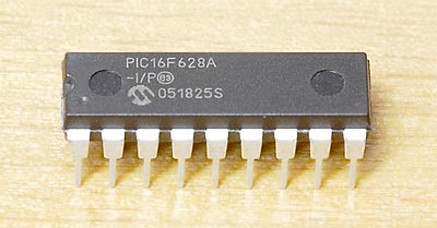
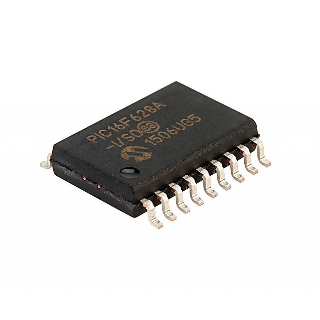
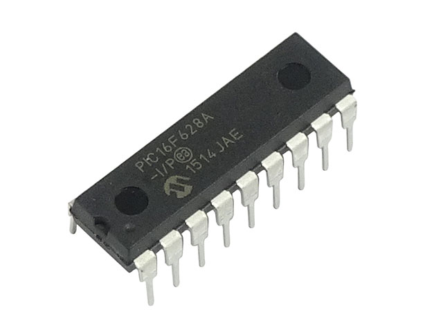
We can break Microcontroller PIC16F628A Content, please view the Microcontroller PIC16F628A features for your reference:
GENERAL DESCRIPTION
The PIC16F627A/628A/648A are 18-Pin FLASH-based members of the versatile PIC16CXX family low cost, high performance, CMOS, fully-static, 8-bit microcontroller.
All PICmicro® microcontrollers employ an advanced RISC architecture. The PIC16F627A/628A/648A have enhanced core features, eight-level deep stack, and multiple internal and external interrupt sources. The separate instruction and data buses of the Harvard architecture allow a 14-bit wide instruction word with the separate 8-bit wide data.
The two-stage instruction pipeline allows all instructions to execute in a single-cycle, except for program branches (which require two cycles). A total of 35 instructions (reduced instruction set) are available, complemented by a large register set.
Our service focuses on helping authorized owners retrieve, clone, or duplicate the binary or heximal image stored in the PIC16F628A’s flash and EEPROM regions. Many units are shipped with protected or secured settings that prevent unauthorized copying; however, legitimate companies may still need to break barriers caused by forgotten revision histories, unavailable designers, supplier bankruptcy, or aging hardware.
We support clients by generating a verified file containing the extracted program and operational data, ensuring that future repairs or redesigns remain possible. All engagements emphasize confidentiality, legal compliance, and IP ownership verification.
General High-Level Concept (Non-Technical & Non-Actionable)
A typical recovery evaluation looks at the device condition, the level of encrypted or locked configuration, and possible integrity issues within the embedded memory. In some cases, physical analysis may be required, such as chip inspection or authorized decapsulation assessments, though details of any internal processes are never disclosed.
The objective is not to teach customers how to hack, decode, or attack a device, but rather to deliver a complete, usable archive that restores their ability to maintain, continue, or evolve their own systems.
PIC16F628A microcontrollers typically achieve a 2:1 code compression and a 4:1 speed improvement over other 8-bit microcontrollers in their class. PIC16F627A/628A/648A devices have integrated features to reduce external components, thus reducing system cost, enhancing system reliability and reducing power consumption.
The PIC16F628A has 8 oscillator configurations. The single-pin RC oscillator provides a low cost solution. The LP oscillator minimizes power consumption, XT is a standard crystal, and INTOSC is a self-contained precision two-speed internal oscillator to read MCU. The family HS is for High-Speed crystals. The EC mode is for an external clock source.
Clients turn to our service for several legitimate reasons:
- Restoring access to lost or outdated firmware
- Migrating old product lines to new hardware platforms
- Preparing backup binary archives for compliance or safety audits
- Rebuilding operational settings when the original design house is unavailable
- Maintaining machines that must stay functional for many more years
With a validated memory file, businesses avoid production downtime, eliminate guesswork, and continue improving their systems with confidence.
Challenges We May Encounter
Projects involving PIC16F628A often involve obstacles such as:
- Deeply protected configuration bits
- Possible memory wear and partial corruption
- Device variants with different internal layouts
- Environmental damage or aging affecting access reliability
Nonetheless, our team provides clear feasibility evaluations, transparent expectations, and controlled, professional workflow throughout the entire recovery cycle.
 Posted in Break IC |
  Tags: break microcontroller source binary, break microcontroller source content, break microcontroller source data, break microcontroller source file, break microcontroller source flash, break microcontroller source hex, break microcontroller source software, zerwać mcu bin, zerwać mcu code, zerwać mcu data, zerwać mcu eeprom, zerwać mcu file, zerwać mcu firmware, zerwać mcu hex, zerwać mcu memory, zerwać mcu program |
  Comments Closed
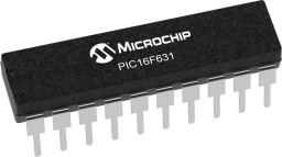
Break MCU PIC16F631 Flash
When a device depends on the Microchip PIC16F631 for control, timing, or sensor interfacing, loss of access to on-chip flash or EEPROM can stop equipment and erase critical calibration data. Our service, indexed as Break MCU PIC16F631 Flash, helps legitimate owners and authorized technicians open, readout, restore, and duplicate the embedded firmware/binary/heximal images stored in these controllers. We focus on safe, lawful recovery that returns usable program archives without revealing methods to crack, hack, or bypass protections.
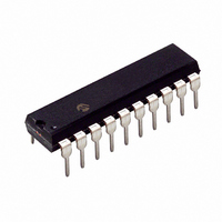
Clients commonly need us to restore corrupted files, copy firmware for authorized spares, clone settings for production, or duplicate configuration archives before servicing legacy systems. Devices using the PIC16F631 often contain small but vital pieces of source code, calibration tables and settings in flash or EEPROM — assets that, when protected, may be inaccessible without professional, authorized support.
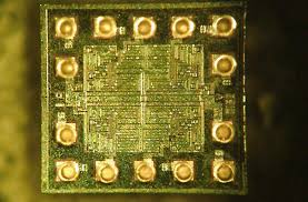
We can Break MCU PIC16F685 flash, please view the MCU PIC16F685 features for your reference:
High-Performance RISC CPU:
· Only 35 instructions to learn:
– All single-cycle instructions except branches
The PIC16F631’s compact footprint and mixed-signal capabilities make it a frequent choice across many industries:
- Consumer electronics and appliance controllers.
- Industrial sensors and simple automation modules.
- Instrumentation and small test equipment.
- Aftermarket automotive modules and hobbyist/legacy embedded systems.
Because these applications store operational data and program archives on the device, being able to recover a verified binary or heximal dump can be essential to restore service quickly.
· Operating speed:
– DC – 20 MHz oscillator/clock input
– DC – 200 ns instruction cycle
· Interrupt capability
· 8-level deep hardware stack
· Direct, Indirect and Relative Addressing modes
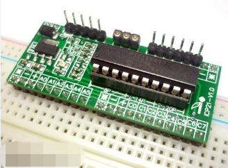
Special Microcontroller Features:
· Precision Internal Oscillator:
– Factory calibrated to ± 1%
– Software selectable frequency range of 8 MHz to 32 kHz
– Software tunable
– Two-Speed Start-up mode
– Crystal fail detect for critical applications
– Clock mode switching during operation for power savings
· Power-Saving Sleep mode
· Wide operating voltage range (2.0V-5.5V)
· Industrial and Extended Temperature range
· Power-on Reset (POR)
· Power-up Timer (PWRTE) and Oscillator Start-up Timer (OST)
· Brown-out Reset (BOR) with software control option and for MCU reading
· Enhanced low-current Watchdog Timer (WDT) with on-chip oscillator (software selectable nominal 268 seconds with full prescaler) with software enable
· Multiplexed Master Clear/Input pin
· Programmable code protection
· High Endurance Flash/EEPROM cell:
– 100,000 write Flash endurance
– 1,000,000 write EEPROM endurance
– Flash/Data EEPROM retention: > 40 years
· Enhanced USART module:
– Supports RS-485, RS-232 and LIN 2.0
– Auto-Baud Detect
– Auto-wake-up on Start bit
The PIC16F631 integrates modest program flash, EEPROM, and analog/digital peripherals in a tight package. Its memory layout concentrates configuration and calibration data in discrete regions, and many designs set protective or locked configurations to prevent unauthorized copying. Those features shape how a lawful recovery is scoped and the kinds of deliverables that best serve the end user.
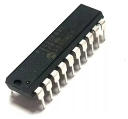
What we provide (high level, non-actionable)
Our engagements emphasize ethical, non-destructive recovery. Typical deliverables include validated binary/heximal dumps of flash and EEPROM where permitted, integrity and checksum reports, and high-level annotated summaries that help engineers interpret recovered program logic. We can assist clients to restore devices to operation using recovered files, prepare migration packages for replacement hardware, and advise on safe duplication and archival strategies. Importantly, we do not publish or provide step-by-step instructions to decrypt, unlock, or otherwise compromise manufacturer protections.
Conceptual approach and purpose
A responsible recovery project begins with verification of ownership and a feasibility assessment. The objective is to obtain a reliable memory archive and translate raw data into a usable representation for maintenance, testing, or authorized redevelopment. The primary purposes are to reduce downtime, secure previously inaccessible firmware, and enable legitimate copying or cloning for spares and production.
Benefits for the end user
Clients benefit from secure backups of embedded firmware and data, faster restoration of equipment, and the ability to duplicate or deploy authorized copies across installations. Recovered program archives reduce the need to rebuild software from scratch and protect investment in specialized hardware.
Challenges and limitations
Obstacles can include layered protective settings, partial memory corruption, variant device revisions, and proprietary integrity checks. Full source-level reconstruction is not always possible; often the practical outcome is a validated heximal or binary archive with assembly-level annotations. We communicate feasibility and likely outcomes before proceeding.
Legal & ethical safeguards
All projects require explicit authorization and operate under confidentiality agreements. Our mission is to help rightful owners recover, restore, and preserve their embedded systems for lawful, constructive purposes only.
If you need to Break MCU PIC16F631 Flash for authorized recovery, maintenance, or archival purposes, our experienced team provides confidential, professional support to retrieve and document your embedded program and data while protecting your IP and operational continuity.
Posted in Break IC |
Tags: break mcu encrypted bin, break mcu encrypted content, break mcu encrypted data, break mcu encrypted file, break mcu encrypted flash, break mcu encrypted hex, break mcu encrypted software, złamać mcu bin, złamać mcu code, złamać mcu data, złamać mcu eeprom, złamać mcu file, złamać mcu firmware, złamać mcu flash, złamać mcu hex, złamać mcu memory, złamać mcu program, złamać mcu software |
Comments Closed
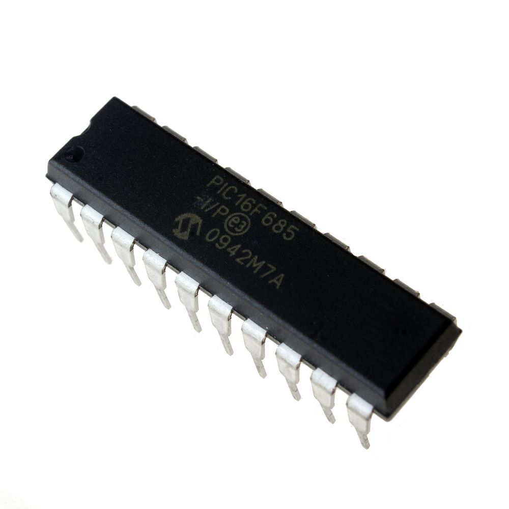
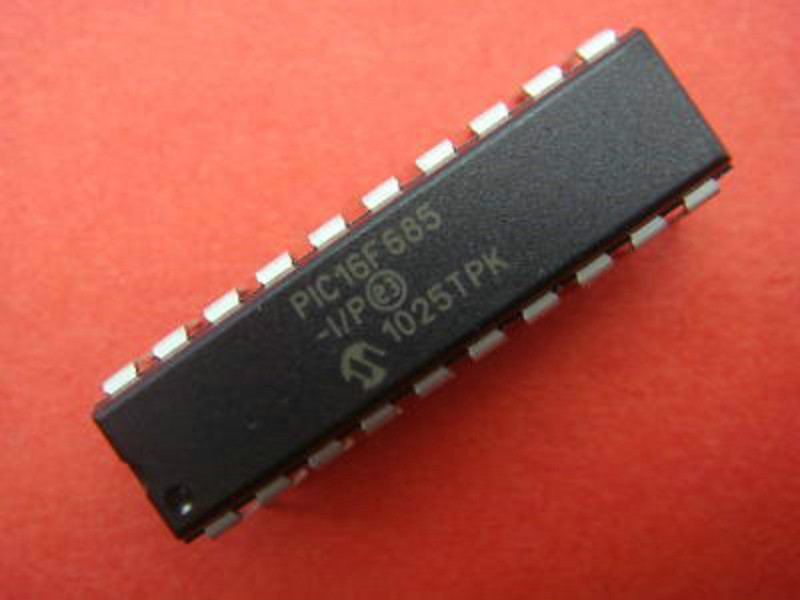
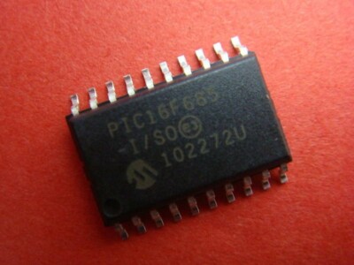
Break IC PIC16F685 Code
When an embedded system depends on the Microchip PIC16F685, losing access to its program or finding the device set to protected can halt operations and complicate maintenance. Our service, searchable under the keyword Break IC PIC16F685 Code, helps authorized owners and engineers open, readout, restore, and duplicate the firmware/binary/heximal contents of these microcontrollers. We deliver validated memory archives and high-level analysis while strictly avoiding publication of methods to illegally crack or hack protections.
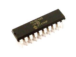
The need to copy, clone, or duplicate a PIC16F685’s program file arises in many legitimate scenarios: restoring corrupted flash or EEPROM after a failure, recovering crucial calibration data, preparing authorized spares, or migrating long-lived products to replacement hardware. In many cases the firmware is locked or secured by the original integrator; safely extracting a verified binary or heximal dump can be the fastest route to restore operation without redesign.
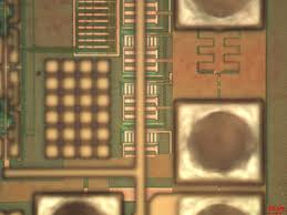
We can Break IC PIC16F685 Code, please view the Ic PIC16F685 features for your reference:
The PIC16F685 has a 13-bit program counter capable of addressing an 8K x 14 program memory space. Only the first 1K x 14 (0000h-03FFh) is physically implemented for the PIC16F631, the first 2K x 14 (0000h-07FFh) for the PIC16F677/PIC16F687, and the first 4K x 14 (0000h-0FFFh) for the PIC16F685/PIC16F689/ PIC16F690 when Break Ic. Accessing a location above these boundaries will cause a wraparound. The Reset vector is at 0000h and the interrupt vector is at 0004h.
The data memory (see Figures 2-6 through 2-8) is partitioned into four banks which contain the General Purpose Registers (GPR) and the Special Function Registers (SFR). The Special Function Registers are located in the first 32 locations of each bank. The CALL, RETURN RETFIE, RETLW.
General Purpose Registers, implemented as static RAM, are located in the last 96 locations of each Bank. Register locations F0h-FFh in Bank 1, 170h-17Fh in Bank 2 and 1F0h-1FFh in Bank 3 point to addresses 70h-7Fh in Bank 0. The actual number of General Purpose Resisters (GPR) in each Bank depends on the device. Details are shown in Figures 2-4 through 2-8.
All other RAM is unimplemented and returns ‘0’ when Reset Vector 0000h read. RP<1:0> of the STATUS register are the bank select bits:
The register file is organized as 128 x 8 in the PIC16F687 and 256 x 8 in the PIC16F685/PIC16F689/PIC16F690. Each register is accessed, either directly or indirectly, through the File Select Register (FSR) (see Section 2.4 “Indirect Addressing, INDF and FSR Registers”) by Break IC PIC16F685 Code.
SPECIAL FUNCTION REGISTERS
The Special Function Registers are registers used by the CPU and peripheral functions for controlling the desired operation of the device for MCU Reading (see Tables 2-1 through 2-4). These registers are static RAM.
The special registers can be classified into two sets: core and peripheral. The Special Function Registers associated with the “core” are described in this section. Registers related to the operation of peripheral features are described in the section of that peripheral feature.
The PIC16F685 is widely used where compact control and analog interfacing matter:
- Consumer electronics and appliance controllers.
- Industrial sensors and small automation modules.
- Instrumentation such as data loggers and test front-ends.
- Aftermarket automotive modules and hobbyist/legacy embedded systems.
Because these devices often store important configuration data and small program archives in on-chip memory, access to those files is frequently necessary for repair and continuity.
Unique features that affect recovery
This MCU combines flexible I/O, analog peripherals, and modest on-chip flash and EEPROM storage. Its architecture means that both program and calibration data may be tightly integrated, and many designs apply protective settings to prevent unauthorized copying. Those characteristics shape how recovery is approached and the kinds of deliverables that are most useful to end users.
What we provide (high-level, non-actionable)
Our engagements focus on ethical, non-destructive recovery outcomes. Typical services include: validated extraction of memory images (producing binary/heximal dumps), integrity checks and verification reports, and high-level disassembly summaries that help engineers interpret recovered program logic. We can assist clients in using recovered files to restore devices to operation or prepare migration packages for replacement hardware. We do not provide step-by-step instructions or tools intended to decrypt, bypass, or otherwise subvert manufacturer or integrator-applied protections.
General idea (conceptual)
A responsible recovery project begins with ownership verification and a feasibility assessment. Engineers then pursue conservative, evidence-based techniques to obtain a reliable archive of the device’s memory and to validate its integrity. The aim is to return a usable program image that enables authorized copying, duplication, or rebuilding while preserving device health and intellectual property.
Benefits and likely outcomes
Clients who use this service gain secure backups of previously inaccessible firmware and data, reduced downtime through faster restoration, and the ability to clone or duplicate devices for approved spares provisioning. Recovered binary or heximal archives support testing, compliance checks, and migration without starting from scratch.
Challenges and limitations
Recovery may be hindered by layered protections, partial data corruption, variant hardware revisions, or proprietary integrity checks. Full source-code reconstruction is not always possible; often the realistic deliverable is a validated firmware image with assembly-level annotations.
Ethics and authorization
We require proof of ownership or explicit authorization for all projects and operate under strict confidentiality agreements. Our mission is to help rightful owners unlock, restore, and preserve their embedded systems for lawful, constructive purposes only.
If you need to Break IC PIC16F685 Code for authorized recovery, maintenance, or archival purposes, our team provides confidential, professional support to retrieve and document your embedded firmware and data while protecting your IP and operational continuity.
Posted in Break IC |
Tags: odnaleźć układ scalony bin, odnaleźć układ scalony code, odnaleźć układ scalony data, odnaleźć układ scalony eeprom, odnaleźć układ scalony file, odnaleźć układ scalony firmware, odnaleźć układ scalony hex, odnaleźć układ scalony memory, odnaleźć układ scalony program |
Comments Closed