Archive for the ‘Recover MCU’ Category
 Reverse MCU ATmega461PV Binary
 April 30th, 2010 |
  Author:
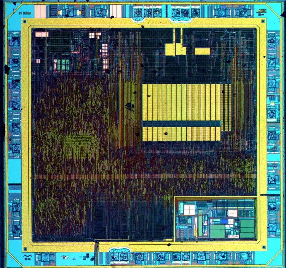
 Reverse MCU ATmega461PV and readout microcontroller atmega461pv secured Binary, crack mcu protective system and using focus ion beam to cut off the security fuse bit;
The interconnection between Master and Slave CPUs with SPI is shown in Figure 80. The system consists of two shift Registers, and a Master clock generator. Th e SPI Master initiates the communication cycle when pulling low the Slave Select SS pin of the desired Slave.
Master and Slave prepare the data to be sent in their respective shift Registers, and the Master generates the required clock pulses on the SCK line to interchange data if break atmega64pa MCU binary.
Data is always shifted from Master to Slave on the Master Out – Slave In, MOSI, line, and from Slave to Master on the Master In – Slave Out, MISO, line. After each data packet, the Master will synchronize the Slave by pulling high the Slave Select, SS, line.
When configured as a Master, the SPI interface has no automatic control of the SS line. This must be handled by user software before communication can start. When this is done, writing a byte to the SPI Data Register starts the SPI clock generator, and the hardware shifts the eight bits into the Slave. After shifting one byte, the SPI clock generator stops, setting the end of Transmission Flag (SPIF) after break atmega128a MCU firmware.
If the SPI Interrupt Enable bit (SPIE) in the SPCR Register is set, an interrupt is requested. The Master may continue to shift the next byte by writing it into SPDR, or signal the end of packet by pulling high the Slave Select, SS line. The last incoming byte will be kept in the Buffer Register for later use. When configured as a Slave, the SPI interface will remain sleeping with MISO tri-stated as long as the SS pin is driven high. In this state, software may update the contents of the SPI Data Register, SPDR, bu t the data will not be shifted out by incoming clock pulses on the SCK pin until the SS pin is driven low.
As one byte has been completely shifted, the end of Transmission Flag, SPIF is set. If the SPI Interrupt Enable bit, SPIE, in the SPCR Register is set, an interrupt is requested.
The Slave may continue to place new data to be sent into SPDR before reverseing the incoming data. The last incoming byte will be kept in the Buffer Register for later use. The system is single buffered in the transmit direction and double buffered in the receive direction. This means that bytes to be transmitted cannot be written to the SPI Data Register before the entire shift cycle is completed.
When receiving data, however, a received character must be reverse from the SPI Data Register before the next character has been completely shifted in. Otherwise, the first byte is lost.
In SPI Slave mode, the control logic will sample the incoming signal of the SCK pin. To ensure correct sampling of the clock signal, the frequency of the SPI clock should never exceed fosc/4.
 Posted in Recover MCU |
  Tags: reverse mcu archive, reverse mcu binary, reverse mcu code, reverse mcu content, reverse mcu data, reverse mcu eeprom, reverse mcu file, reverse mcu firmware, reverse mcu heximal, reverse mcu information, reverse mcu memory, reverse mcu program |
  Comments Closed
Reverse Chip ATmega461V Program
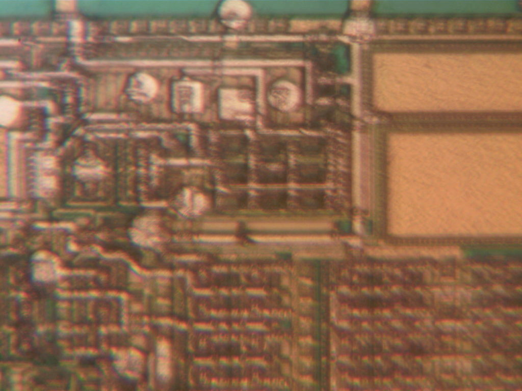
Reverse Chip ATmega461V and read mcu atmega461v flash Program, the fuse bit of atmega461v microcontroller will be broken to reset the status of MCU from locked to unlocked one;
The clock source for Timer/Counter2 is named clkT2S. clkT2S is by default connected to the main system I/O clock clkIO. By setting the AS2 bit in ASSR, Timer/Counter2 is asynchronously clocked from the TOSC1 pin.
This enables use of Timer/Counter2 as a Real Time Counter (RTC). When AS2 is set, pins TOSC1 and TOSC2 are disconnected from Port C if Reverse chip atmega861v code.
A crystal can then be connected between the TOSC1 and TOSC2 pins to serve as an independent clock source for Timer/Counter2. The Oscillator is optimized for use with a 32.768 kHz crystal. Applying an external clock source to TOSC1 is not recommended.
For Timer/Counter2, the possible prescaled selections are: clkT2S/8, clkT2S/32, clkT2S/64, clkT2S/128, clkT2S/256, and clkT2S/1024. Additionally, clkT2S as well as 0 (stop) may be selected after Reverse mcu atmega261 hex.
Setting the PSRASY bit in GTCCR resets the prescaler. This allows the user to operate with a predictable prescaler. When this bit is one, the Timer/Counter2 prescaler will be reset.
This bit is normally cleared immediately by hardware. If the bit is written when Timer/Counter2 is operating in asynchronous mode, the bit will remain one until the prescaler has been reset.
The bit will not be cleared by hardware if the TSM bit is set. Refer to the description of the “Bit 7– TSM: Timer/Counter Synchronization Mode” on page 170 for a description of the Timer/Counter Synchronization mode when Reverse CHIP PROGRAM.
The Serial Peripheral Interface (SPI) allows high-speed synchronous data transfer between the ATmega461v and peripheral devices or between several AVR devices. The ATmega640/1280/1281/2560/2561 SPI includes the following features:
Full-duplex, Three-wire Synchronous Data Transfer
Master or Slave Operation
LSB First or MSB First Data Transfer
Seven Programmable Bit Rates
End of Transmission Interrupt Flag
Write Collision Flag Protection
Wake-up from Idle Mode
Double Speed (CK/2) Master SPI Mode when Reverse CHIP PROGRAM
USART can also be used in Master SPI mode, see “USART in SPI Mode” on page 231. The Power Reduction SPI bit, PRSPI, in “Power Reduction Register 0 – PRR0” on page 54 on page 50 must be written to zero to enable SPI module.
Reverse MCU ATMEGA261 Heximal
We can Reverse Mcu ATMEGA261 Heximal, please view the Mcu ATMEGA261 features for your reference:
The N variable represents the prescale factor (1, 8, 32, 64, 128, 256, or 1024). The extreme values for the OCR2A Register represent special cases when generating a PWM waveform output in the fast PWM mode.
If the OCR2A is set equal to BOTTOM, the output will be a narrow spike for each MAX+1 timer clock cycle. Setting the OCR2A equal to MAX will result in a constantly high or low output (depending on the polarity of the output set by the COM2A1:0 bits.) when Reverse Mcu Heximal.
A frequency (with 50% duty cycle) waveform output in fast PWM mode can be achieved by setting OC2x to toggle its logical level on each compare match (COM2x1:0 = 1). The waveform generated will have a maximum frequency of foc2 = fclk_I/O/2 when OCR2A is set to zero if Reverse Mcu Heximal.
This feature is similar to the OC2A toggle in CTC mode, except the double buffer feature of the Output Compare unit is enabled in the fast PWM mode. The phase correct PWM mode (WGM22:0 = 1 or 5) provides a high resolution phase correct PWM waveform generation option before Reverse Mcu Heximal.
The phase correct PWM mode is based on a dual-slope operation. The counter counts repeatedly from BOTTOM to TOP and then from TOP to BOTTOM. TOP is defined as 0xFF when WGM22:0 = 1, and OCR2A when MGM22:0 = 5. In non-inverting Compare Output mode, the Output Compare (OC2x) is cleared on the compare match between TCNT2 and OCR2x while upcounting, and set on the compare match while downcounting after Reverse Mcu Heximal.
In inverting Output Compare mode, the operation is inverted. The dual-slope operation has lower maximum operation frequency than single slope operation. However, due to the symmetric feature of the dual-slope PWM modes, these modes are preferred for motor control applications if Reverse Mcu Heximal.
In phase correct PWM mode the counter is incremented until the counter value matches TOP. When the counter reaches TOP, it changes the count direction. The TCNT2 value will be equal to TOP for one timer clock cycle. The timing diagram for the phase correct PWM mode is shown on Figure 73 before Reverse Mcu Heximal.
The TCNT2 value is in the timing diagram shown as a histogram for illustrating the dual-slope operation. The diagram includes non-inverted and inverted PWM outputs. The small horizontal line marks on the TCNT2 slopes represent compare matches between OCR2x and TCNT2 when Reverse Mcu Heximal.
The Timer/Counter Overflow Flag (TOV2) is set each time the counter reaches BOTTOM. The Interrupt Flag can be used to generate an interrupt each time the counter reaches the BOTTOM value. In phase correct PWM mode, the compare unit allows generation of PWM waveforms on the OC2x pin. Setting the COM2x1:0 bits to two will produce a non-inverted PWM. An inverted PWM output can be generated by setting the COM2x1:0 to three. TOP is defined as 0xFF when WGM2:0 = 3, and OCR2A when MGM2:0 = 7 (See Table 87 on page 185). The actual OC2x value will only be visible on the port pin if the data direction for the port pin is set as output if Reverse Mcu Heximal.
The PWM waveform is generated by clearing (or setting) the OC2x Register at the compare match between OCR2x and TCNT2 when the counter increments, and setting (or clearing) the OC2x Register at compare match between OCR2x and TCNT2 when the counter decrements. The PWM frequency for the output when using phase correct PWM can be calculated by the following equation.
Posted in Recover MCU |
Tags: reverse mcu archive, reverse mcu binary, reverse mcu code, reverse mcu content, reverse mcu data, reverse mcu eeprom, reverse mcu file, reverse mcu firmware, reverse mcu hex, reverse mcu information, reverse mcu memory, reverse mcu program |
Comments Closed
Reverse Engineering Chip ATmega2560L Software
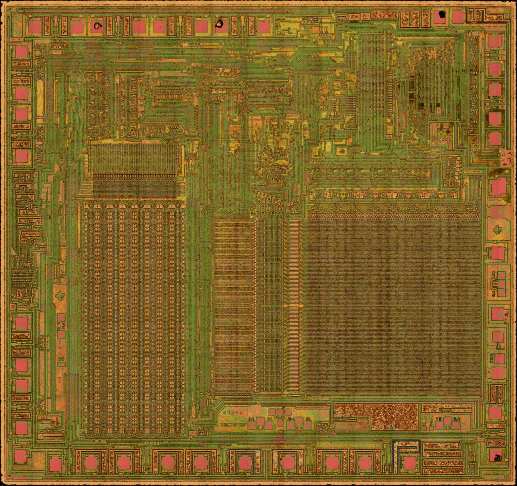
Reverse Engineering Chip ATmega2560L Software is actually a process to read encrypted heximal from mcu atmega2560L flash memory after crack microcontroller atmega2560L security fuse bit;
The Timer/Counter can be clocked by an internal synchronous or an external asynchronous clock source. The clock source clkT2 is by default equal to the MCU clock, clkI/O.
When the AS2 bit in the ASSR Register is written to logic one, the clock source is taken from the Timer/Counter Oscillator connected to TOSC1 and TOSC2. For details on asynchronous operation, see “Asynchronous Status Register – ASSR” on page 189 if attack attiny2313 mcu firmware.
For details on clock sources and prescaler, see “Timer/Counter Prescaler” on page 193. The main part of the 8-bit Timer/Counter is the programmable bi-directional counter unit.
Figure 68 shows a block diagram of the counter and its surrounding environment. Depending on the mode of operation used, the counter is cleared, incremented, or decremented at each timer clock (clkT2). clkT2 can be generated from an external or internal clock source, selected by the Clock Select bits (CS22:0) before attack atmega64l mcu flash.
When no clock source is selected (CS22:0 = 0) the timer is stopped. However, the TCNT2 value can be accessed by the CPU, regardless of whether clkT2 is present or not. A CPU write overrides (has priority over) all counter clear or count operations.
The counting sequence is determined by the setting of the WGM21 and WGM20 bits located in the Timer/Counter Control Register (TCCR2A) and the WGM22 located in the Timer/Counter Control Register B (TCCR2B).
There are close connections between how the counter behaves (counts) and how waveforms are generated on the Output Compare outputs OC2A and OC2B. For more details about advanced counting sequences and waveform generation, see “Modes of Operation” on page 178.
The Timer/Counter Overflow Flag (TOV2) is set according to the mode of operation selected by the WGM22:0 bits. TOV2 can be used for generating a CPU interrupt.
The 8-bit comparator continuously compares TCNT2 with the Output Compare Register (OCR2A and OCR2B). Whenever TCNT2 equals OCR2A or OCR2B, the comparator signals a match. A match will set the Output Compare Flag (OCF2A or OCF2B) at the next timer clock cycle.
If the corresponding interrupt is enabled, the Output Compare Flag generates an Output Compare interrupt. The Output Compare Flag is automatically cleared when the interrupt is executed.
Alternatively, the Output Compare Flag can be cleared by software by writing a logical one to its I/O bit location. The Waveform Generator uses the match signal to generate an output according to operating mode set by the WGM22:0 bits and Compare Output mode (COM2x1:0) bits.
The max and bottom signals are used by the Waveform Generator for handling the special cases of the extreme values in some modes of operation (“Modes of Operation” on page 178). Figure 58 on page 154 shows a block diagram of the Output Compare unit.
Posted in Recover MCU |
Tags: reverse engineering chip archive, reverse engineering chip binary, reverse engineering chip code, reverse engineering chip content, reverse engineering chip data, reverse engineering chip eeprom, reverse engineering chip file, reverse engineering chip firmware, reverse engineering chip heximal, reverse engineering chip information, reverse engineering chip memory, reverse engineering chip program |
Comments Closed
Reverse Engineering MCU ATmega1281P Firmware
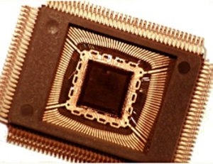
Reverse Engineering MCU ATmega1281P and copy embedded Firmware from microcontroller atmega1281p memory to new MCU, to make microprocessor atmega1281p cloning units.
The Timer/Counter Overflow Flag (TOVn) is set at the same timer clock cycle as the OCRnx Registers are updated with the double buffer value (at BOTTOM).
When either OCRnA or ICRn is used for defining the TOP value, the OCnA or ICFn Flag set when TCNTn has reached TOP. The Interrupt Flags can then be used to generate an interrupt each time the counter reaches the TOP or BOTTOM value.
When changing the TOP value the program must ensure that the new TOP value is higher or equal to the value of all of the Compare Registers. If the TOP value is lower than any of the Compare Registers, a compare match will never occur between the TCNTn and the OCRnx before attack microcontroller mc68hc705p6a memory.
As Figure 57 shows the output generated is, in contrast to the phase correct mode, symmetrical in all periods. Since the OCRnx Registers are updated at BOTTOM, the length of the rising and the falling slopes will always be equal. This gives symmetrical output pulses and is therefore frequency correct.
Using the ICRn Register for defining TOP works well when using fixed TOP values. By using ICRn, the OCRnA Register is free to be used for generating a PWM output on OCnA before copying pic16lf877 MCU program.
However, if the base PWM frequency is actively changed by changing the TOP value, using the OCRnA as TOP is clearly a better choice due to its double buffer feature.
In phase and frequency correct PWM mode, the compare units allow generation of PWM waveforms on the OCnx pins. Setting the COMnx1:0 bits to two will produce a non-inverted PWM and an inverted PWM output can be generated by setting the COMnx1:0 to three.
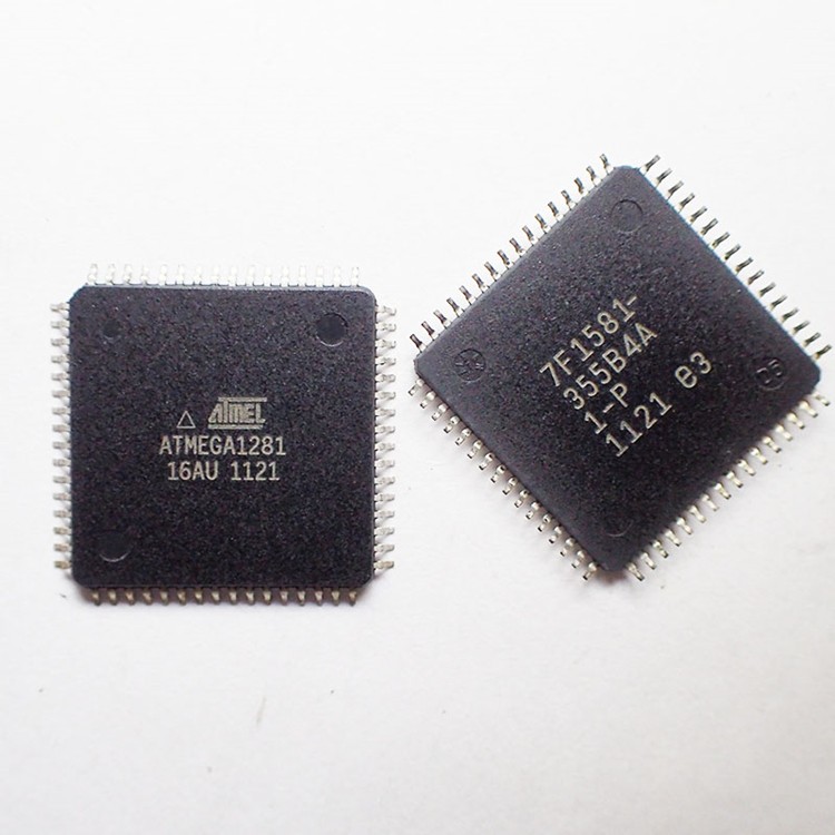
crack locked microcontroller ATMEGA1281 memory and clone its heximal file from program flash and data eeprom
The actual OCnx value will only be visible on the port pin if the data direction for the port pin is set as output (DDR_OCnx). The PWM waveform is generated by setting (or clearing) the OCnx Register at the compare match between OCRnx and TCNTn when the counter increments, and clearing (or setting) the OCnx Register at compare match between OCRnx and TCNTn when the counter decrements.
The PWM frequency for the output when using phase and frequency correct PWM can be calculated by the following equation:
The N variable represents the prescaler divider (1, 8, 64, 256, or 1024). The extreme values for the OCRnx Register represents special cases when generating a PWM waveform output in the phase correct PWM mode.
If the OCRnx is set equal to BOTTOM the output will be continuously low and if set equal to TOP the output will be set to high for non-inverted PWM mode. For inverted PWM the output will have the opposite logic values. If OCR1A is used to define the TOP value (WGM13:0 = 9) and COM1A1:0 = 1, the OC1A output will toggle with a 50% duty cycle.
Reverse Engineering MCU ATMEGA48P Program
Reverse Engineering MCU ATMEGA48P Program from flash memory and copy heximal program to new microcontroller atmega48p secured chipset;
Not all 16-bit accesses uses the Temporary Register for the high byte. Reading the OCRnA/B/C 16-bit registers does not involve using the Temporary Register, To do a 16-bit write, the high byte must be written before the low byte. For a 16-bit read, the low byte must be read before the high byte.
The following code examples show how to access the 16-bit timer registers assuming that no interrupts updates the temporary register. The same principle can be used directly for accessing the OCRnA/B/C and ICRn Registers. Note that when using “C”, the compiler handles the 16-bit access.
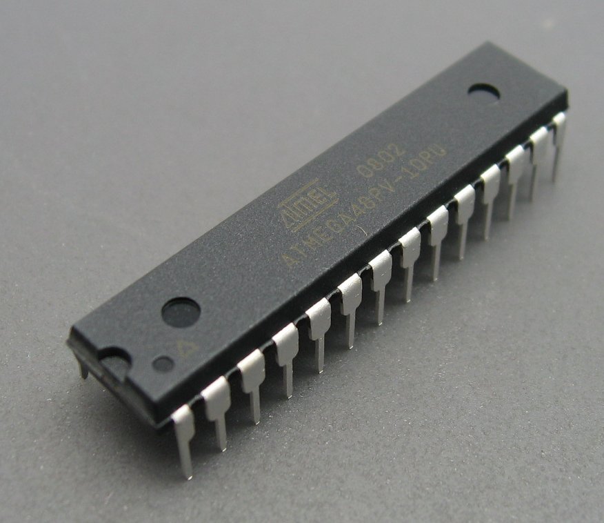
unlock encrypted atmega48pv microcontroller protective system and dump embedded heximal file from flash memory
The assembly code example returns the TCNTn value in the r17:r16 register pair. It is important to notice that accessing 16-bit registers are atomic operations when breaking microcontroller atmega48p atmel avr chip fuse bit. If an interrupt occurs between the two instructions accessing the 16-bit register, and the interrupt code updates the temporary register by accessing the same or any other of the 16-bit Timer Registers, then the result of the access outside the interrupt will be corrupted.
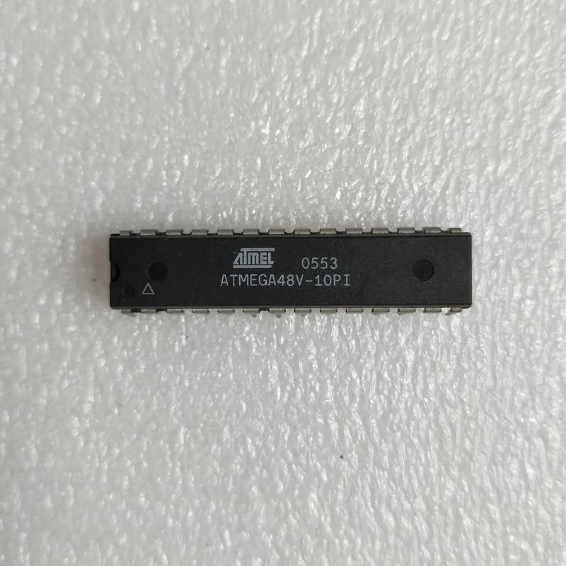
crack secured mcu atmega48v fuse bit and extract embedded heximal file from flash memory
Therefore, when both the main code and the interrupt code update the temporary register, the main code must disable the interrupts during the 16-bit access after readout microcontroller atmega48pa binary file and heximal from eeprom and flash memory. The following code examples show how to do an atomic read of the TCNTn Register contents. Reading any of the OCRnA/B/C or ICRn Registers can be done by using the same principle.
If writing to more than one 16-bit register where the high byte is the same for all registers written, then the high byte only needs to be written once. However, note that the same rule of atomic operation described previously also applies in this case.
Recover Chip ATmega128PV Flash
We can Recover CHIP ATMEGA128PV Flash, please view the CHIP ATMEGA128PV features for your reference:
The simplest mode of operation is the Normal mode (WGMn3:0 = 0). In this mode the counting direction is always up (incrementing), and no counter clear is performed.
The counter simply overruns when it passes its maximum 16-bit value (MAX = 0xFFFF) and then restarts from the BOTTOM (0x0000).
In normal operation the Timer/Counter Over-flow Flag (TOVn) will be set in the same timer clock cycle as the TCNTn becomes zero.
The TOVn Flag in this case behaves like a 17th bit, except that it is only set, not cleared. However, combined with the timer overflow interrupt that automatically clears the TOVn Flag, the timer resolution can be increased by software.
There are no special cases to consider in the Normal mode, a new counter value can be written anytime. The Input Capture unit is easy to use in Normal mode. However, observe that the maximum interval between the external events must not exceed the resolution of the counter.
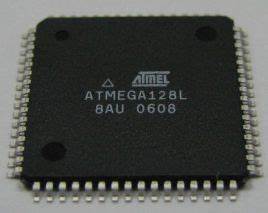
Recover Chip ATmega128PV Flash
If the interval between events are too long, the timer overflow interrupt or the prescaler must be used to extend the resolution for the capture unit. The Output Compare units can be used to generate interrupts at some given time.
Using the Output Compare to generate waveforms in Normal mode is not recommended, since this will occupy too much of the CPU time. In Clear Timer on Compare or CTC mode (WGMn3:0 = 4 or 12), the OCRnA or ICRn Register are used to manipulate the counter resolution.
In CTC mode the counter is cleared to zero when the counter value (TCNTn) matches either the OCRnA (WGMn3:0 = 4) or the ICRn (WGMn3:0 = 12). The OCRnA or ICRn define the top value for the counter, hence also its resolution.
This mode allows greater control of the compare match output frequency. It also simplifies the operation of counting external events. The timing diagram for the CTC mode is shown in Figure 54. The counter value (TCNTn) increases until a compare match occurs with either OCRnA or ICRn, and then counter (TCNTn) is cleared.
An interrupt can be generated at each time the counter value reaches the TOP value by either using the OCFnA or ICFn Flag according to the register used to define the TOP value. If the interrupt is enabled, the interrupt handler routine can be used for updating the TOP value. However, changing the TOP to a value close to BOTTOM when the counter is running with none or a low prescaler value must be done with care since the CTC mode does not have the double buffering feature.
If the new value written to OCRnA or ICRn is lower than the current value of TCNTn, the counter will miss the compare match. The counter will then have to count to its maximum value (0xFFFF) and wrap around starting at 0x0000 before the compare match can occur. In many cases this feature is not desirable. An alternative will then be to use the fast PWM mode using OCRnA for defining TOP (WGMn3:0 = 15) since the OCRnA then will be double buffered.
For generating a waveform output in CTC mode, the OCnA output can be set to toggle its logical level on each compare match by setting the Compare Output mode bits to toggle mode (COMnA1:0 = 1). The OCnA value will not be visible on the port pin unless the data direction for the pin is set to output (DDR_OCnA = 1).
The waveform generated will have a maximum frequency of fOCnA = fclk_I/O/2 when OCRnA is set to zero (0x0000). The waveform frequency is defined by the following equation.
Recover Chip ATmega640P Heximal
Recover Chip ATmega640P Heximal from Microcontroller ATmega640P flash and eeprom memory, rewrite the firmware to blank MCU ATmega640P by Microprocessor copying technique, unlock MCU secured system and reset the status of Microcontroller from locked to unlocked;
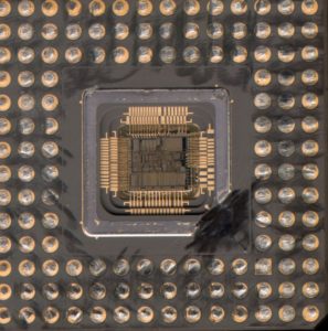
Recover Chip ATmega640P Heximal from Microcontroller ATmega640P flash and eeprom memory, rewrite the firmware to blank MCU ATmega640P by Microprocessor copying technique, unlock MCU secured system and reset the status of Microcontroller from locked to unlocked
In non-PWM waveform generation modes, the match output of the comparator can be forced by writing a one to the Force Output Compare (FOC0x) bit. Forcing Compare Match will not set the OCF0x Flag or reload/clear the timer, but the OC0x pin will be updated as if a real Compare Match had occurred (the COM0x1:0 bits settings define whether the OC0x pin is set, cleared or toggled) if MCU PIC16F917 heximal breaking.
All CPU write operations to the TCNT0 Register will block any Compare Match that occur in the next timer clock cycle, even when the timer is stopped. This feature allows OCR0x to be initialized to the same value as TCNT0 without triggering an interrupt when the Timer/Counter clock is enabled.
Since writing TCNT0 in any mode of operation will block all Compare Matches for one timer clock cycle, there are risks involved when changing TCNT0 when using the Output Compare Unit, independently of whether the Timer/Counter is running or not after recover MCU PIC16F72 code.
If the value written to TCNT0 equals the OCR0x value, the Compare Match will be missed, resulting in incorrect waveform generation. Similarly, do not write the TCNT0 value equal to BOTTOM when the counter is down-counting.
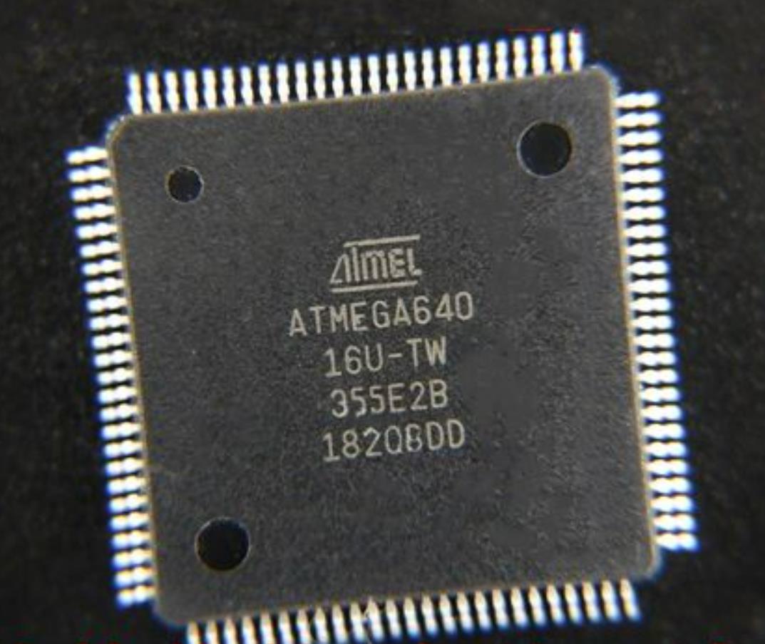
microprocessor atmega640v protection unlocking and readout embedded firmware
The setup of the OC0x should be performed before setting the Data Direction Register for the port pin to output. The easiest way of setting the OC0x value is to use the Force Output Compare (FOC0x) strobe bits in Normal mode if recover MCU PIC16F77 eeprom heximal.
The OC0x Registers keep their values even when changing between Waveform Generation modes. Be aware that the COM0x1:0 bits are not double buffered together with the compare value. Changing the COM0x1:0 bits will take effect immediately.
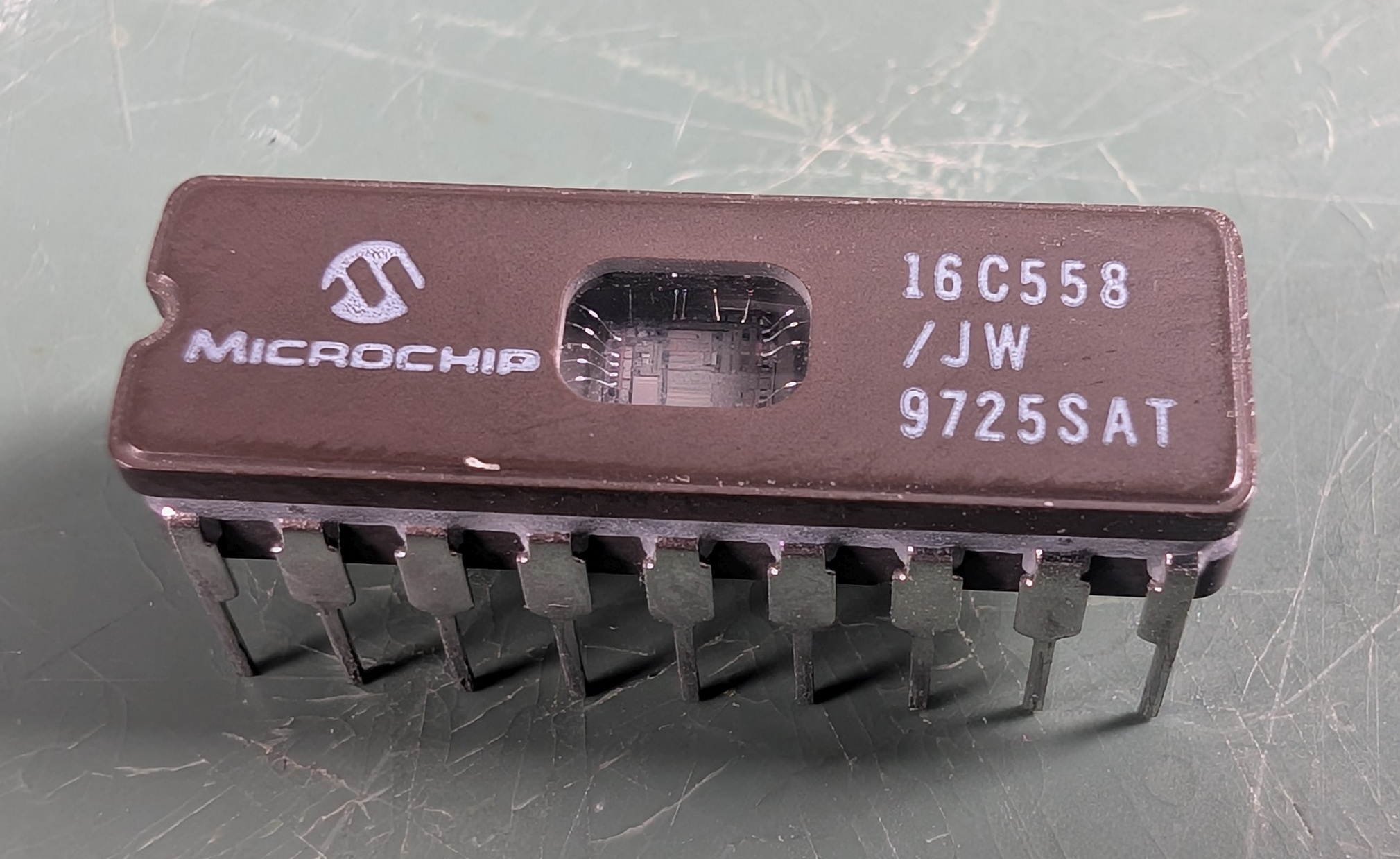
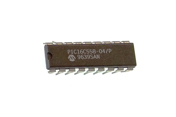
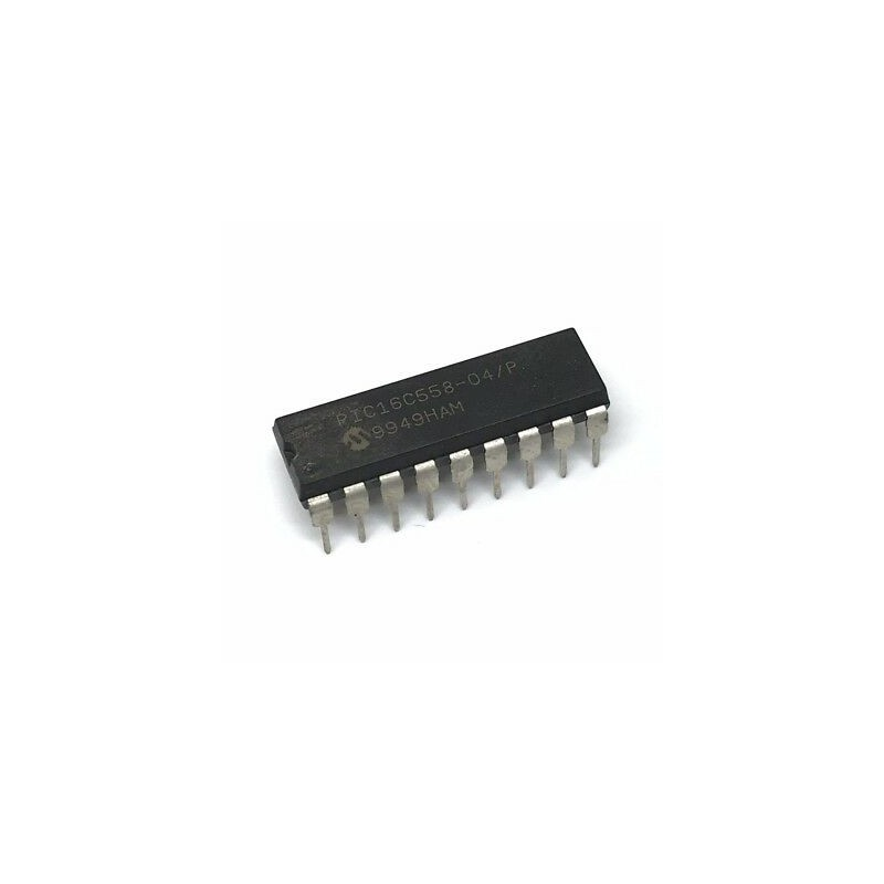
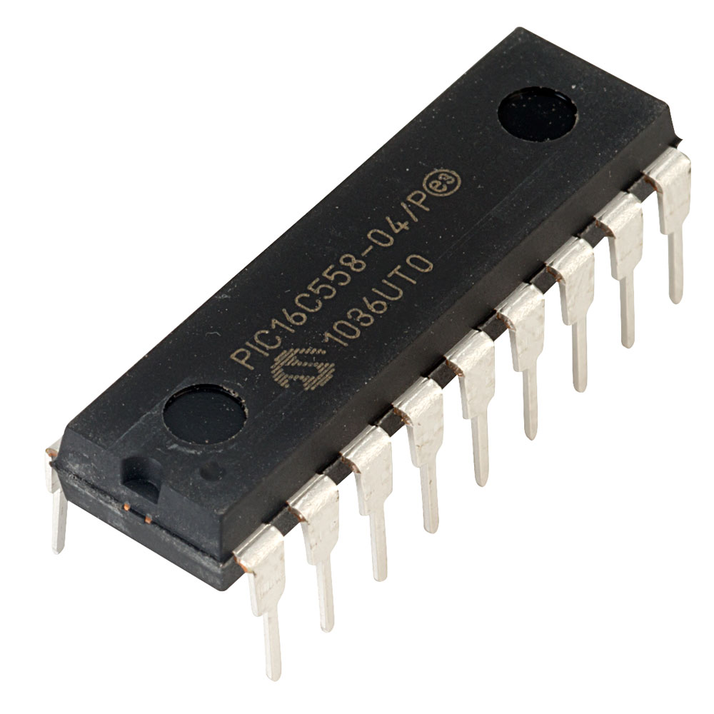
Attack MCU PIC16C558 Program
The PIC16C558 is a widely deployed microcontroller designed for cost-sensitive yet reliable embedded applications. Unlike a PLD, this MCU integrates processing capability with on-chip memory, making it ideal for consumer electronics, industrial control units, home appliances, automotive subsystems, and security devices. Its architecture allows compact storage of operational firmware, including control program logic and essential data within internal EPROM/EEPROM-like memory structures. In most production environments, the source code, binary, or heximal file embedded inside the chip is deliberately protected, locked, or encrypted to prevent duplication and safeguard intellectual property. However, this also creates challenges when original design archives are lost or when long-term system maintenance is required.
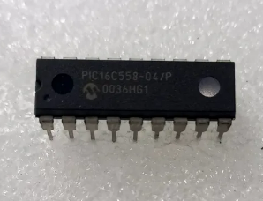
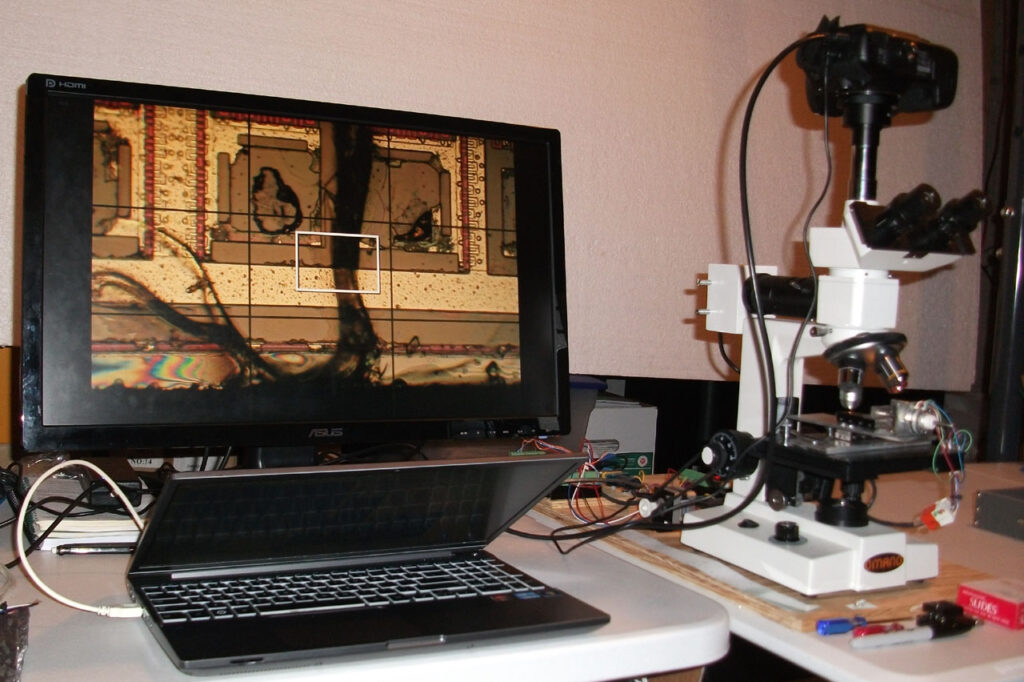
Our “Attack MCU PIC16C558 Program” service is built to attack, break, and decode these secured microcontrollers with precision and reliability. By leveraging advanced decapsulate techniques combined with electrical fault analysis, we are able to retrieve internal memory content, including firmware, structured binary, and heximal data files. Even when the MCU is heavily protected or features multiple layers of encryption, our engineers can effectively hack through these barriers to extract usable data archives. The recovered program file is then reconstructed into readable source code, allowing clients to fully understand and reuse the original design. This enables seamless clone and duplicate operations, whether for legacy product support, compatibility upgrades, or reverse engineering analysis of existing systems.
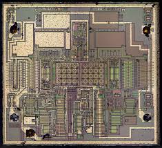
Attack MCU PIC16C558 secured system by disable the security fuse bit embedded in the microcontroller PIC16C558 , extract microprocessor program and data from flash memory;
The UV erasable version, offered in CERDIP package is optimal for prototype development and pilot programs. This version can be erased and reprogrammed to any of the oscillator modes.
Microchip offers a QTP Programming Service for factory production orders. This service is made available for users who choose not to program a medium to high quantity of units and whose code patterns have stabilized when Attack MCU. The devices are identical to the OTP devices but with all EPROM locations and configuration options already programmed by the factory. Certain code and prototype verification procedures apply before production shipments are available.
Microchip offers a unique programming service where a few user-defined locations in each device are programmed with different serial numbers. The serial numbers may be random, pseudo-random or sequential. The high performance of the PIC16C55X(A) family can be attributed to a number of architectural features commonly found in RISC microprocessors.
To begin with, the PIC16C55X(A) uses a Harvard architecture, in which, program and data are accessed from separate memories using separate busses after Attack MCU. This improves bandwidth over traditional von Neumann architecture where program and data are fetched from the same memory. Separating program and data memory further allows instructions to be sized differently than 8-bit wide data words. Instruction opcodes are 14-bits wide making it possible to have all single word instructions.
A 14-bit wide program memory access bus fetches a 14-bit instruction in a single cycle. A two-stage pipeline overlaps fetch and execution of instructions. Consequently, all instructions (35) execute in a single-cycle (200 ns @ 20 MHz) except for program branches.
The PIC16C554(A) addresses 512 x 14 on-chip program memory. The PIC16C556A addresses 1K x 14 program memory. The PIC16C558(A) addresses 2K x 14 program memory. All program memory is internal. The PIC16C55X(A) can directly or indirectly address its register files or data memory.
All special function registers including the program counter are mapped into the data memory. The PIC16C55X(A) have an orthogonal (symmetrical) instruction set that makes it possible to carry out any operation on any register using any addressing mode. This symmetrical nature and lack of ‘special optimal situations’ make programming with the PIC16C55X(A) simple yet efficient. In addition, the learning curve is reduced significantly.
The availability of OTP devices is especially useful for customers who need the flexibility for frequent code updates and small volume applications. In addition to the program memory, the configuration bits must also be programmed.
From a technical workflow perspective, the process combines silicon-level access with sophisticated decode algorithms. During decapsulation, the chip package is carefully opened to expose the die, enabling direct probing and controlled retrieval of embedded data from internal memory cells. The extracted binary is then processed through proprietary tools that translate raw data into structured firmware archives, ensuring that each file is complete and logically consistent. This hybrid methodology allows us to overcome even highly secured and encrypted configurations, delivering not just raw dumps but fully interpretable program structures. Through careful validation, we ensure the reconstructed source code accurately reflects the original MCU behavior, making it suitable for redevelopment or system integration.
The ability to attack, decode, and recover a locked PIC16C558 brings significant advantages to end users across multiple industries. Companies facing discontinued components, unavailable documentation, or supply chain disruptions can regain control over critical firmware and data assets without costly redesigns. By extracting and duplicating the original program, clients can extend product lifecycles, maintain system compatibility, and accelerate engineering workflows. Ultimately, our service transforms inaccessible embedded memory into actionable knowledge, providing a dependable pathway to restore, analyze, and replicate the functional core of PIC-based systems with confidence and efficiency.
Attack MCU AT91SAM7S256 Binary
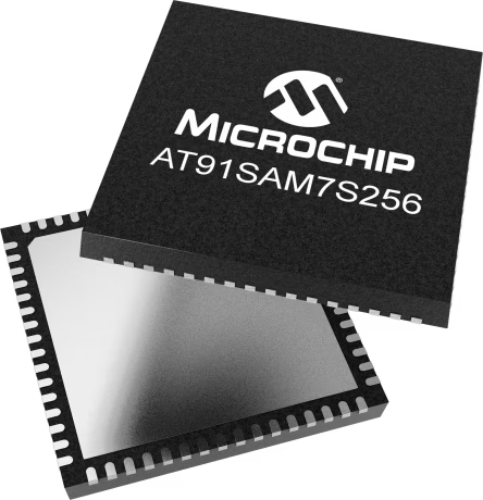
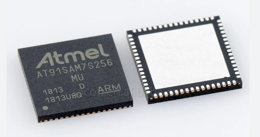
The AT91SAM7S256 is a widely deployed ARM7TDMI-based microcontroller that has earned a strong reputation across industrial control, consumer electronics, automotive peripherals, access control, and embedded instrumentation. With 256 KB on-chip flash, integrated SRAM, multiple communication interfaces, and low-power embedded operation, it has been adopted in products where long life cycles and firmware stability are critical. In many real-world scenarios, however, manufacturers or maintenance teams face situations such as discontinued suppliers, missing documentation, or protected devices that can no longer be updated through official channels. This is where professional services centered on Attack MCU AT91SAM7S256 Binary become essential for legitimate analysis, refurbishment, and product continuity.
In practical projects, the firmware, binary, or heximal file stored in the flash and EEPROM of the AT91SAM7S256 is often protected, locked, or secured by design. Our service focuses on controlled methods to attack, break, or hack these protection mechanisms at a conceptual level in order to retrieve embedded firmware data safely and reliably. Through advanced lab techniques, we help customers decode encrypted or locked memory regions, reconstruct usable firmware archives, and recover critical program files when the original source code has been lost. In special cases, decapsulation may be applied as part of failure analysis to access deeply embedded memory structures, always with strict process control. The end result is the ability to extract binary, flash, or EEPROM data archives from embedded systems that were previously considered unreachable.
Once firmware data has been successfully retrieved, our engineers assist in transforming raw memory dumps into structured, usable assets. This includes rebuilding firmware images, analyzing binary and heximal content, and correlating data with application logic so customers can clone or duplicate functional behavior for maintenance, compatibility testing, or redesign. By working at the firmware, source code reconstruction, and program file level, we enable customers to understand how encrypted or protected embedded systems operate without requiring original development files. This approach is especially valuable for industrial equipment, medical devices, and automation controllers where replacing hardware is costly, yet firmware updates or security audits are unavoidable.
Ultimately, the purpose of an Attack MCU AT91SAM7S256 Binary service is not destruction, but preservation and enhancement of embedded assets. End users benefit from extended product life, reduced downtime, and the ability to migrate legacy designs onto new platforms while retaining proven functionality. Whether the goal is refurbishment, compliance verification, data recovery, or controlled duplication of embedded firmware behavior, our service provides a professional and discreet path forward. By combining deep MCU knowledge with experience in protected, encrypted, and secured embedded environments, we help customers regain control over their firmware, memory, and data—turning locked devices back into manageable engineering resources.
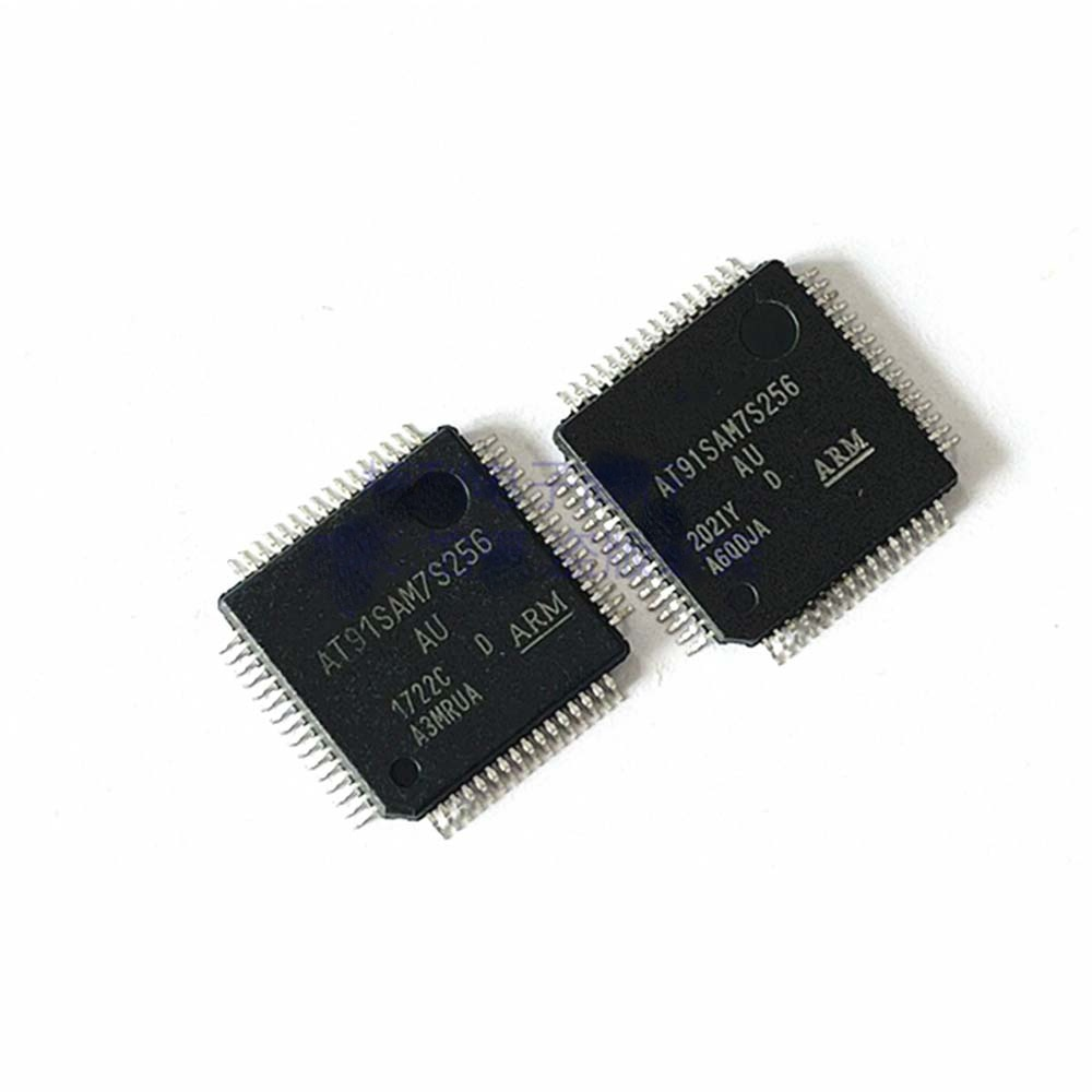
In the world of embedded systems, security measures such as encryption, locking mechanisms, and readout protection are often deployed to safeguard proprietary code and prevent unauthorized access. However, in legitimate scenarios like legacy system recovery, custom development, or system maintenance, the need to attack MCU AT91SAM7S256 binary becomes critical.
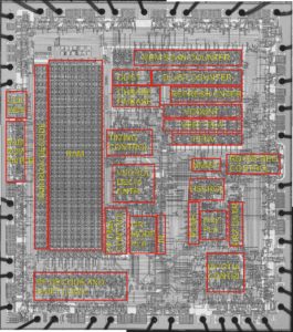
· Incorporates the ARM7TDMI® ARM® Thumb® Processor
– High-performance 32-bit RISC Architecture
– High-density 16-bit Instruction Set
– Leader in MIPS/Watt
– Embedded*ICE™ In-circuit Emulation, Debug Communication Channel Support
Internal High-speed Flash
– 256 kbytes, organized in 1024 Pages of 256 Bytes (AT91SAM7S256)
– 128 kbytes, organized in 512 Pages of 256 Bytes (AT91SAM7S128)
– 64 kbytes, organized in 512 Pages of 128 Bytes (AT91SAM7S64)
– 32 kbytes, organized in 256 Pages of 128 Bytes (AT91SAM7S321/32)
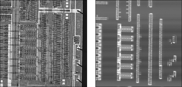
– Single Cycle Access at Up to 30 MHz in Worst Case Conditions
– Prefetch Buffer Optimizing Thumb Instruction Execution at Maximum Speed after break avr atmega64a MCU
– Page Programming Time: 6 ms, Including Page Auto-erase, Full Erase Time: 15 ms
– 10,000 Write Cycles, 10-year Data Retention Capability, Sector Lock Capabilities,
Flash Security Bit
– Fast Flash Programming Interface for High Volume Production
Internal High-speed SRAM, Single-cycle Access at Maximum Speed
– 64 kbytes (AT91SAM7S256)
– 32 kbytes (AT91SAM7S128)
– 16 kbytes (AT91SAM7S64)
– 8 kbytes (AT91SAM7S321/32)
Memory Controller (MC)
– Embedded Flash Controller, Abort Status and Misalignment Detection
Reset Controller (RSTC)
– Based on Power-on Reset and Low-power Factory-calibrated Brown-out Detector
– Provides External Reset Signal Shaping and Reset Source Status
Clock Generator (CKGR)
– Low-power RC Oscillator, 3 to 20 MHz On-chip Oscillator and one PLL
Power Management Controller (PMC)
– Software Power Optimization Capabilities, Including Slow Clock Mode (Down to 500 Hz) and Idle Mode
– Three Programmable External Clock Signals
Advanced Interrupt Controller (AIC)
– Individually Maskable, Eight-level Priority, Vectored Interrupt Sources
– Two (AT91SAM7S256/128/64/321) or One (AT91SAM7S32) External Interrupt Sources and One Fast Interrupt Source, Spurious Interrupt Protected Debug Unit (DBGU)
– 2-wire UART and Support for Debug Communication Channel interrupt,
Programmable ICE Access Prevention by break microcontroller atmega128 hex
Periodic Interval Timer (PIT)
– 20-bit Programmable Counter plus 12-bit Interval Counter Windowed Watchdog (WDT)
– 12-bit key-protected Programmable Counter
– Provides Reset or Interrupt Signals to the System
– Counter May Be Stopped While the Processor is in Debug State or in Idle Mode
Eleven (AT91SAM7S256/128/64/321) or Nine (AT91SAM7S32) Peripheral DMA Controller (PDC) Channels
One USB 2.0 Full Speed (12 Mbits per Second) Device Port (Except for the AT91SAM7S32).
– On-chip Transceiver, 328-byte Configurable Integrated FIFOs
One Synchronous Serial Controller (SSC)
– Independent Clock and Frame Sync Signals for Each Receiver and Transmitter
– I²S Analog Interface Support, Time Division Multiplex Support
– High-speed Continuous Data Stream Capabilities with 32-bit Data Transfer
Two (AT91SAM7S256/128/64/321) or One (AT91SAM7S32) Universal Synchronous/Asynchronous Receiver Transmitters (USART)
– Individual Baud Rate Generator, IrDA® Infrared Modulation/Demodulation
– Support for ISO7816 T0/T1 Smart Card, Hardware Handshaking, RS485 Support
– Manchester Encoder/Decoder (AT91SAM7S256/128)
– Full Modem Line Support on USART1 (AT91SAM7S256/128/64/321)
One Master/Slave Serial Peripheral Interface (SPI)
– 8- to 16-bit Programmable Data Length, Four External Peripheral Chip Selects
One Three (AT91SAM7S256/128/64/321)-channel or Two (AT91SAM7S32)-channel 16-bit Timer/Counter (TC)
– Three (AT91SAM7S256/128/64/321) or One (AT91SAM7S32) External Clock Inputs, Two Multi-purpose I/O Pins per Channel before Attack MCU
– Double PWM Generation, Capture/Waveform Mode, Up/Down Capability
One Four-channel 16-bit PWM Controller (PWMC)
One Two-wire Interface (TWI)
– Master Mode Support Only, All Two-wire Atmel EEPROMs Supported
One 8-channel 10-bit Analog-to-Digital Converter, Four Channels Multiplexed with Digital I/Os
SAM-BA™ Boot Assistant
– Default Boot program
– Interface with SAM-BA Graphic User Interface
IEEE 1149.1 JTAG Boundary Scan on All Digital Pins if Attack MCU
5V-tolerant I/Os, including Four High-current Drive I/O lines, Up to 16 mA Each
Power Supplies
– Embedded 1.8V Regulator, Drawing up to 100 mA for the Core and External Components
– 3.3V or 1.8V VDDIO I/O Lines Power Supply, Independent 3.3V VDDFLASH Flash Power Supply
– 1.8V VDDCORE Core Power Supply with Brown-out Detector
Fully Static Operation: Up to 55 MHz at 1.65V and 85° C Worst Case Conditions
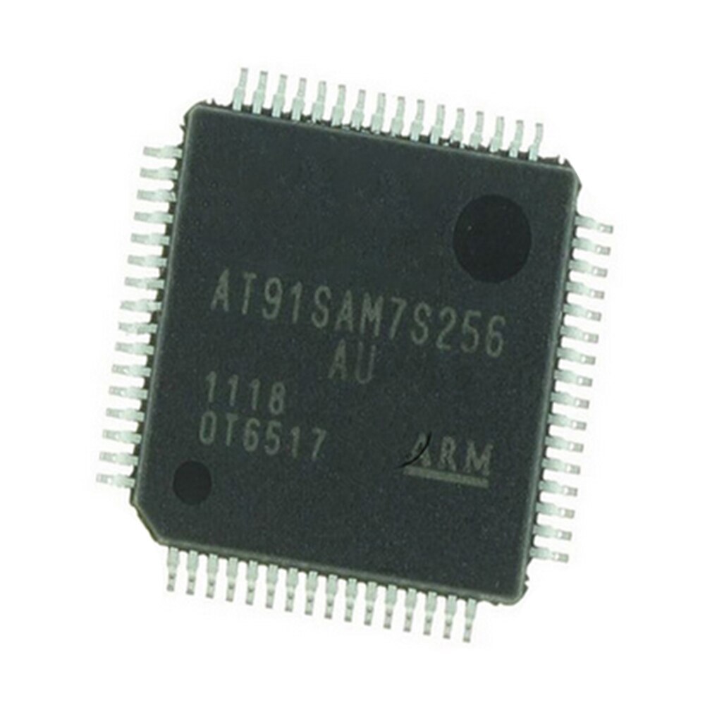
Available in a 64-lead LQFP Green Package (AT91SAM7S256/128/64/321) and 48-lead LQFP Green Package (AT91SAM7S32).