Archive for the ‘Recover MCU’ Category
 Attack CPLD XC9536XL-10VQG44C Software
 August 4th, 2010 |
  Author:
 The CPLD XC9536XL-10VQG44C is a widely adopted PLD device known for its reliability, low power consumption, and flexible logic configuration in embedded systems. Commonly deployed across industrial automation, medical instrumentation, automotive control modules, and communication equipment, this component plays a critical role in managing timing logic, signal routing, and interface control. Its compact architecture and non-volatile memory make it ideal for applications requiring stable and repeatable execution of embedded program logic. However, in many scenarios, the internal firmware or source code stored inside the chip is protected, locked, or even encrypted, preventing direct access to valuable data, binary, or heximal design files.
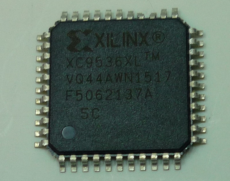
Our specialized service for “Attack CPLD XC9536XL-10VQG44C Software” is designed to attack, break, and decode these secured devices in a controlled and professional manner. Through advanced techniques such as decapsulate processes, electrical analysis, and protocol-level exploitation, we are able to retrieve critical firmware, extract binary or heximal file structures, and reconstruct the original source code or logic configuration. Whether the target is stored in internal flash, EEPROM, or embedded memory, our engineers can effectively hack through multiple layers of protective and secured mechanisms. The extracted data archive can then be analyzed, allowing clients to clone, duplicate, or redevelop the original program with high accuracy. This process ensures that even heavily encrypted or locked CPLD devices can be transformed into accessible engineering resources.
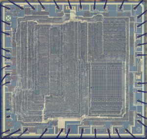
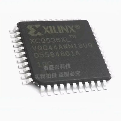
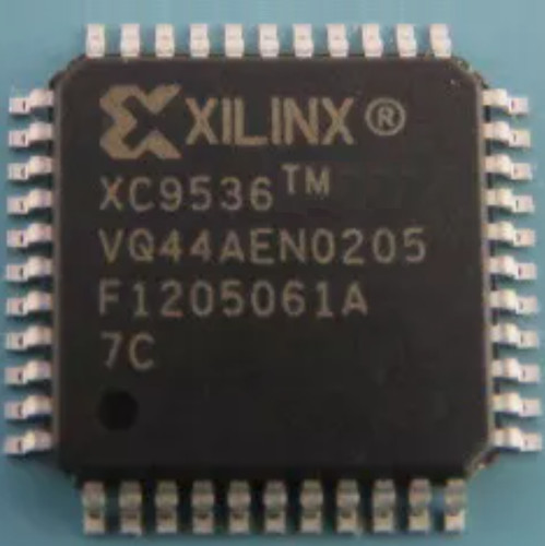
We can Attack CPLD XC9536XL-10VQG44C Software, please view below CPLD XC9536XL-10VQG44C features for your reference:
Features
· 5 ns pin-to-pin logic delays
· System frequency up to 178 MHz
Product Specification
54V18 Function Blocks, providing 800 usable gates with propagation delays of 5 ns. See Figure 2 for architecture overview.
36 macrocells with 800 usable gates
Available in small footprint packages
– 44-pin PLCC (34 user I/O pins)
– 44-pin VQFP (34 user I/O pins)
– 48-pin CSP (36 user I/O pins)
– 64-pin VQFP (36 user I/O pins)
– Pb-free available for all packages
Optimized for high-performance 3.3V systems
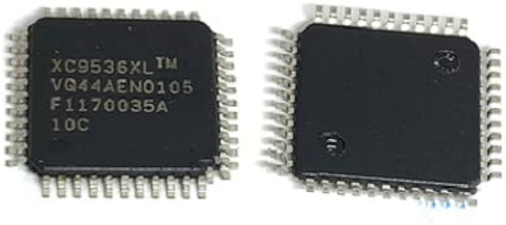
– Low power operation
– 5V tolerant I/O pins accept 5 V, 3.3V, and 2.5V signals
– 3.3V or 2.5V output capability
– Advanced 0.35 micron feature size CMOS Fast FLASH™ technology
Advanced system features
– In-system programmable
– Superior pin-locking and routability with
Fast CONNECT™ II switch matrix
– Extra wide 54-input Function Blocks
– Up to 90 product-terms per macrocell with individual product-term allocation
– Local clock inversion with three global and one product-term clocks
– Individual output enable per output pin
– Input hysteresis on all user and boundary-scan pin inputs
– Bus-hold circuitry on all user pin inputs
– Full IEEE Standard 1149.1 boundary-scan (JTAG)
Fast concurrent programming
Slew rate control on individual outputs
Enhanced data security features
Excellent quality and reliability
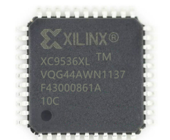
– Endurance exceeding 10,000 program/erase cycles
– 20 year data retention
– ESD protection exceeding 2,000V
Pin-compatible with 5V-core XC9536 device in the
Power Estimation
Power dissipation in CPLDs can vary substantially depending on the system frequency, design application and output loading when Attack CPLD. To help reduce power dissipation, each macrocell in a XC9500XL device may be configured for low-power mode (from the default high-performance mode).
In addition, unused product-terms and macrocells are automatically deactivated by the software to further conserve power.
For a general estimate of ICC, the following equation may be used:
ICC(mA) = MCHS(0.175*PTHS + 0.345) + MCLP(0.052*PTLP + 0.272) + 0.04 * MCTOG(MCHS +MCLP)* where if Attack CPLD:
MCHS = # macrocells in high-speed configuration
PTHS = average number of high-speed product terms per macrocell
MCLP = # macrocells in low power configuration
PTLP = average number of low power product terms per macrocell
f = maximum clock frequency
MCTOG = average % of flip-flops toggling per clock (~12%)
This calculation was derived from laboratory measurements of an XC9500XL part filled with 16-bit counters and allowing
a single output (the LSB) to be enabled. The actual ICC value varies with the design application and should be verified during normal system operation. Figure 1 shows the above estimation in a graphical form. For a more detailed discussion of power consumption in this device, see Xilinx 44-pin PLCC package and the 48-pin CSP package.
WARNING: Programming temperature range of TA = 0° C to +70° C
Description
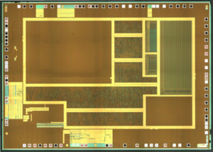
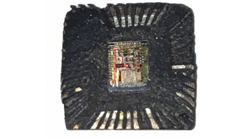
Technically, the workflow involves both physical and logical approaches. On the physical level, decapsulation exposes the silicon die for direct probing, while non-invasive methods may also be applied to decode configuration bits. On the logical level, we utilize proprietary algorithms to reconstruct firmware structures from raw binary dumps, converting them into usable source code or structured data files. This enables efficient retrieval and validation of embedded logic. By combining these approaches, we ensure a high success rate in breaking protection schemes and delivering accurate archive outputs. Clients can then clone or duplicate the CPLD design for maintenance, redesign, or compatibility upgrades without needing the original development files.
The demand for such services continues to grow as industries face challenges like component obsolescence, lack of documentation, and supply chain disruptions. By leveraging our capability to attack, decode, and restore secured CPLD memory, end users gain full control over their hardware assets. This not only reduces redevelopment costs but also accelerates product lifecycle management. Whether the goal is to recover lost firmware, analyze a competitor’s embedded design, or replicate a legacy system, our service provides a reliable pathway to access, understand, and reuse critical data locked within the XC9536XL-10VQG44C.
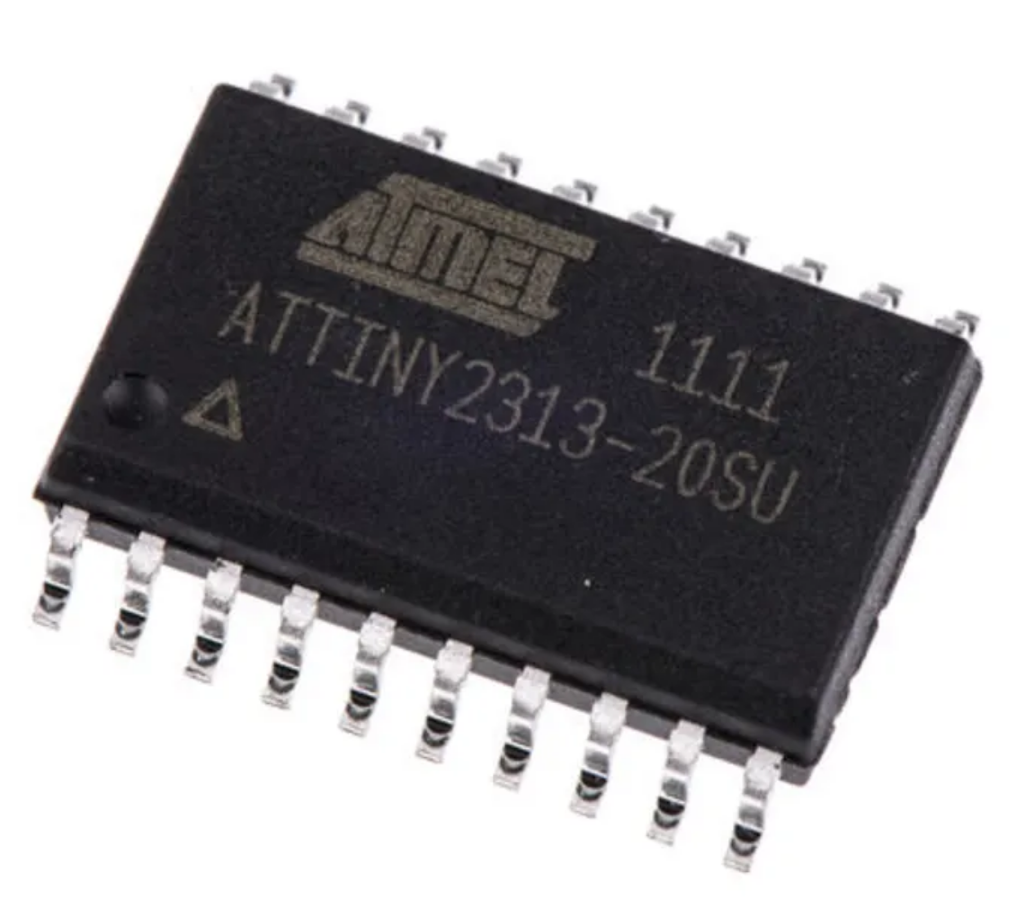
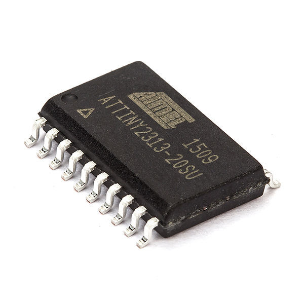
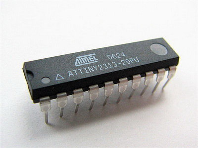
Attack Chip ATtiny2313 Firmware
Attack Chip ATtiny2313 and extract mcu attiny2313 Firmware from flash and eeprom memory in the format of heximal, unlock microcontroller attiny2313 fuse bit by focus ion beam;
Features
· High Performance, Low Power AVR 8-Bit Microcontroller
· Advanced RISC Architecture
– 120 Powerful Instructions – Most Single Clock Cycle Execution
– 32 x 8 General Purpose Working Registers
– Fully Static Operation
– Up to 20 MIPS Throughput at 20 MHz
Data and Non-volatile Program and Data Memories if break mcu pic16f631 flash
– 2/4K Bytes of In-System Self Programmable Flash
· Endurance 10,000 Write/Erase Cycles
– 128/256 Bytes In-System Programmable EEPROM
· Endurance: 100,000 Write/Erase Cycles
Technical Methodology for Firmware Analysis
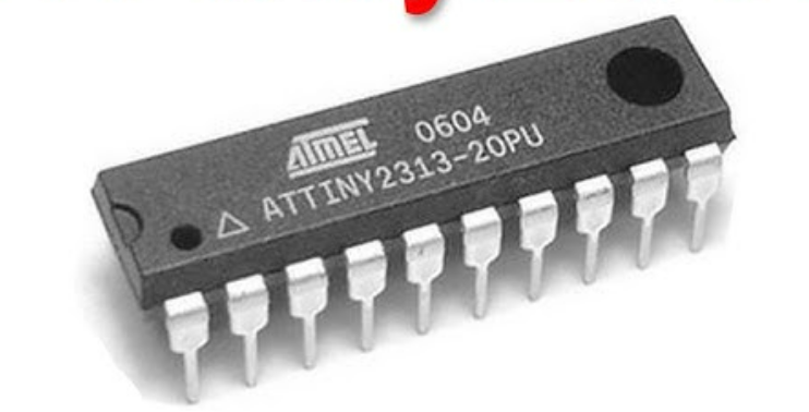
Our firmware analysis process for ATtiny2313 devices follows a structured, non-destructive methodology. We begin with comprehensive examination of the microcontroller’s configuration, analyzing fuse bit settings and lock bit configurations to understand the specific security implementation. This initial assessment determines the appropriate technical approach for accessing the protected memory contents.
For devices where security features have been enabled, we employ specialized hardware interfaces and signal analysis techniques to establish controlled communication with the microcontroller’s internal systems. This process requires precise timing control and deep understanding of AVR architecture to navigate around protective barriers without triggering permanent lockout mechanisms or damaging the physical device . The goal is to extract the complete firmware image while preserving both the microcontroller’s integrity and the recovered data’s accuracy.
– 128/256 Bytes Internal SRAM
– Programming Lock for Flash Program and EEPROM Data Security
Peripheral Features
– One 8-bit Timer/Counter with Separate Prescaler and Compare Mode
– One 16-bit Timer/Counter with Separate Prescaler, Compare and Capture Modes
– Four PWM Channels
– On-chip Analog Comparator
– Programmable Watchdog Timer with On-chip Oscillator
– USI – Universal Serial Interface
– Full Duplex USART
Special Microcontroller Features
– debugWIRE On-chip Debugging
– In-System Programmable via SPI Port
– External and Internal Interrupt Sources
– Low-power Idle, Power-down, and Standby Modes when Attack mcu pic12f510 program
– Enhanced Power-on Reset Circuit
– Programmable Brown-out Detection Circuit
– Internal Calibrated Oscillator
I/O and Packages
– 18 Programmable I/O Lines
– 20-pin PDIP, 20-pin SOIC, 20-pad MLF/VQFN
Operating Voltage
– 1.8 – 5.5V
Speed Grades
– 0 – 4 MHz @ 1.8 – 5.5V
– 0 – 10 MHz @ 2.7 – 5.5V
– 0 – 20 MHz @ 4.5 – 5.5V
Industrial Temperature Range: -40°C to +85°C
Low Power Consumption
– Active Mode
· 190 µA at 1.8V and 1MHz
– Idle Mode
· 24 µA at 1.8V and 1MHz
– Power-down Mode
· 0.1 µA at 1.8V and +25°C
Firmware Extraction and Binary Recovery
Once access is established, our equipment performs a complete memory read operation, capturing every byte stored within the ATtiny2313’s Flash program memory and EEPROM data sections. This process generates a raw binary file that represents the exact firmware image as originally programmed. For applications requiring specific formats, we convert this binary data into Intel HEX format or other industry-standard file types suitable for analysis or reprogramming.
The extracted binary contains both executable code and configuration data that define the microcontroller’s behavior in its target application. Our technical team processes this raw information to reconstruct the firmware’s logical structure, identifying program sections, data tables, interrupt vectors, and configuration parameters. This transformation creates organized, analyzable files that maintain the functional integrity of the original software.
Applications and Technical Applications
Professional ATtiny2313 firmware analysis serves numerous legitimate engineering purposes. Organizations utilize our services to maintain legacy equipment when original manufacturers no longer support products, to recover from hardware failures where backup firmware is unavailable, to verify the integrity of existing systems, and to understand proprietary implementations for compatibility development.
The recovered firmware documentation provides engineering teams with the technical insights needed to maintain critical systems, develop compatible replacements, or upgrade existing functionality. This capability proves particularly valuable in industrial automation, automotive systems, medical devices, and other applications where long-term equipment reliability depends on access to embedded software.
Conclusion: Responsible Firmware Analysis
Professional firmware analysis for ATtiny2313 microcontrollers represents an essential technical service in today’s complex electronics landscape. Our methodology prioritizes technical precision, device integrity, and ethical compliance, providing legitimate access to secured firmware for authorized engineering purposes. By employing systematic approaches that respect both hardware limitations and intellectual property considerations, we enable continued innovation and maintenance while upholding the highest professional standards.
Attack Microcontroller AT88SC0104C Software
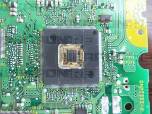
We can Attack Microcontroller AT88SC0104C Software, please view below Microcontroller AT88SC0104C features for your reference:
One of a family of nine devices with user memories from 1Kbit to 256Kbit
1Kbit (128-byte) EEPROM user memory
Four 32 byte (256 bit) zones
Self-timed write cycle
Single byte or 16-byte page write mode
Programmable access rights for each zone when Attack Microcontroller
2Kbit configuration zone
· 37-byte OTP area for user-defined codes
· 160-byte area for user-defined keys and passwords
High security features
64-bit mutual authentication protocol (under license of ELVA) when Attack Microcontroller
Encrypted checksum
Stream encryption
Four key sets for authentication and encryption
Eight sets of two 24-bit passwords
Anti-tearing function
Voltage and frequency monitor if Attack Microcontroller
Smart card features
ISO 7816 Class A (5V) or Class B (3V) operation
ISO 7816-3 asynchronous T = 0 protocol (Gemplus® patent) *
Multiple zones, key sets and passwords for multi-application use
Synchronous two-wire serial interface for faster device initialization * before Attack Microcontroller
Programmable 8-byte answer-to-reset register
ISO 7816-2 compliant modules
Embedded application features
Low voltage operation: 2.7V to 5.5V after Attack Microcontroller
Secure nonvolatile storage for sensitive system or user information
Two-wire serial interface
1.0MHz compatibility for fast operation
Standard 8-lead plastic packages, green compliant (exceeds RoHS) when Attack Microcontroller
Same pinout as two-wire Serial EEPROM’s
High reliability if REVERSE ENGINEERING Microcontroller
· Endurance: 100,000 cycles
· Data retention: 10 years
· ESD protection: 4,000V min
 Posted in Recover MCU |
  Tags: kopieren integrierte Schaltung bin, kopieren integrierte Schaltung code, kopieren integrierte Schaltung data, kopieren integrierte Schaltung eeprom, kopieren integrierte Schaltung hex, kopieren integrierte Schaltung memory, kopieren integrierte Schaltung program |
  Comments Closed
Decap IC PIC16C55 Eeprom
Decap IC PIC16C55 Eeprom and extract mcu pic16c55 heximal from flash memory, and clone firmware to new microcontroller pic16c55 to provide the same functions;
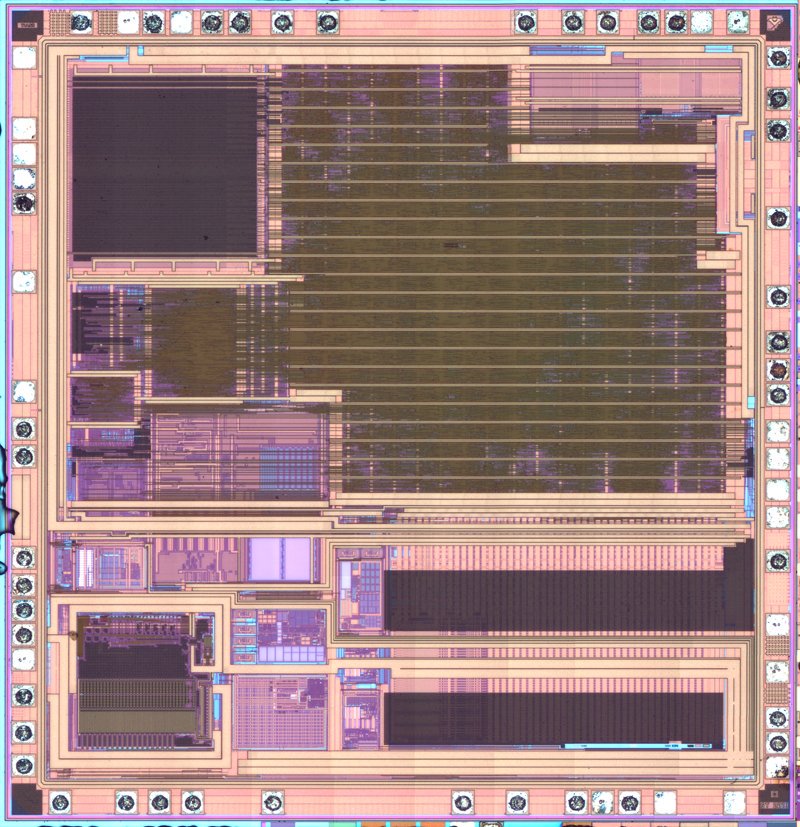
Setting both UMSELn1:0 bits to one enables the USART in MSPIM logic. In this mode of operation the SPI master control logic takes direct control over the USART resources.
These resources include the transmitter and receiver shift register and buffers, and the baud rate generator. The parity generator and checker, the data and clock recovery logic, and the RX and TX control logic is disabled if recover mcu pic16f873 hex.
The USART RX and TX control logic is replaced by a common SPI transfer control logic. However, the pin control logic and interrupt generation logic is identical in both modes of operation.
The I/O register locations are the same in both modes. However, some of the functionality of the control registers changes when using MSPIM before recover mcu dspic30f6013 firmware.
The Clock Generation logic generates the base clock for the Transmitter and Receiver. For USART MSPIM mode of operation only internal clock generation (i.e. master operation) is supported.
The Data Direction Register for the XCKn pin (DDR_XCKn) must therefore be set to one (i.e. as output) for the USART in MSPIM to operate correctly when break mcu at89c5131a IC.
Preferably the DDR_XCKn should be set up before the USART in MSPIM is enabled (i.e. TXENn and RXENn bit set to one). The internal clock generation used in MSPIM mode is identical to the USART synchronous master mode.
The baud rate or UBRRn setting can therefore be calculated using the same equations, see Table 110: Table 110. Equations for Calculating Baud Rate Register Setting There are four combinations of XCKn (SCK) phase and polarity with respect to serial data, which are determined by control bits UCPHAn and UCPOLn.
The data transfer timing diagrams are shown in Figure 90. Data bits are shifted out and latched in on opposite edges of the XCKn signal, ensuring sufficient time for data signals to stabilize.
The UCPOLn and UCPHAn functionality is summarized in Table 111. Note that changing the setting of any of these bits will corrupt all ongoing communication for both the Receiver and Transmitter.
Posted in Recover MCU |
Tags: decap ic bin, decap ic code, decap ic data, decap ic eeprom, decap ic file, decap ic firmware, decap ic fuse bits, decap ic hex, decap ic memory, decap ic security bits, decap ic software |
Comments Closed
Decap IC PIC16C54A Heximal file
Decap IC PIC16C54A and clone microcomputer pic16c54a memory content, and read mcu pic16c54a Heximal file out from its flash and eeprom memory;
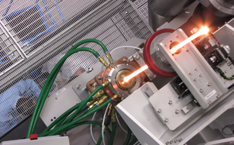
Bit 4 – RXENn: Receiver Enable n
Writing this bit to one enables the USART Receiver. The Receiver will override normal port operation for the RxDn pin when enabled. Disabling the Receiver will flush the receive buffer invalidating the FEn, DORn, and UPEn Flags when copy microcontroller at89c51re2 bin file.
Bit 3 – TXENn: Transmitter Enable n
Writing this bit to one enables the USART Transmitter. The Transmitter will override normal port operation for the TxDn pin when enabled.
The disabling of the Transmitter (writing TXENn to zero) will not become effective until ongoing and pending transmissions are completed, i.e., when the Transmit Shift Register and Transmit Buffer Register do not contain data to be transmitted. When disabled, the Transmitter will no longer override the TxDn port.
Bit 2 – UCSZn2: Character Size n
The UCSZn2 bits combined with the UCSZn1:0 bit in UCSRnC sets the number of data bits (Character SiZe) in a frame the Receiver and Transmitter use after recover IC c8051f340 hex file.
Bit 1 – RXB8n: Receive Data Bit 8 n
RXB8n is the ninth data bit of the received character when operating with serial frames with nine data bits. Must be decap before decaping the low bits from UDRn when break IC STM32F101C4T6 hex file.
Bit 0 – TXB8n: Transmit Data Bit 8 n
TXB8n is the ninth data bit in the character to be transmitted when operating with serial frames with nine data bits. Must be written before writing the low bits to UDRn.
Bits 7:6 – UMSELn1:0 USART Mode Select
These bits select the mode of operation of the USARTn as shown in Table 101..
Bits 5:4 – UPMn1:0: Parity Mode
These bits enable and set type of parity generation and check. If enabled, the Transmitter will automatically generate and send the parity of the transmitted data bits within each frame.
The Receiver will generate a parity value for the incoming data and compare it to the UPMn setting. If a mismatch is detected, the UPEn Flag in UCSRnA will be set.
Bit 3 – USBSn: Stop Bit Select
This bit selects the number of stop bits to be inserted by the Transmitter. The Receiver ignores this setting.
Posted in Recover MCU |
Tags: decap ic bin, decap ic code, decap ic content, decap ic data, decap ic eeprom, decap ic file, decap ic firmware, decap ic flash, decap ic hex, decap ic lock bit, decap ic memory, decap ic program, decap ic software |
Comments Closed
Reverse Engineering Chip PIC12C508 Code
Reverse Engineering Chip PIC12C508 Code need to extract the embedded firmware from locked microcontroller pic12c508, then crack mcu protective system;
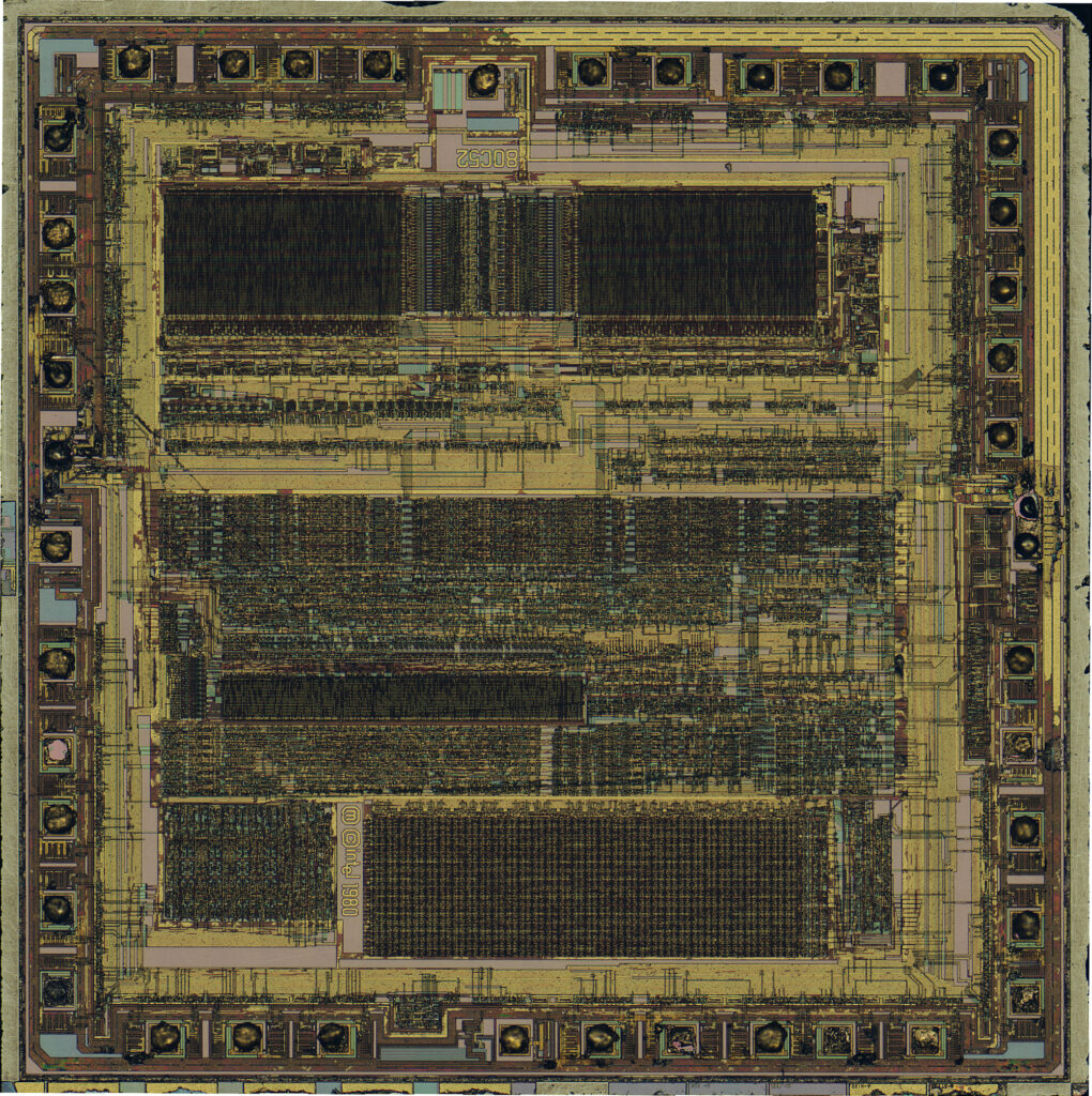
The recommendations of the maximum receiver baud rate error was made under the assumption that the Receiver and Transmitter equally divides the maximum total error. There are two possible sources for the receivers baud rate error. The Receiver’s system clock (XTAL) will always have some minor instability over the supply voltage range and the temperature range.
When using a crystal to generate the system clock, this is rarely a problem, but for a resonator the system clock may differ more than 2% depending of the resonators tolerance. The second source for the error is more controllable. The baud rate generator can not always do an exact division of the system frequency to get the baud rate wanted after copy mcu pic16f870 program.
In this case an UBRR value that gives an acceptable low error can be used if possible. Setting the Multi-processor Communication mode (MPCMn) bit in UCSRnA enables a filtering function of incoming frames received by the USART Receiver.
Frames that do not contain address information will be ignored and not put into the receive buffer. This effectively reduces the number of incoming frames that has to be handled by the CPU, in a system with multiple CHIPs that communicate via the same serial bus if attacking mcu c8051f530 firmware.
The Transmitter is unaffected by the MPCMn setting, but has to be used differently when it is a part of a system utilizing the Multi-processor Communication mode. If the Receiver is set up to receive frames that contain 5 to 8 data bits, then the first stop bit indicates if the frame contains data or address information. If the Receiver is set up for frames with nine data bits, then the ninth bit (RXB8n) is used for identifying address and data frames.
When the frame type bit (the first stop or the ninth bit) is one, the frame contains an address. When the frame type bit is zero the frame is a data frame.
The Multi-processor Communication mode enables several slave CHIPs to receive data from a master CHIP. This is done by first decoding an address frame to find out which CHIP has been addressed if attack microcontroller pic16c63a hex.
If a particular slave CHIP has been addressed, it will receive the following data frames as normal, while the other slave CHIPs will ignore the received frames until another address frame is received.
Posted in Recover MCU |
Tags: reverse engineering chip archive, reverse engineering chip bin, reverse engineering chip code, reverse engineering chip content, reverse engineering chip data, reverse engineering chip eeprom, reverse engineering chip file, reverse engineering chip firmware, reverse engineering chip hex, reverse engineering chip information, reverse engineering chip memory, reverse engineering chip program |
Comments Closed
Reverse Microcontroller PIC12C508A Firmware
Reverse Microcontroller PIC12C508A structure and extract code from embedded mcu pic12c508a flash memory, decrypt the Firmware of pic12c508a microprocessor;
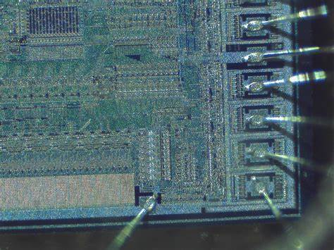
The clock recovery logic synchronizes internal clock to the incoming serial frames. Figure 87 illustrates the sampling process of the start bit of an incoming frame.
The sample rate is 16 times the baud rate for Normal mode, and eight times the baud rate for Double Speed mode. The horizontal arrows illustrate the synchronization variation due to the sampling process. Note the larger time variation when using the Double Speed mode (U2Xn = 1) of operation. Samples denoted zero are samples done when the RxDn line is idle (i.e., no communication activity).
Please shown in the figure. The clock recovery logic then uses samples 8, 9, and 10 for Normal mode, and samples 4, 5, and 6 for Double Speed mode (indicated with sample numbers inside boxes on the figure), to decide if a valid start bit is received.
If two or more of these three samples have logical high levels (the majority wins), the start bit is rejected as a noise spike and the Receiver starts looking for the next high to low-transition.
If however, a valid start bit is detected, the clock recovery logic is synchronized and the data recovery can begin. The synchronization process is repeated for each start bit before Breaking IC.
When the receiver clock is synchronized to the start bit, the data recovery can begin. The data recovery unit uses a state machine that has 16 states for each bit in Normal mode and eight states for each bit in Double Speed mode.
Figure 88 shows the sampling of the data bits and the parity bit. Each of the samples is given a number that is equal to the state of the recovery unit.The decision of the logic level of the received bit is taken by doing a majority voting of the logic value to the three samples in the center of the received bit when Restore IC program.
The center samples are emphasized on the figure by having the sample number inside boxes. The majority voting process is done as follows: If two or all three samples have high levels, the received bit is registered to be a logic 1.
If two or all three samples have low levels, the received bit is registered to be a logic 0. This majority voting process acts as a low pass filter for the incoming signal on the RxDn pin.
The recovery process is then repeated until a complete frame is received. Including the first stop bit. Note that the Receiver only uses the first stop bit of a frame.
Posted in Recover MCU |
Tags: reverse microcontroller archive, reverse microcontroller bin, reverse microcontroller code, reverse microcontroller content, reverse microcontroller data, reverse microcontroller eeprom, reverse microcontroller file, reverse microcontroller firmware, reverse microcontroller hex, reverse microcontroller information, reverse microcontroller memory, reverse microcontroller program |
Comments Closed
Reverse IC ATmega162P Eeprom
Reverse IC ATmega162P Eeprom after crack microcontroller atmega162p protective system, and extract locked code from mcu atmega162p flash memory;
Internal clock generation is used for the asynchronous and the synchronous master modes of operation. The description in this section refers to Figure 84. The USART Baud Rate Register (UBRRn) and the down-counter connected to it function as a programmable prescaler or baud rate generator.
The down-counter, running at system clock (fosc), is loaded with the UBRRn value each time the counter has counted down to zero or when the UBRRLn Register is written. A clock is generated each time the counter reaches zero. This clock is the baud rate generator clock output (= fosc/(UBRRn+1)). The Transmitter divides the baud rate generator clock output by 2, 8 or 16 depending on mode. The baud rate generator output is used directly by the Receiver’s clock and data recovery units after Reverse IC eeprom.
However, the recovery units use a state machine that uses 2, 8 or 16 states depending on mode set by the state of the UMSELn, U2Xn and DDR_XCKn bits. Table 98 contains equations for calculating the baud rate (in bits per second) and for calculating the UBRRn value for each mode of operation using an internally generated clock source after reverse Ic eeprom.
The transfer rate can be doubled by setting the U2Xn bit in UCSRnA. Setting this bit only has effect for the asynchronous operation. Set this bit to zero when using synchronous operation if reverse ic eeprom.
Setting this bit will reduce the divisor of the baud rate divider from 16 to 8, effectively doubling the transfer rate for asynchronous communication. Note however that the Receiver will in this case only use half the number of samples (reduced from 16 to 8) for data sampling and clock recovery, and therefore a more accurate baud rate setting and system clock are required when this mode is used. For the Transmitter, there are no downsides after Reverse IC eeprom.
External clocking is used by the synchronous slave modes of operation. The description in this section refers to Figure 84 for details. External clock input from the XCKn pin is sampled by a synchronization register to minimize the chance of meta-stability. The output from the synchronization register must then pass through an edge detector before it can be used by the Transmitter and Receiver when Reverse IC eeprom.
This process introduces a two CPU clock period delay and therefore the maximum external XCKn clock frequency is limited by the following equation when Reverse IC eeprom:
Note that fosc depends on the stability of the system clock source. It is therefore recommended to add some margin to avoid possible loss of data due to frequency variations.
When synchronous mode is used (UMSELn = 1), the XCKn pin will be used as either clock input (Slave) or clock output (Master). The dependency between the clock edges and data sampling or data change is the same. The basic principle is that data input (on RxDn) is sampled at the opposite XCKn clock edge of the edge the data output (TxDn) is changed when Reverse IC eeprom.
Posted in Recover MCU |
Tags: reverse ic archive, reverse ic bin, reverse ic code, reverse ic content, reverse ic data, reverse ic file, reverse ic firmware, reverse ic hex, reverse ic information, reverse ic memory, reverse ic program |
Comments Closed
Recover MCU PIC16F628 Firmware
Recover MCU PIC16F628 Firmware needs to unlock microcontroller pic16f628 protective memory and then readout embedded firmware from mcu pic16f628 flash memory;
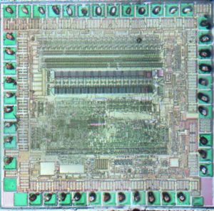
We can Recover MCU PIC16F628 Firmware, please view the MCU PIC16F628 features for your reference:
The PIC16F62X are 18-Pin FLASH-based members of the versatile PIC16CXX family of low-cost, high-performance, CMOS, fully-static, 8-bit microcontrollers. All PICmicro® microcontrollers employ an advanced RISC architecture.
The PIC16F62X have enhanced core features, eight-level deep stack, and multiple internal and external interrupt sources. The separate instruction and data buses of the Harvard architecture allow a 14-bit wide instruction word with the separate 8-bit wide data.
The two-stage instruction pipeline allows all instructions to execute in a single-cycle, except for program branches (which require two cycles). A total of 35 instructions (reduced instruction set) are available. Additionally, a large register set gives some of the architectural innovations used to achieve a very high performance.
PIC16F62X microcontrollers typically achieve a 2:1 code compression and a 4:1 speed improvement over other 8-bit microcontrollers in their class. PIC16F62X devices have special features to reduce external components, thus reducing system cost, enhancing system reliability and reducing power consumption.
There are eight oscillator configurations, of which the single pin ER oscillator provides a low-cost solution. The LP oscillator minimizes power consumption, XT is a standard crystal, INTRC is a self-contained internal oscillator and the HS is for High Speed crystals.
The SLEEP (power-down) mode offers power savings. The user can wake up the chip from SLEEP through several external and internal interrupts and reset.
A highly reliable Watchdog Timer with its own on-chip RC oscillator provides protection against software lock- up.
Table 1-1 shows the features of the PIC16F62X mid-range microcontroller families. A simplified block diagram of the PIC16F62X is shown in Figure 3-1.
The PIC16F62X series fits in applications ranging from battery chargers to low-power remote sensors. The FLASH technology makes customization of application programs (detection levels, pulse generation, timers, etc.) extremely fast and convenient.
The small footprint packages make this microcontroller series ideal for all applications with space limitations. Low-cost, low-power, high-performance, ease of use and I/O flexibility make the PIC16F62X very versatile.
The PIC16F62X family is supported by a full-featured macro assembler, a software simulator, an in-circuit emulator, a low-cost development programmer and a full-featured programmer. A Third Party “C” compiler support tool is also available.
Reverse Microcontroller ATmega8P Archive
Reverse Microcontroller ATmega8P Archive needs to crack mcu atmega8p protective system and then extract locked code from mcu atmega8p flash memory;
The dashed boxes in the block diagram separate the three main parts of the USART (listed from the top): Clock Generator, Transmitter and Receiver.
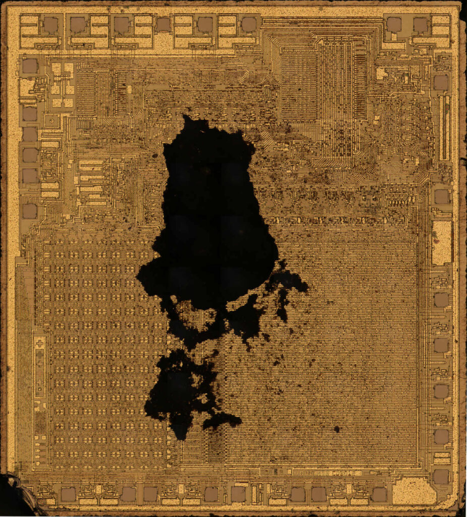
Control Registers are shared by all units. The Clock Generation logic consists of synchronization logic for external clock input used by synchronous slave operation, and the baud rate generator if Recover atmega164pa MCU code.
The XCKn (Transfer Clock) pin is only used by synchronous transfer mode. The Transmitter consists of a single write buffer, a serial Shift Register, Parity Generator and Control logic for handling different serial frame formats.
The write buffer allows a continuous transfer of data without any delay between frames. The Receiver is the most complex part of the USART module due to its clock and data recovery units.
The recovery units are used for asynchronous data reception. In addition to the recovery units, the Receiver includes a Parity Checker, Control logic, a Shift Register and a two level receive buffer (UDRn).
The Receiver supports the same frame formats as the Transmitter, and can detect Frame Error, Data OverRun and Parity Errors if break microcontroller atmega324a binary.
The Clock Generation logic generates the base clock for the Transmitter and Receiver. The USARTn supports four modes of clock operation: Normal asynchronous, Double Speed asynchronous, Master synchronous and Slave synchronous mode.
The UMSELn bit in USART Control and Status Register C (UCSRnC) selects between asynchronous and synchronous operation. Double Speed (asynchronous mode only) is controlled by the U2Xn found in the UCSRnA Register.
When using synchronous mode (UMSELn = 1), the Data Direction Register for the XCKn pin (DDR_XCKn) controls whether the clock source is internal (Master mode) or external (Slave mode). The XCKn pin is only active when using synchronous mode.
Posted in Recover MCU |
Tags: reverse microcontroller archive, reverse microcontroller bin, reverse microcontroller code, reverse microcontroller content, reverse microcontroller data, reverse microcontroller eeprom, reverse microcontroller file, reverse microcontroller firmware, reverse microcontroller hex, reverse microcontroller information, reverse microcontroller memory, reverse microcontroller program |
Comments Closed