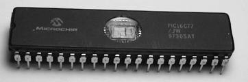
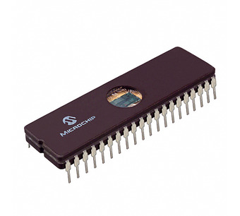
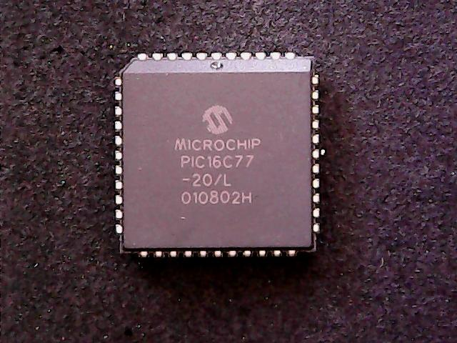
 Recover Chip PIC16C77 Code
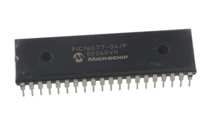
The PIC16C77 stands as a robust pillar in the world of 8-bit embedded control, specifically engineered for high-end applications requiring extensive I/O and sophisticated timing functions. This versatile MCU is a critical component in various high-stakes industries, including aerospace instrumentation, heavy industrial robotics, and advanced telecommunication switching systems. Its unique features—such as a large memory space for its era and high-speed execution—make it indispensable for managing complex data streams and real-time control algorithms. However, because these chips often utilize protective security bits to keep the internal firmware locked, many organizations find themselves in a precarious position when a device fails or the original source code is lost, leaving the secured logic unreachable through conventional means.
Our high-tech laboratory provides a specialized pathway to break through these hardware-level barriers and retrieve the essential binary archive that keeps your systems operational. To successfully attack a secured MCU, our specialists often use advanced physical techniques to decapsulate the silicon die, allowing for a precise micro-analysis of the protected logic gates. This method enables us to decode the heximal data directly from the internal flash or eeprom layers without destroying the underlying intelligence. Whether the goal is to clone a legacy controller to prevent factory downtime or duplicate the program from an encrypted chip for security auditing, our service provides the technical bridge to hack the limitations of embedded silicon. By focusing on the PIC16C77 architecture, we ensure that every locked file or program is recovered with surgical accuracy, transforming a “black box” back into a usable source code asset.
There are actually two 8-bit latches, one for data-out (from the PIC16/17) and one for data input. The user writes 8-bit data to PORTD data latch and reads data, Chip Select from the port pin latch (note that they have the same address). In this mode, the TRISD register is ignored, since the microprocessor is controlling the direction of A write to the PSP occurs when both the CS and WR lines are first detected low. When either the CS or WR lines become high (level triggered), then the Input Buffer Full status flag bit IBF (TRISE<7>) is set on the Q4 clock cycle, following the next Q2 cycle, to signal the write is complete (Figure 5-12). The interrupt flag bit PSPIF (PIR1<7>) is also set on the same Q4 clock cycle. IBF can only be cleared by reading the PORTD input latch. The input Buffer Overflow status flag bit IBOV (TRISE<5>) is set if a second write to the Parallel Slave Port is attempted when the previous byte has not been read out of the buffer.
A read from the PSP occurs when both the CS and RD lines are first detected low. The Output Buffer Full status flag bit OBF (TRISE<6>) is cleared immediately (Figure 5-13) indicating that the PORTD latch is waiting to be read by the external bus before Recover Chip PIC16C77 Code.
When either the CS or RD pin becomes high (level triggered), the interrupt flag bit PSPIF is set on the Q4 clock cycle, following the next Q2 cycle, indicating that the read is complete. OBF remains low until data is written to PORTD by the user firmware.
When not in Parallel Slave Port mode, the IBF and OBF bits are held clear. However, if flag bit IBOV was previously set, it must be cleared in firmware. An interrupt is generated and latched into flag bit PSPIF when a read or write operation is completed. PSPIF must be cleared by the user in firmware and the interrupt can be disabled by clearing the interrupt enable bit PSPIE (PIE1<7>).
The Timer0 module is a simple 8-bit overflow counter.
The clock source can be either the internal system clock (Fosc/4) or an external clock. When the clock CCP Overview source is an external clock, the Timer0 module can be selected to increment on either the rising or falling edge.
The Timer0 module also has a programmable prescaler option. This prescaler can be assigned to either the Timer0 module or the Watchdog Timer. Bit PSA (OPTION<3>) assigns the prescaler, and bits PS2:PS0 (OPTION<2:0>) determine the prescaler value. Timer0 can increment at the following rates: 1:1 (when pres-caler assigned to Watchdog timer), 1:2, 1:4, 1:8, 1:16, 1:32, 1:64, 1:128, and 1:256 (Timer0 only) if Recover Chip PIC16C77 Code.
Synchronization of the external clock occurs after the prescaler. When the prescaler is used, the external clock frequency may be higher then the device’s frequency. The maximum frequency is 50 MHz, given the high and low time requirements of the clock Timer1 is a 16-bit timer/counter.
The clock source can be either the internal system clock (Fosc/4), an external clock, or an external crystal. Timer1 can operate as either a timer or a counter. When operating as a counter (external clock source) when Recover Chip, the counter can either operate synchronized to the device or asynchronously to the device. Asynchronous operation allows Timer1 to operate during sleep, which is useful for applications that require a real-time clock as well as the power savings of SLEEP mode.
Timer1 also has a prescaler option which allows Timer1 to increment at the following rates: 1:1, 1:2, 1:4, and 1:8. Timer1 can be used in conjunction with the Capture/Compare/PWM module. When used with a CCP module, Timer1 is the time-base for 16-bit Capture or the 16-bit Compare and must be synchronized to the device after Recover Chip PIC16C77 Code.
The CCP module(s) can operate in one of these three modes: 16-bit capture, 16-bit compare, or up to 10-bit Pulse Width Modulation (PWM). Capture mode captures the 16-bit value of TMR1 into the CCPRxH:CCPRxL register pair. The capture event can be programmed for either the falling edge, rising edge, fourth rising edge, or the sixteenth rising edge of the CCPx pin.
The fundamental purpose of performing a targeted attack to break the security of a protected PIC16C77 is to ensure the continuity of critical infrastructure that would otherwise face forced obsolescence. For many end users, the ability to retrieve a heximal archive from a locked MCU is a strategic necessity that avoids the massive costs associated with a total system redesign. By choosing to decode or hack the secured internal memory, our clients can successfully clone or duplicate their vital firmware onto fresh hardware. This ensures that the binary data remains a functional asset even when the original manufacturer no longer supports the part. Our expertise allows you to duplicate the flash and eeprom contents of any embedded controller, ensuring that your protected logic is preserved for the long term.
Ultimately, our recovery service grants the end user total control over their proprietary technology and hardware lifecycle. Instead of struggling with the impossible task of rewriting ancient source code, you can simply retrieve the heximal file and clone the locked program directly onto a replacement MCU. We specialize in the precision required to decapsulate and attack these high-security chips, ensuring that the binary data is handled with the highest level of integrity. By providing a reliable way to decode and duplicate the firmware of a secured PIC16C77, we turn a protected archive into a living part of your current operations. Our commitment is to ensure that your data, memory, and program files remain accessible, regardless of the protective measures originally placed upon the silicon, giving you the freedom to maintain your equipment on your own terms.