Archive for August, 2014
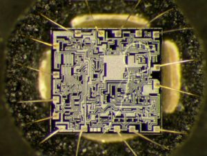
 Break Microcontroller PIC16C716 Heximal
There are two memory blocks in each of these PICmicro® microcontroller devices. Each block (Program Memory and Data Memory) has its own bus so that concurrent access can occur which provide necessity for Break Microcontroller PIC16C716 Heximal.
The PIC16C712/716 has a 13-bit program counter capable of addressing an 8K x 14 program memory space. PIC16C712 has 1K x 14 words of program memory and PIC16C716 has 2K x 14 words of program memory. Accessing a location above the physically implemented address will cause a wraparound.

Break Microcontroller PIC16C716 Heximal
The reset vector is at 0000h and the interrupt vector is at 0004h.
Each bank extends up to 7Fh (128 bytes). The lower locations of each bank are reserved for the Special
Function Registers. Above the Special Function Registers are General Purpose Registers, implemented as static RAM. All implemented banks contain special function registers. Some “high use” special function registers from one bank may be mirrored in another bank for code reduction and quicker access.
The Special Function Registers are registers used by the CPU and Peripheral Modules for controlling the desired operation of the device.
The special function registers can be classified into two sets; core (CPU) and peripheral. Those registers associated with the core functions are described in detail in this section. Those related to the operation of the peripheral features are described in detail in that peripheral feature section.
The STATUS register, shown in Figure 2-4, contains the arithmetic status of the ALU, the RESET status and the bank select bits for data memory in the process of Break Microcontroller PIC16C716 Heximal. The STATUS register can be the destination for any instruction, as with any other register.
If the STATUS register is the destination for an instruction that affects the Z, DC or C bits, then the write to these three bits is disabled. These bits are set or cleared according to the device logic. Furthermore, the TO and PD bits are not writable. Therefore, the result of an instruction with the STATUS register as destination may be different than intended.
The program counter (PC) specifies the address of the instruction to fetch for execution. The PC is 13 bits wide. The low byte is called the PCL register after Break Microcontroller. This register is readable and writable. The high byte is called the PCH register. This register contains the PC<12:8> bits and is not directly readable or writable. All updates to the PCH register go through the PCLATH register.
The stack allows a combination of up to 8 program calls and interrupts to occur. The stack contains the return address from this branch in program execution. Midrange devices have an 8 level deep x 13-bit wide hardware stack. The stack space is not part of either program or data space and the stack pointer is not readable or writable. The PC is PUSHed onto the stack when a CALL instruction is executed or an interrupt causes a branch. The stack is POPed in the event of a RETURN, RETLW or a RETFIE instruction execution.
PCLATH is not modified when the stack is PUSHed or POPed.
After the stack has been PUSHed eight times, the ninth push overwrites the value that was stored from the first push. The tenth push overwrites the second push (and so on).
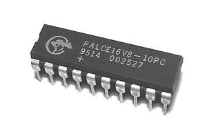
Break Chip PALCE16V8 Software
The Cypress PALCE16V8 is a CMOS Flash Electrical Erasable second-generation programmable array logic device. It is implemented with the familiar sum-of-product (AND-OR) logic structure and the programmable macrocell which is easier to Break Chip PALCE16V8 Software.
Functional Description (continued)
The PALCE16V8 is executed in a 20-pin 300-mil molded DIP, a 300-mil cerdip, a 20-lead square ceramic leadless chip car-
rier, and a 20-lead square plastic leaded chip carrier. The device provides up to 16 inputs and 8 outputs. The PALCE16V8 can be electrically erased and reprogrammed. The programmable macrocell enables the device to function as a superset to the familiar 20-pin PLDs such as 16L8, 16R8, 16R6, and 16R4.
The PALCE16V8 features 8 product terms per output and 32 input terms into the AND array. The first product term in a macrocell can be used either as an internal output enable control or as a data product term.
Break Chip PALCE16V8 Software
There are a total of 18 architecture bits in the PALCE16V8 macrocell; two are global bits that apply to all macrocells and 16 that apply locally, two bits per macrocell.
The architecture bits determine whether the macrocell functions as a register or combinatorial with inverting or noninverting output. The output enable control can come from an external pin or internally from a product term.
The output can also be permanently enabled, functioning as a dedicated output or permanently disabled, functioning as a dedicated input. Feedback paths are selectable from either the input/output pin associated with the macrocell, the input/output pin associated with an adjacent pin, or from the macrocell register itself to Break Chip PALCE16V8 Software.
Configuration Table
Power-Up Reset
All registers in the PALCE16V8 power-up to a logic LOW for predictable system initialization. For each register, the associated output pin will be HIGH due to active-LOW outputs.
Electronic Signature
An electronic signature word is provided in the PALCE16V8 that consists of 64 bits of programmable memory that can contain user-defined data.
Security Bit
A security bit is provided that defeats the readback of the internal programmed pattern when the bit is programmed.
Low Power
Product Term Disable
Product Term Disable (PTD) fuses are included for each product term. The PTD fuses allow each product term to be individually disabled.
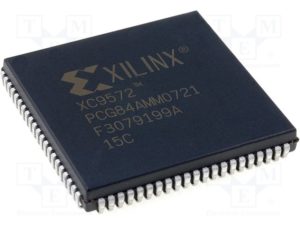
Break IC XC9572-15PQ100C Binary
We can Break IC XC9572-15PQ100C Binary, below IC XC9572-15PQ100C features for your reference:
Features
7.5 ns pin-to-pin logic delays on all pins fCNT to 125 MHz
72 macrocells with 1,600 usable gates
Up to 72 user I/O pins
5V in-system programmable
Product Specification
Description
The XC9572 is a high-performance CPLD providing advanced in-system programming and test capabilities for general purpose logic integration which is one of the main reasons for its popularity of Break IC XC9572-15PQ100C Binary. It is comprised of eight 36V18 Function Blocks, providing 1,600 usable gates with propagation delays of 7.5 ns. See Figure 2 for the architecture overview.
Break IC XC9572-15PQ100C Binary
– Endurance of 10,000 program/erase cycles
– Program/erase over full commercial voltage and temperature range
Enhanced pin-locking architecture
Flexible 36V18 Function Block
– 90 product terms drive any or all of 18 macrocells within Function Block
– Global and product term clocks, output enables, set and reset signals
Extensive IEEE Std 1149.1 boundary-scan (JTAG) support
Programmable power reduction mode in each macrocell
Slew rate control on individual outputs
User programmable ground pin capability
Extended pattern security features for design protection
High-drive 24 mA outputs
3.3V or 5V I/O capability
Advanced CMOS 5V FastFLASH™ technology
Supports parallel programming of more than one
XC9500 concurrently
Available in 44-pin PLCC, 84-pin PLCC, 100-pin PQFP, and 100-pin TQFP packages
Power Management
Power dissipation can be reduced in the XC9572 by configuring macrocells to standard or low-power modes of operation. Unused macrocells are turned off to minimize power dissipation when Break IC XC9572-15PQ100C Binary.
ICC (mA) = MCHP (1.7) + MCLP (0.9) + MC (0.006 mA/MHz) f
Where:
MCHP = Macrocells in high-performance mode
MCLP = Macrocells in low-power mode
MC = Total number of macrocells used f = Clock frequency (MHz)
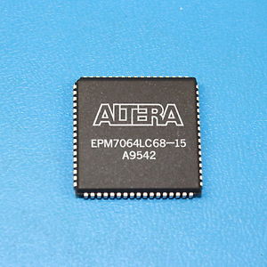
Break CPLD EPM7064LC68-15 Binary
We can Break CPLD EPM7064LC68-15 Binary, please view below CPLD EPM7064LC68-15 features for your reference:
Features
High-performance, EEPROM-based programmable logic devices (PLDs) based on second-generation MAX® architecture 5.0-V in-system programmability (ISP) through the built-in.
IEEE Std. 1149.1 Joint Test Action Group (JTAG) interface available in MAX 7000S devices
– ISP circuitry compatible with IEEE Std. 1532 before Break CPLD
Includes 5.0-V MAX 7000 devices and 5.0-V ISP-based MAX 7000S devices
Built-in JTAG boundary-scan test (BST) circuitry in MAX 7000S devices with 128 or more macrocells if Break CPLD
Complete EPLD family with logic densities ranging from 600 to 5,000 usable gates (see Tables 1 and 2) 5-ns pin-to-pin logic delays with up to 175.4-MHz counter frequencies (including interconnect) by Break CPLD EPM7064LC68-15 Binary.
Break CPLD EPM7064LC68-15 Binary
PCI-compliant devices available
Altera Corporation
DS-MAX7000-6.7
For information on in-system programmable 3.3-V MAX 7000A or 2.5-V
MAX 7000B devices, see the MAX 7000A Programmable Logic Device Family
Data Sheet or theMAX 7000B Programmable Logic Device Family Data Sheet.
Circuit Engineering Company Limited continues to be recognized as the Southern China Leader in Services for IC Break, MCU RECOVER, Chip Recover, Microcontroller Copy service. With the advancement of today’s modern circuit board technology, it is more important than ever to have specialists available to help you at a moment’s notice.
Our engineering and commercial teams collectively have a vast amount of electronic experience covering field include Consumer Electronics, Industrial Automation Electronics, Wireless Communication Electronics., etc. For more information please contact us through email.
Attack CPLD EPM7096QC100-10 Binary
We can Attack CPLD EPM7096QC100-10 Binary, please view CPLD EPM7096QC100-10 features for your reference:
High-performance, EEPROM-based programmable logic devices (PLDs) based on second-generation MAX® architecture 5.0-V in-system programmability (ISP) through the built-in IEEE Std. 1149.1 Joint Test Action Group (JTAG) interface available in MAX 7000S devices
– ISP circuitry compatible with IEEE Std. 1532
Includes 5.0-V MAX 7000 devices and 5.0-V ISP-based MAX 7000S devices
Built-in JTAG boundary-scan test (BST) circuitry in MAX 7000S devices with 128 or more macrocells
Complete EPLD family with logic densities ranging from 600 to 5,000 usable gates (see Tables 1 and 2) 5-ns pin-to-pin logic delays with up to 175.4-MHz counter frequencies (including interconnect) PCI-compliant devices available.
Open-drain output option in MAX 7000S devices
Programmable macrocell flipflops with individual clear, preset, clock, and clock enable controls
Programmable power-saving mode for a reduction of over 50% in each macrocell.
Configurable expander product-term distribution, allowing up to 32 product terms per macrocell 44 to 208 pins available in plastic J-lead chip carrier (PLCC), ceramic pin-grid array (PGA), plastic quad flat pack (PQFP), power quad flat pack (RQFP), and 1.0-mm thin quad flat pack (TQFP) packages.
Programmable security bit for protection of proprietary designs
– MultiVoltTM I/O interface operation, allowing devices to interface with 3.3-V or 5.0-V devices (MultiVolt I/O operation is not available in 44-pin packages) – Pin compatible with low-voltage MAX 7000A and MAX 7000B devices.
Enhanced features available in MAX 7000E and MAX 7000S devices
– Six pin- or logic-driven output enable signals
– Two global clock signals with optional inversion
– Enhanced interconnect resources for improved routability
– Fast input setup times provided by a dedicated path from I/O pin to macrocell registers
Attack CPLD EPM7096QC100-10 Binary
– Programmable output slew-rate control
Software design support and automatic place-and-route provided by
Altera’s development system for Windows-based PCs and Sun SPARCstation, and HP 9000 Series 700/800 workstations
Additional design entry and simulation support provided by EDIF 2 0 0 and 3 0 0 netlist files, library of parameterized modules (LPM), Verilog HDL, VHDL, and other interfaces to popular EDA tools from manufacturers such as Cadence, Exemplar Logic, Mentor Graphics, OrCAD, Synopsys, and VeriBest Programming support.
– Altera’s Master Programming Unit (MPU) and programming hardware from third-party manufacturers program all MAX 7000 devices
– The BitBlasterTM serial download cable, ByteBlasterMVTM parallel port download cable, and MasterBlasterTM serial/universal serial bus (USB) download cable program MAX 7000S devices.
Copy CPLD XC2C128_VQ100 Content
Copy CPLD XC2C128_VQ100 Content
We can Copy CPLD XC2C128_VQ100 Content, please view below CPLD XC2C128_VQ100 features for your reference:
Features
· Optimized for 1.8V systems
– Industry’s fastest low power CPLD
– Densities from 32 to 512 macrocells
· Industry’s best 0.18 micron CMOS CPLD
– Optimized architecture for effective logic synthesis by Copy CPLD XC2C128_VQ100 Content
– Multi-voltage I/O operation — 1.5V to 3.3V
· Advanced system features
– Fastest in system programming
· 1.8V ISP using IEEE 1532 (JTAG) interface
– On-The-Fly Reconfiguration (OTF)
– IEEE1149.1 JTAG Boundary Scan Test
– Optional Schmitt trigger input (per pin)
– Multiple I/O banks on all devices
– Unsurpassed low power management
– SSTL2_1,SSTL3_1, and HSTL_1 on 128 macrocell and denser devices
– Hot pluggable PLA architecture
– Superior pinout retention
– 100% product term routability across function block Wide package availability including fine pitch:
– Chip Scale Package (CSP) BGA, Fine Line BGA, TQFP, PQFP, VQFP, and QFN packages
Free software support for all densities using Xilinx® WebPACK™ tool Industry leading nonvolatile 0.18 micron CMOS
· DataGATE external signal control
– Flexible clocking modes
· Optional DualEDGE triggered registers
· Clock divider (÷ 2,4,6,8,10,12,14,16)
· CoolCLOCK
– Global signal options with macrocell control
· Multiple global clocks with phase selection per macrocell
· Multiple global output enables
· Global set/reset
– Abundant product term clocks, output enables and set/resets
– Efficient control term clocks, output enables and set/resets for each macrocell and shared across function blocks from Copy CPLD XC2C128_VQ100 Content
– Advanced design security
– Open-drain output option for Wired-OR and LED drive
– Optional bus-hold, 3-state or weak pullup on select I/O pins
– Optional configurable grounds on unused I/Os
– Mixed I/O voltages compatible with 1.5V, 1.8V, process
– Guaranteed 1,000 program/erase cycles
– Guaranteed 20 year data retention
Family Overview
Xilinx CoolRunner™-II CPLDs deliver the high speed and ease of use associated with the XC9500/XL/XV CPLD family with the extremely low power versatility of the XPLA3 family in a single MCU Recovery. This means that the exact same parts can be used for high-speed data communications.
computing systems and leading edge portable products, with the added benefit of In System Programming. Low power consumption and high-speed operation are combined into a single family that is easy to use and cost effective. Clocking techniques and other power saving features extend the users’ power budget. The design features are supported starting with Xilinx ISE® 4.1i WebPACK tool.
Attack PLD EPM7128ELC84-10 Binary
High-performance, EEPROM-based programmable logic devices (PLDs) based on second-generation MAX® architecture 5.0-V in-system programmability (ISP) through the built-in IEEE Std. 1149.1 which has provide convenience for Attack PLD EPM7128ELC84-10 Binary.
Includes 5.0-V MAX 7000 devices and 5.0-V ISP-based MAX 7000S devices
Built-in JTAG boundary-scan test (BST) circuitry in MAX 7000S devices with 128 or more macrocells
Complete EPLD family with logic densities ranging from 600 to 5,000 usable gates (see Tables 1 and 2) 5-ns pin-to-pin logic delays with up to 175.4-MHz counter frequencies (including interconnect)
Attack PLD EPM7128ELC84-10 Binary
PCI-compliant devices available
Open-drain output option in MAX 7000S devices
Programmable macrocell flipflops with individual clear, preset, clock, and clock enable controls
Programmable power-saving mode for a reduction of over 50% in each macrocell
Configurable expander product-term distribution, allowing up to 32 product terms per macrocell
44 to 208 pins available in plastic J-lead chip carrier (PLCC), ceramic pin-grid array (PGA), plastic quad flat pack (PQFP), power quad flat pack (RQFP), and 1.0-mm thin quad flat pack (TQFP) packages
Programmable security bit for protection of proprietary designs
3.3-V or 5.0-V operation
– MultiVoltTM I/O interface operation, allowing devices to interface with 3.3-V or 5.0-V devices after Attack PLD EPM7128ELC84-10 Binary (MultiVolt I/O operation is not available in 44-pin packages)
– Pin compatible with low-voltage MAX 7000A and MAX 7000B devices
Enhanced features available in MAX 7000E and MAX 7000S devices
– Six pin- or logic-driven output enable signals
– Two global clock signals with optional inversion
– Enhanced interconnect resources for improved routability
– Fast input setup times provided by a dedicated path from I/O pin to macrocell registers
– Programmable output slew-rate control
Software design support and automatic place-and-route provided by Altera’s development system for Windows-based PCs and Sun SPARCstation, and HP 9000 Series 700/800 workstations.
Additional design entry and simulation support provided by EDIF 2 0 0 and 3 0 0 netlist files, library of parameterized modules (LPM), Verilog HDL, VHDL, and other interfaces to popular EDA tools from manufacturers such as Cadence, Exemplar Logic, Mentor Graphics, OrCAD, Synopsys, and VeriBest.
Programming support
– Altera’s Master Programming Unit (MPU) and programming hardware from third-party manufacturers program all MAX 7000 devices
– The BitBlasterTM serial download cable, ByteBlasterMVTM parallel port download cable, and MasterBlasterTM serial/universal serial bus (USB) download cable program MAX 7000S devices
Break CPLD EPM3128ATC100-7 Software
Break CPLD EPM3128ATC100-7 Software
High–performance, low–cost CMOS EEPROM–based programmable logic devices (PLDs) built on a MAX® architecture 3.3-V in-system programmability (ISP) through the built–in IEEE Std. 1149.1 Joint Test Action Group (JTAG) interface with advanced pin-locking capability when Break CPLD EPM3128ATC100-7 Software.
– Enhanced ISP algorithm for faster programming
– ISP_Done bit to ensure complete programming
– Pull-up resistor on I/O pins during in–system programming
High–density PLDs ranging from 600 to 10,000 usable gates 4.5–ns pin–to–pin logic delays with counter frequencies of up to 227.3 MHz
MultiVoltTM I/O interface enabling the device core to run at 3.3 V, while I/O pins are compatible with 5.0–V, 3.3–V, and 2.5–V logic levels
Pin counts ranging from 44 to 256 in a variety of thin quad flat pack (TQFP), plastic quad flat pack (PQFP), plastic J–lead chip carrier (PLCC), and FineLine BGATM packages
Hot–socketing support
Programmable interconnect array (PIA) continuous routing structure for fast, predictable performance.
PCI compatible
Bus–friendly architecture including programmable slew–rate control
Open–drain output option
Programmable macrocell flipflops with individual clear, preset, clock, and clock enable controls
Programmable power–saving mode for a power reduction of over 50% in each macrocell
Configurable expander product–term distribution, allowing up to 32 product terms per macrocell
Programmable security bit for protection of proprietary designs which is necessary to be removed when Break CPLD EPM3128ATC100-7 Software
Enhanced architectural features, including:
– 6 or 10 pin– or logic–driven output enable signals
– Two global clock signals with optional inversion
– Enhanced interconnect resources for improved routability
– Programmable output slew–rate control
Software design support and automatic place–and–route provided by Altera’s development systems for Windows–based PCs and Sun SPARCstations, and HP 9000 Series 700/800 workstations
Additional design entry and simulation support provided by EDIF 2 0 0 and 3 0 0 netlist files, library of parameterized modules (LPM), Verilog HDL, VHDL, and other interfaces to popular EDA tools from third–party manufacturers such as Cadence, Exemplar Logic, Mentor Graphics, OrCAD, Synopsys, Synplicity, and VeriBest.
Programming support with the Altera master programming unit (MPU), MasterBlasterTM communications cable, ByteBlasterMVTM parallel port download cable, BitBlasterTM serial download cable as well as programming hardware from third–party manufacturers and any in–circuit tester that supports JamTM Standard Test and Programming Language (STAPL) Files (.jam), Jam STAPL Byte-Code Files (.jbc), or Serial Vector Format Files (.svf).
Copy CPLD EPM9320ARC208-10 Binary
High-performance CMOS EEPROM-based programmable logic devices (PLDs) built on third-generation Multiple Array MatriX (MAX®) architecture which is the main reason for requirement on Copy CPLD EPM9320ARC208-10 Binary.
Copy CPLD EPM9320ARC208-10 Binary
5.0-V in-system programmability (ISP) through built-in IEEE Std.
1149.1 Joint Test Action Group (JTAG) interface
Built-in JTAG boundary-scan test (BST) circuitry compliant with IEEE Std. 1149.1-1990
High-density erasable programmable logic device (EPLD) family ranging from 6,000 to 12,000 usable gates (see Table 1)
10-ns pin-to-pin logic delays with counter frequencies of up to 144 MHz
Fully compliant with the peripheral component interconnect Special Interest Group’s (PCI SIG) PCI Local Bus Specification, Revision 2.2
Dual-output macrocell for independent use of combinatorial and registered logic
FastTrack® Interconnect for fast, predictable interconnect delays
Input/output registers with clear and clock enable on all I/O pins
Programmable output slew-rate control to reduce switching noise
MultiVolt™ I/O interface operation, allowing devices to interface with 3.3-V and 5.0-V devices
Configurable expander product-term distribution allowing up to 32 product terms per macrocell
Programmable power-saving mode for more than 50% power reduction in each macrocell
Programmable macrocell flipflops with individual clear, preset, clock, and clock enable controls
Programmable security bit for protection of proprietary designs which must be disable when Copy CPLD EPM9320ARC208-10 Binary
Software design support and automatic place-and-route
Altera’s MAX+PLUS® II development system on Windows-based PCs as well as Sun SPARCstation, HP 9000 Series 700/800, and IBM RISC System/6000 workstations
Additional design entry and simulation support provided by EDIF 200 and 300 netlist files, library of parameterized modules (LPM), Verilog HDL, VHDL, and other interfaces to popular EDA tools from manufacturers such as Cadence, Exemplar Logic, Mentor Graphics, OrCAD, Synopsys, Synplicity, and VeriBest
Programming support with Altera’s Master Programming Unit (MPU), BitBlasterTM serial download cable, ByteBlasterTM parallel port download cable, and ByteBlasterMVTM parallel port download cable, as well as programming hardware from third-party manufacturers.
Offered in a variety of package options with 84 to 356 pins.