Archive for the ‘Break IC’ Category
 Break IC ATmega461 Eeprom
 April 25th, 2010 |
  Author:
 Break IC ATmega461 and read Eeprom data and flash program out from microcontroller atmega461, reprogramme heximal file into new atmega461 mcu for cloning,
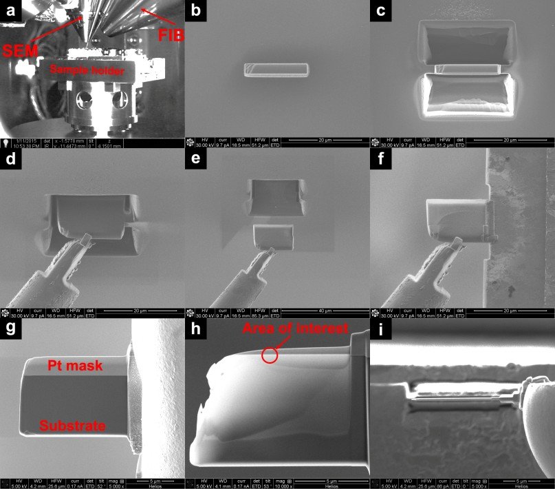
If Timer/Counter2 is used to wake the device up from Power-save or ADC Noise Reduction mode, precautions must be taken if the user wants to re-enter one of these modes: The interrupt logic needs one TOSC1 cycle to be reset when recover microcontroller pic18f252 program.
If the time between wake-up and re-entering sleep mode is less than one TOSC1 cycle, the interrupt will not occur, and the device will fail to wake up. If the user is in doubt whether the time before re-entering Power-save or ADC Noise Reduction mode is sufficient, the following algorithm can be used to ensure that one TOSC1 cycle has elapsed:
Write a value to TCCR2x, TCNT2, or OCR2x.
Wait until the corresponding Update Busy Flag in ASSR returns to zero.
Enter Power-save or ADC Noise Reduction mode before Break IC.When the asynchronous operation is selected, the 32.768 kHz Oscillator for Timer/Counter2 is always running, except in Power-down and Standby modes. After a Power-up Reset or wake-up from Power-down or Standby mode, the user should be aware of the fact that this Oscillator might take as long as one second to stabilize after recover microcontroller attiny13a hex.
The user is advised to wait for at least one second before using Timer/Counter2 after power-up or wake-up from Power-down or Standby mode and The contents of all Timer/Counter2 Registers must be considered lost after a wake-up from Power-down or Standby mode due to unstable clock signal upon start-up, no matter whether the Oscillator is in use or a clock signal is applied to the TOSC1 pin.
Description of wake up from Power-save or ADC Noise Reduction mode when the timer is clocked asynchronously: When the interrupt condition is met, the wake up process is started on the following cycle of the timer clock, that is, the timer is always advanced by at least one before the processor can break the counter value.
After wake-up, the MCU is halted for four cycles, it executes the interrupt routine, and resumes execution from the instruction following SLEEP.
Breaking of the TCNT2 Register shortly after wake-up from Power-save may give an incorrect result. Since TCNT2 is clocked on the asynchronous TOSC clock, breaking TCNT2 must be done through a register synchronized to the internal I/O clock domain.
Synchronization takes place for every rising TOSC1 edge. When waking up from Power-save mode, and the I/O clock (clkI/O) again becomes active, TCNT2 will break as the previous value (before entering sleep) until the next rising TOSC1 edge.
The phase of the TOSC clock after waking up from Power-save mode is essentially unpredictable, as it depends on the wake-up time. The recommended procedure for breaking TCNT2 is thus as follows:
Write any value to either of the registers OCR2x or TCCR2x.
Wait for the corresponding Update Busy Flag to be cleared.
During asynchronous operation, the synchronization of the Interrupt Flags for the asynchronous timer takes 3 processor cycles plus one timer cycle. The timer is therefore advanced by at least one before the processor can break the timer value causing the setting of the Interrupt Flag if Break IC eeprom.
The Output Compare pin is changed on the timer clock and is not synchronized to the processor clock.
Recovery Mcu PIC16F871 Software
Recovery Mcu PIC16F871 Software
We can Recovery Mcu PIC16F871 Software, please view the Mcu PIC16F871 features for your reference:
This document contains device-specific information.
Additional information may be found in the PICmicro™ Mid-Range Reference Manual, (DS33023), which may be obtained from your local Micromcu Sales Representative or downloaded from the Micromcu website. The Reference Manual should be considered a complementary document to this data sheet when Recovery Mcu, and is highly recommended reading for a better understanding of the device architecture and operation of the peripheral modules.
There are two devices (PIC16F870 and PIC16F871) covered by this data sheet. The PIC16F870 device comes in a 28-pin package and the PIC16F871 device comes in a 40-pin package. The 28-pin device does not have a Parallel Slave Port implemented. The following two figures are device block diagrams sorted by pin number; 28-pin for Figure 1-1 and 40-pin for Figure 1-2 if Recovery Mcu. The 28-pin and 40-pin pinouts are listed in Table 1-1 and Table 1-2, respectively.
There are three memory blocks in each of these PICmicro® MCUs. The Program Memory and Data Memory have separate buses, so that concurrent access can occur, and is detailed in this section. The EEPROM data memory block is detailed in Additional information on device memory may be found in the PICmicro Mid-Range Reference Manual, (DS33023) if recovery mcu.
The PIC16F870/871 devices have a 13-bit program counter capable of addressing an 8K x 14 program memory space. The PIC16F870/871 devices have 2K x 14 words of FLASH program memory. Accessing a location above the physically implemented address will cause a wraparound after Recovery Mcu.
The reset vector is at 0000h and the interrupt vector is at0004h The data memory is partitioned into multiple banks which contain the General Purpose Registers and the Special Function Registers. Bits RP1(STATUS<6>) and RP0 (STATUS<5>) are the bank select bits. Each bank extends up to 7Fh (128 bytes). The lower locations of each bank are reserved for the Special Function Registers when Recovery Mcu. Above the Special Function Registers are General Purpose Registers, implemented as static RAM. All implemented banks contain Special Function Registers. Some “high use” Special Function
Registers from one bank may be mirrored in another bank for code reduction and quicker access. The Special Function Registers are registers used by the CPU and peripheral modules for controlling the desired operation of the device. These registers are implemented as static RAM after Recovery Mcu.
Break MCU ATMEGA261PA Program
We can Break MCU ATMEGA261PA Program, please view the MCU ATMEGA261PA features for your reference:
When EXCLK is written to one, and asynchronous clock is selected, the external clock input buffer is enabled and an external clock can be input on Timer Oscillator 1 (TOSC1) pin instead of a 32 kHz crystal. Writing to EXCLK should be done before asynchronous operation is selected when Break MCU.
Note that the crystal Oscillator will only run when this bit is zero. When AS2 is written to zero, Timer/Counter2 is clocked from the I/O clock, clkI/O. When AS2 is written to one, Timer/Counter2 is clocked from a crystal Oscillator connected to the Timer Oscillator 1 (TOSC1) pin. When the value of AS2 is changed, the contents of TCNT2, OCR2A, OCR2B, TCCR2A and TCCR2B might be corrupted if Break MCU.
When Timer/Counter2 operates asynchronously and TCNT2 is written, this bit becomes set. When TCNT2 has been updated from the temporary storage register, this bit is cleared by hardware. A logical zero in this bit indicates that TCNT2 is ready to be updated with a new value if Break MCU.
When Timer/Counter2 operates asynchronously and OCR2A is written, this bit becomes set. When OCR2A has been updated from the temporary storage register, this bit is cleared by hardware. A logical zero in this bit indicates that OCR2A is ready to be updated with a new value before Break MCU.
When Timer/Counter2 operates asynchronously and OCR2B is written, this bit becomes set. When OCR2B has been updated from the temporary storage register, this bit is cleared by hardware. A logical zero in this bit indicates that OCR2B is ready to be updated with a new value after Break MCU.
When Timer/Counter2 operates asynchronously and TCCR2A is written, this bit becomes set. When TCCR2A has been updated from the temporary storage register, this bit is cleared by hardware. A logical zero in this bit indicates that TCCR2A is ready to be updated with a new value if Break MCU.
When Timer/Counter2 operates asynchronously and TCCR2B is written, this bit becomes set. When TCCR2B has been updated from the temporary storage register, this bit is cleared by hardware. A logical zero in this bit indicates that TCCR2B is ready to be updated with a new value when Break MCU.
 Posted in Break IC |
  Tags: break mcu archive, break mcu binary, break mcu code, break mcu content, break mcu data, break mcu eeprom, break mcu file, break mcu firmware, break mcu heximal, break mcu information, break mcu memory, break mcu program |
  Comments Closed
Break Mcu PIC16F870 Binary
We can Break Mcu PIC16F870 Binary, please view the Mcu PIC16F870 features for your reference:
Mcu Core Features:
· High-performance RISC CPU
· Only 35 single word instructions to learn
· All single cycle instructions except for program branches which are two cycle when Break Mcu
· Operating speed: DC – 20 MHz clock input DC – 200 ns instruction cycle
· 2K x 14 words of FLASH Program Memory
128 x 8 bytes of Data Memory (RAM)
64 x 8 bytes of EEPROM Data Memory
· Pinout compatible to the PIC16CXXX 28 and 40-pin devices if Break Mcu
· Interrupt capability (up to 11 sources)
· Eight level deep hardware stack
· Direct, indirect and relative addressing modes
· Power-on Reset (POR)
· Power-up Timer (PWRT) and
Oscillator Start-up Timer (OST)
· Watchdog Timer (WDT) with its own on-chip RC oscillator for reliable operation before Break Mcu
· Programmable code-protection
· Power saving SLEEP mode
· Selectable oscillator options
· Low-power, high-speed CMOS FLASH/EEPROM technology
· Fully static design
· In-Circuit Serial Programming (ICSP) via two pins
· Single 5V In-Circuit Serial Programming capability
· In-Circuit Debugging via two pins
· Processor read/write access to program memory
· Wide operating voltage range: 2.0V to 5.5V after Break Mcu
· High Sink/Source Current: 25 mA
· Commercial and Industrial temperature ranges
· Low-power consumption:
– < 1.6 mA typical @ 5V, 4 MHz
– 20 µA typical @ 3V, 32 kHz
– < 1 µA typical standby current
Peripheral Features:
· Timer0: 8-bit timer/counter with 8-bit prescaler
· Timer1: 16-bit timer/counter with prescaler, can be incremented during sleep via external crystal/clock
· Timer2: 8-bit timer/counter with 8-bit period register, prescaler and postscaler before Break Mcu
· One Capture, Compare, PWM module
– Capture is 16-bit, max. resolution is 12.5 ns
– Compare is 16-bit, max. resolution is 200 ns
– PWM max. resolution is 10-bit
· 10-bit multi-channel Analog-to-Digital converter
· Universal Synchronous Asynchronous Receiver Transmitter (USART/SCI) with 9-bit address detection
· Parallel Slave Port (PSP) 8-bits wide, with external RD, WR and CS controls (40/44-pin only) if Break Mcu
· Brown-out detection circuitry for Brown-out Reset (BOR)
Posted in Break IC |
Tags: mcu locked archive break, mcu locked code break, mcu locked dump break, mcu locked eeprom break, mcu locked firmware break, mcu locked information break, mcu locked memory break, mcu locked program break |
Comments Closed
Break IC PIC12F519 Binary
Break IC PIC12F519 Binary will begin from unlock microprocessor pic12f519 eeprom and flash memory, and then readout the secured code from mcu pic12f519;
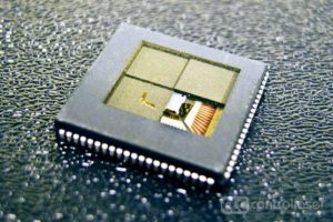
Break IC PIC12F519 Binary will begin from unlock microprocessor pic12f519 eeprom and flash memory, and then readout the secured code from mcu pic12f519
High-Performance RISC CPU:
· Only 33 Single-Word Instructions
· All Single-Cycle Instructions except for Program Branches which are Two-Cycle
· Two-Level Deep Hardware Stack
· Direct, Indirect and Relative Addressing modes for Data and Instructions
· Operating Speed:
– DC – 8 MHz Oscillator
– DC – 500 ns instruction cycle
· On-chip Flash Program Memory
– 1024 x 12
· General Purpose Registers (SRAM)
– 41 x 8
· Flash Data Memory
– 64 x 8
Special Microcontroller Features:
· 8 MHz Precision Internal Oscillator
– Factory calibrated to ±1%
· In-Circuit Serial Programming™ (ICSP™)
· In-Circuit Debugging (ICD) Support
· Power-on Reset (POR)
· Device Reset Timer (DRT)
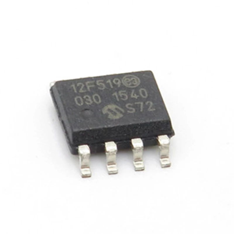
Extrair o microchip PIC12F519 seguro MCU Flash Code precisa quebrar o bit de fusível protegido IC pic12f519 protegido e, em seguida, extrair o arquivo heximal da memória flash do microcontrolador bloqueado pic12f519
· Watchdog Timer (WDT) with Dedicated On-Chip RC Oscillator for Reliable Operation
· Programmable Code Protection
· Multiplexed MCLR Input Pin
· Internal Weak Pull-ups on I/O Pins
· Power-Saving Sleep mode
· Wake-up from Sleep on Pin Change
· Selectable Oscillator Options:
– INTRC: 4 MHz or 8 MHz precision Internal RC oscillator
– EXTRC: External low-cost RC oscillator
– XT: Standard crystal/resonator
– LP: Power-saving, low-frequency crystal
Low-Power Features/CMOS Technology:
· Standby Current:
– 100 nA @ 2.0V, typical
· Operating Current:
– 11 ìA @ 32 kHz, 2.0V, typical
– 175 ìA @ 4 MHz, 2.0V, typical
· Watchdog Timer Current:
– 1 ìA @ 2.0V, typical
– 7 ìA @ 5.0V, typical
· High Endurance Program and Flash Data Memory Cells
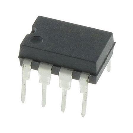
quebrar microcontrolador bloqueado PIC12F519 bit de fusível de segurança e leitura heximal embutido do microprocessador seguro pic12f519, programa binário original do clone para a nova unidade MCU pic12f519;
– 100,000 write Program Memory endurance
– 1,000,000 write Flash Data Memory endurance
– Program and Flash Data retention: >40 years
· Fully Static Design
· Wide Operating Voltage Range: 2.0V to 5.5V
– Wide temperature range
– Industrial: -40°C to +85°C
– Extended: -40°C to +125°C
Peripheral Features:
· 6 I/O Pins
– 5 I/O pins with individual direction control
– High current sink/source for direct LED drive
· 8-bit Real-Time Clock/Counter (TMR0) with 8-bit Programmable Prescaler.
The PIC12F519 device from Microchip Technology is low-cost, high-performance, 8-bit, fully-static, Flash-based CMOS microcontrollers. They employ a RISC architecture with only 33 single-word/single-cycle instructions. All instructions are single cycle except for program branches, which take two cycles when Break IC.
The PIC12F519 device delivers performance an order of magnitude higher than their competitors in the same price category. The 12-bit wide instructions are highly symmetrical, resulting in a typical 2:1 code compression over other 8-bit microcontrollers in its class. The easy-to-use and easy to remember instruction set reduces development time significantly.
The PIC12F519 product is equipped with special features that reduce system cost and power requirements. The Power-on Reset (POR) and Device Reset Timer (DRT) eliminate the need for external Reset circuitry. There are four oscillator configurations to choose from including INTRC Internal Oscillator mode and the power-saving LP (Low-power) Oscillator mode.
Power-Saving Sleep mode, Watchdog Timer and code protection features improve system cost, power and reliability. The PIC12F519 device is available in the cost-effective Flash programmable version, which is suitable for production in any volume. The customer can take full advantage of Microchip’s price leadership in Flash programmable microcontrollers, while benefiting from the Flash programmable flexibility.
The PIC12F519 product is supported by a full-featured macro assembler, a software simulator, an in-circuit emulator, a low-cost development programmer and a full featured programmer. All the tools are supported on PC and compatible machines.
Break IC ATMEGA261P Flash
We can Break IC ATMEGA261P Flash, please view the IC ATMEGA261P features for your reference:
The N variable represents the prescale factor (1, 8, 32, 64, 128, 256, or 1024). The extreme values for the OCR2A Register represent special cases when generating a PWM waveform output in the phase correct PWM mode. If the OCR2A is set equal to BOTTOM, the output will be continuously low and if set equal to MAX the output will be continuously high for non-inverted PWM mode. For inverted PWM the output will have the opposite logic values if Break IC flash.
At the very start of period 2 in Figure 73 OCnx has a transition from high to low even though there is no Compare Match. The point of this transition is to guarantee symmetry around BOTTOM. There are two cases that give a transition without Compare Match.
OCR2A changes its value from MAX, like in Figure 73. When the OCR2A value is MAX the OCn pin value is the same as the result of a down-counting compare match. To ensure symmetry around BOTTOM the OCn value at MAX must correspond to the result of an up-counting Compare Match after Break IC flash.
The timer starts counting from a value higher than the one in OCR2A, and for that reason misses the Compare Match and hence the OCn change that would have happened on the way up. The following figures show the Timer/Counter in synchronous mode, and the timer clock (clkT2) is therefore shown as a clock enable signal. In asynchronous mode, clkI/O should be replaced by the Timer/Counter Oscillator clock before Break IC flash.
The figures include information on when Interrupt Flags are set. Figure 74 contains timing data for basic Timer/Counter operation. The figure shows the count sequence close to the MAX value in all modes other than phase correct PWM mode. These bits control the Output Compare pin (OC2A) behavior. If one or both of the COM2A1:0 bits are set, the OC2A output overrides the normal port functionality of the I/O pin it is connected to. However, note that the Data Direction Register (DDR) bit corresponding to the OC2A pin must be set in order to enable the output driver if Break IC flash.
When OC2A is connected to the pin, the function of the COM2A1:0 bits depends on the WGM22:0 bit setting. Table 85 shows the COM2A1:0 bit functionality when the WGM22:0 bits are set to a normal or CTC mode (non-PWM). These bits control the Output Compare pin (OC2B) behavior. If one or both of the COM2B1:0 bits are set, the OC2B output overrides the normal port functionality of the I/O pin it is connected to. However, note that the Data Direction Register (DDR) bit corresponding to the OC2B pin must be set in order to enable the output driver after Break IC flash.
When OC2B is connected to the pin, the function of the COM2B1:0 bits depends on the WGM22:0 bit setting. Table 88 shows the COM2B1:0 bit functionality when the WGM22:0 bits are set to a normal or CTC mode (non-PWM).
Break MICROPROCESSOR ATMEGA861PV Software
We can Break MICROPROCESSOR ATMEGA861PV software, please view the MICROPROCESSOR ATMEGA861PV features for your reference:
The mode of operation, i.e., the behavior of the Timer/Counter and the Output Compare pins, is defined by the combination of the Waveform Generation mode (WGM22:0) and Compare Output mode (COM2x1:0) bits. The Compare Output mode bits do not affect the counting sequence, while the Waveform Generation mode bits do when Break MICROPROCESSOR software.
The COM2x1:0 bits control whether the PWM output generated should be inverted or not (inverted or non-inverted PWM). For non-PWM modes the COM2x1:0 bits control whether the output should be set, cleared, or toggled at a compare match (See “Compare Match Output Unit” on page 177.) if Break MICROPROCESSOR software.
The simplest mode of operation is the Normal mode (WGM22:0 = 0). In this mode the counting direction is always up (incrementing), and no counter clear is performed before Break MICROPROCESSOR software.
The counter simply overruns when it passes its maximum 8-bit value (TOP = 0xFF) and then restarts from the bottom (0x00). In normal operation the Timer/Counter Overflow Flag (TOV2) will be set in the same timer clock cycle as the TCNT2 becomes zero after Break MICROPROCESSOR software.
The TOV2 Flag in this case behaves like a ninth bit, except that it is only set, not cleared. However, combined with the timer overflow interrupt that automatically clears the TOV2 Flag, the timer resolution can be increased by software. There are no special cases to consider in the Normal mode, a new counter value can be written anytime when Break MICROPROCESSOR software.
The Output Compare unit can be used to generate interrupts at some given time. Using the Output Compare to generate waveforms in Normal mode is not recommended, since this will occupy too much of the CPU time. In Clear Timer on Compare or CTC mode (WGM22:0 = 2), the OCR2A Register is used to manipulate the counter resolution. In CTC mode the counter is cleared to zero when the counter value (TCNT2) matches the OCR2A. The OCR2A defines the top value for the counter, hence also its resolution before Break MICROPROCESSOR software.
This mode allows greater control of the compare match output frequency. It also simplifies the operation of counting external events.The timing diagram for the CTC mode is shown in Table 71. The counter value (TCNT2) increases until a compare match occurs between TCNT2 and OCR2A, and then counter (TCNT2) is cleared.
An interrupt can be generated each time the counter value reaches the TOP value by using the OCF2A Flag. If the interrupt is enabled, the interrupt handler routine can be used for updating the TOP value. However, changing TOP to a value close to BOTTOM when the counter is running with none or a low prescaler value must be done with care since the CTC mode does not have the double buffering feature if Break MICROPROCESSOR software.
If the new value written to OCR2A is lower than the current value of TCNT2, the counter will miss the compare match. The counter will then have to count to its maximum value (0xFF) and wrap around starting at 0x00 before the compare match can occur before Break MICROPROCESSOR software.
Posted in Break IC |
Tags: reverse microcontroller archive, reverse microcontroller binary, reverse microcontroller code, reverse microcontroller content, reverse microcontroller data, reverse microcontroller eeprom, reverse microcontroller file, reverse microcontroller firmware, reverse microcontroller heximal, reverse microcontroller information, reverse microcontroller memory, reverse microcontroller program |
Comments Closed
Break MCU ATmega2560L Flash
Break MCU ATmega2560L Flash memory and crack microcontroller atmega2560L fuse bit, read embedded heximal code out from MCU ATmega2560L flash memory;
The Timer/Counter can be clocked by an internal synchronous or an external asynchronous clock source. The clock source clkT2 is by default equal to the MCU clock, clkI/O.
When the AS2 bit in the ASSR Register is written to logic one, the clock source is taken from the Timer/Counter Oscillator connected to TOSC1 and TOSC2. For details on asynchronous operation, see “Asynchronous Status Register – ASSR” on page 189 if recover pic16c554 MCU software.
For details on clock sources and prescaler, see “Timer/Counter Prescaler” on page 193. The main part of the 8-bit Timer/Counter is the programmable bi-directional counter unit.
Figure 68 shows a block diagram of the counter and its surrounding environment. Depending on the mode of operation used, the counter is cleared, incremented, or decremented at each timer clock (clkT2). clkT2 can be generated from an external or internal clock source, selected by the Clock Select bits (CS22:0) before recover pic16f83 Mcu flash.
When no clock source is selected (CS22:0 = 0) the timer is stopped. However, the TCNT2 value can be accessed by the CPU, regardless of whether clkT2 is present or not. A CPU write overrides (has priority over) all counter clear or count operations.
The counting sequence is determined by the setting of the WGM21 and WGM20 bits located in the Timer/Counter Control Register (TCCR2A) and the WGM22 located in the Timer/Counter Control Register B (TCCR2B).
There are close connections between how the counter behaves (counts) and how waveforms are generated on the Output Compare outputs OC2A and OC2B. For more details about advanced counting sequences and waveform generation, see “Modes of Operation” on page 178.
The Timer/Counter Overflow Flag (TOV2) is set according to the mode of operation selected by the WGM22:0 bits. TOV2 can be used for generating a CPU interrupt.
The 8-bit comparator continuously compares TCNT2 with the Output Compare Register (OCR2A and OCR2B). Whenever TCNT2 equals OCR2A or OCR2B, the comparator signals a match. A match will set the Output Compare Flag (OCF2A or OCF2B) at the next timer clock cycle.
If the corresponding interrupt is enabled, the Output Compare Flag generates an Output Compare interrupt. The Output Compare Flag is automatically cleared when the interrupt is executed.
Alternatively, the Output Compare Flag can be cleared by software by writing a logical one to its I/O bit location. The Waveform Generator uses the match signal to generate an output according to operating mode set by the WGM22:0 bits and Compare Output mode (COM2x1:0) bits. The max and bottom signals are used by the Waveform Generator for handling the special cases of the extreme values in some modes of operation (“Modes of Operation” on page 178). Figure 58 on page 154 shows a block diagram of the Output Compare unit.
Posted in Break IC |
Tags: break mcu archive, break mcu binary, break mcu code, break mcu content, break mcu data, break mcu eeprom, break mcu file, break mcu firmware, break mcu heximal, break mcu information, break mcu memory, break mcu program, break mcu software |
Comments Closed
Break IC ATmegaA2560PA Heximal
Break IC ATmegaa2560PA Heximal and make microcontroller atmega2560pa cloned units which will provide the same functions as original verison, the embedded firmware inside flash and eeprom memory of mcu atmega2560pa will be readout;
Each half period of the external clock applied must be longer than one system clock cycle to ensure correct sampling. The external clock must be guaranteed to have less than half the system clock frequency (fExtClk < fclk_I/O/2) given a 50/50% duty cycle.
Since the edge detector uses sampling, the maximum frequency of an external clock it can detect is half the sampling frequency (Nyquist sampling theorem). However, due to variation of the system clock frequency and duty cycle caused by Oscillator source (crystal, resonator, and capacitors) tolerances, it is recommended that maximum frequency of an external clock source is less than fclk_I/O/2.5 if Break IC heximal.
An external clock source can not be prescaled.
Bit 7 – TSM: Timer/Counter Synchronization Mode.
Writing the TSM bit to one activates the Timer/Counter Synchronization mode. In this mode, the value that is written to the PSRASY and PSRSYNC bits is kept, hence keeping the corresponding prescaler reset signals asserted.
This ensures that the corresponding Timer/Counters are halted and can be configured to the same value without the risk of one of them advancing during configuration. When the TSM bit is written to zero, the PSRASY and PSRSYNC bits are cleared by hardware, and the Timer/Counters start counting simultaneously.
Bit 0 – PSRSYNC: Prescaler Reset for Synchronous Timer/Counter
When this bit is one, Timer/Counter0 and Timer/Counter1, Timer/Counter3, Timer/Counter4 and Timer/Counter5 prescaler will be Reset. This bit is normally cleared immediately by hardware, except if the TSM bit is set. Note that Timer/Counter0,
Timer/Counter1, Timer/Counter3, Timer/Counter4 and Timer/Counter5 share the same prescaler and a reset of this prescaler will affect all timers when reading mcu atmega2560a heximal.
The Output Compare Modulator (OCM) allows generation of waveforms modulated with a carrier frequency. The modulator uses the outputs from the Output Compare Unit C of the 16-bit Timer/Counter1 and the Output Compare Unit of the 8-bit Timer/Counter0.
For more details about these Timer/Counters see “Timer/Counter0, Timer/Counter1, Timer/Counter3, Timer/Counter4, and Timer/Counter5 Prescalers” on page 169 and “8-bit Timer/Counter2 with PWM and Asynchronous Operation” on page 173 before. When the modulator is enabled, the two output compare channels are modulated together as shown in the block diagram (Figure 64).
The Output Compare unit 1C and Output Compare unit 2 shares the PB7 port pin for output. The outputs of the Output Compare units (OC1C and OC0A) overrides the normal PORTB7 Register when one of them is enabled (i.e., when COMnx1:0 is not equal to zero). When both OC1C and OC0A are enabled at the same time, the modulator is automatically enabled. The functional equivalent schematic of the modulator is shown on Figure 65. The schematic includes part of the Timer/Counter units and the port B pin 7 output driver circuit.
Break MCU PIC16F628A Program
Break MCU PIC16F628A Program is a process to attack microchip microcontroller pic16f628a security fuse bit by focus ion beam and then copy embedded heximal from pic16f628a flash memory;
ICFn is automatically cleared when the Input Capture Interrupt Vector is executed. Alternatively, ICFn can be cleared by writing a logic one to its bit location.
Bit 3– OCFnC: Timer/Countern, Output Compare C Match Flag
This flag is set in the timer clock cycle after the counter (TCNTn) value matches the Output Compare Register C (OCRnC).
Note that a Forced Output Compare (FOCnC) strobe will not set the OCFnC Flag. OCFnC is automatically cleared when the Output Compare Match C Interrupt Vector is executed. Alternatively, OCFnC can be cleared by writing a logic one to its bit location.
Bit 2 – OCFnB: Timer/Counter1, Output Compare B Match Flag
This flag is set in the timer clock cycle after the counter (TCNTn) value matches the Output Compare Register B (OCRnB).
Note that a Forced Output Compare (FOCnB) strobe will not set the OCFnB Flag. OCFnB is automatically cleared when the Output Compare Match B Interrupt Vector is executed. Alternatively, OCFnB can be cleared by writing a logic one to its bit location if Break microcontroller pic16f628a memory.
Bit 1 – OCF1A: Timer/Counter1, Output Compare A Match Flag
This flag is set in the timer clock cycle after the counter (TCNTn value matches the Output Compare Register A (OCRnA).
Note that a Forced Output Compare (FOCnA) strobe will not set the OCFnA Flag. OCFnA is automatically cleared when the Output Compare Match A Interrupt Vector is executed. Alternatively, OCFnA can be cleared by writing a logic one to its bit location.
Bit 0 – TOVn: Timer/Countern, Overflow Flag
The setting of this flag is dependent of the WGMn3:0 bits setting. In Normal and CTC modes, the TOVn Flag is set when the timer overflows. Refer to Table 82 on page 160 for the TOVn Flag behavior when using another WGMn3:0 bit setting if attacking pic16f711 MCU memory.
TOVn is automatically cleared when the Timer/Countern Overflow Interrupt Vector is executed. Alternatively, TOVn can be cleared by writing a logic one to its bit location.
Posted in Break IC |
Tags: break mcu archive, break mcu binary, break mcu code, break mcu content, break mcu data, break mcu eeprom, break mcu file, break mcu firmware, break mcu heximal, break mcu information, break mcu memory, break mcu program |
Comments Closed