Archive for the ‘Break IC’ Category
 Reverse Engineering Chip ATmega2560P Code
 March 24th, 2010 |
  Author:
 Reverse Engineering Chip ATmega2560P and copy microcontroller atmega2560p source Code from its flash and eeprom memory, rewrite firmware heximal to new processor atmega2560p to make MCU cloning units;
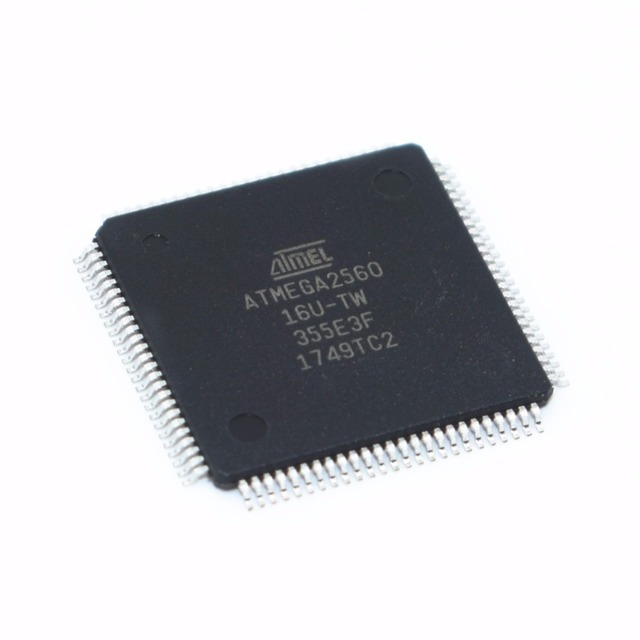
Reverse Engineering Chip ATmega2560P and copy microcontroller atmega2560p source Code from its flash and eeprom memory, rewrite firmware heximal to new processor atmega2560p to make MCU cloning units;
When this bit is written to one, and the I-flag in the Status Register is set (interrupts globally enabled), the Timer/Countern Input Capture interrupt is enabled. The corresponding Interrupt Vector (See “Interrupts” on page 69.) is executed when the ICFn Flag, located in TIFRn, is set.
Bit 3 – OCIEnC: Timer/Countern, Output Compare C Match Interrupt Enable
When this bit is written to one, and the I-flag in the Status Register is set (interrupts globally enabled), the Timer/Countern Output Compare C Match interrupt is enabled. The corresponding Interrupt Vector (See “Interrupts” on page 69.) is executed when the OCFnC Flag, located in TIFRn, is set.
Bit 2 – OCIEnB: Timer/Countern, Output Compare B Match Interrupt Enable
When this bit is written to one, and the I-flag in the Status Register is set (interrupts globally enabled), the Timer/Countern Output Compare B Match interrupt is enabled. The corresponding Interrupt Vector (See “Interrupts” on page 69.) is executed when the OCFnB Flag, located in TIFRn, is set before copy microcontroller pic16c771 firmware.
Bit 1 – OCIEnA: Timer/Countern, Output Compare A Match Interrupt Enable
When this bit is written to one, and the I-flag in the Status Register is set (interrupts globally enabled), the Timer/Countern Output Compare A Match interrupt is enabled. The corresponding Interrupt Vector (See “Interrupts” on page 69.) is executed when the OCFnA Flag, located in TIFRn, is set.
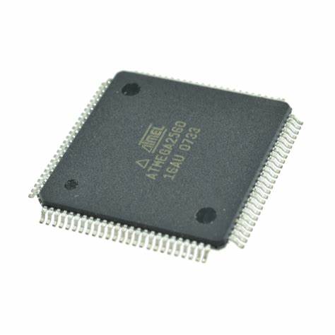
unlock atmega2560p atmel microcomputer protection and copy atmega2560p mcu chip memory content
Bit 0 – TOIEn: Timer/Countern, Overflow Interrupt Enable
When this bit is written to one, and the I-flag in the Status Register is set (interrupts globally enabled), the Timer/Countern Overflow interrupt is enabled. The corresponding Interrupt Vector (See “Interrupts” on page 69.) is executed when the TOVn Flag, located in TIFRn, is set.
Bit 5 – ICFn: Timer/Countern, Input Capture Flag
This flag is set when a capture event occurs on the ICPn pin. When the Input Capture Register (ICRn) is set by the WGMn3:0 to be used as the TOP value, the ICFn Flag is set when the counter reaches the TOP value.
 Posted in
Break IC ATmega1281A Flash
Break IC ATmega1281A and copy microcontroller atmega128a Flash content in the format of heximal, the fuse bit of mcu atmega1281a will be unlocked by focus ion beam technique;
The Timer/Counter is a synchronous design and the timer clock (clkTn) is therefore shown as a clock enable signal in the following figures.
The figures include information on when Interrupt Flags are set, and when the OCRnx Register is updated with the OCRnx buffer value (only for modes utilizing double buffering). Figure 58 shows a timing diagram for the setting of OCFnx.
The COMnA1:0, COMnB1:0, and COMnC1:0 control the output compare pins (OCnA, OCnB, and OCnC respectively) behavior. If one or both of the COMnA1:0 bits are written to one, the OCnA output overrides the normal port functionality of the I/O pin it is connected to when recover chip atmega1281pv flash.
If one or both of the COMnB1:0 bits are written to one, the OCnB output overrides the normal port functionality of the I/O pin it is connected to.
If one or both of the COMnC1:0 bits are written to one, the OCnC output overrides the normal port functionality of the I/O pin it is connected to. However, note that the Data Direction Register (DDR) bit corresponding to the OCnA, OCnB or OCnC pin must be set in order to enable the output driver.
When the OCnA, OCnB or OCnC is connected to the pin, the function of the COMnx1:0 bits is dependent of the WGMn3:0 bits setting. Table 79 shows the COMnx1:0 bit functionality when the WGMn3:0 bits are set to a normal or a CTC mode (non-PWM) if recover mcu atmega169pa code.
Combined with the WGMn3:2 bits found in the TCCRnB Register, these bits control the counting sequence of the counter, the source for maximum (TOP) counter value, and what type of waveform generation to be used, see Table 82.
Modes of operation supported by the Timer/Counter unit are: Normal mode (counter), Clear Timer on Compare match (CTC) mode, and three types of Pulse Width Modulation (PWM) modes. (See “Modes of Operation” on page 147.).
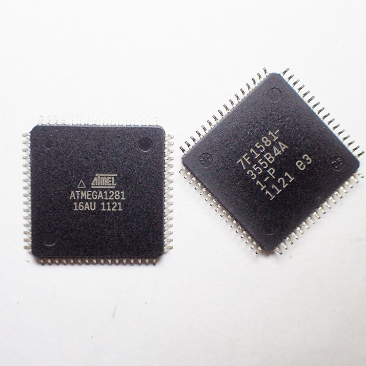
recover atmega1281 microcontroller embedded firmware and crack atmega1281 mcu fuse bit
Setting this bit (to one) activates the Input Capture Noise Canceler. When the Noise Canceler is activated, the input from the Input Capture Pin (ICPn) is filtered. The filter function requires four successive equal valued samples of the ICPn pin for changing its output after recover chip atmega128apv source code.
The input capture is therefore delayed by four Oscillator cycles when the noise canceler is enabled.
This bit selects which edge on the Input Capture Pin (ICPn) that is used to trigger a capture event. When the ICESn bit is written to zero, a falling (negative) edge is used as trigger, and when the ICESn bit is written to one, a rising (positive) edge will trigger the capture.
When a capture is triggered according to the ICESn setting, the counter value is copied into the Input Capture Register (ICRn). The event will also set the Input Capture Flag (ICFn), and this can be used to cause an Input Capture Interrupt, if this interrupt is enabled.
When the ICRn is used as TOP value (see description of the WGMn3:0 bits located in the TCCRnA and the TCCRnB Register), the ICPn is disconnected and consequently the input capture function is disabled.
The FOCnA/FOCnB/FOCnC bits are only active when the WGMn3:0 bits specifies a non-PWM mode. When writing a logical one to the FOCnA/FOCnB/FOCnC bit, an immediate compare match is forced on the waveform generation unit.
Break IC ATmega169PV Program
Break IC ATmega169PV encrypted protection, crack MCU ATmega169PV will help to extract program from microcontroller ATmega169PV and copy the firmware in the format of heximal to new MCU;
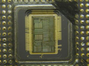
Break IC ATmega169PV encrypted protection, crack MCU ATmega169PV will help to extract program from microcontroller ATmega169PV and copy the firmware in the format of heximal to new MCU
The phase correct Pulse Width Modulation or phase correct PWM mode (WGMn3:0 = 1, 2, 3, 10, or 11) provides a high resolution phase correct PWM waveform generation option. The phase correct PWM mode is, like the phase and frequency correct PWM mode, based on a dual-slope operation. The counter counts repeatedly from BOTTOM (0x0000) to TOP and then from TOP to BOTTOM.
In non-inverting Compare Output mode, the Output Compare (OCnx) is cleared on the compare match between TCNTn and OCRnx while upcounting, and set on the compare match while downcounting. In inverting Output Compare mode, the operation is inverted. The dual-slope operation has lower maximum operation frequency than single slope operation after recover mcu P89LPC925FDH heximal.
However, due to the symmetric feature of the dual-slope PWM modes, these modes are preferred for motor control applications. The PWM resolution for the phase correct PWM mode can be fixed to 8-, 9-, or 10-bit, or defined by either ICRn or OCRnA. The minimum resolution allowed is 2-bit (ICRn or OCRnA set to 0x0003), and the maximum resolution is 16-bit (ICRn or OCRnA set to MAX).
The PWM resolution in bits can be calculated by using the following equation: In phase correct PWM mode the counter is incremented until the counter value matches either one of the fixed values 0x00FF, 0x01FF, or 0x03FF (WGMn3:0 = 1, 2, or 3), the value in ICRn (WGMn3:0 = 10), or the value in OCRnA (WGMn3:0 = 11).
The counter has then reached the TOP and changes the count direction. The TCNTn value will be equal to TOP for one timer clock cycle. The timing diagram for the phase correct PWM mode is shown on Figure 56. The figure shows phase correct PWM mode when OCRnA or ICRn is used to define TOP before Break MCU dsPIC30F4011 hex program.
The TCNTn value is in the timing diagram shown as a histogram for illustrating the dual-slope operation. The diagram includes non-inverted and inverted PWM outputs. The small horizontal line marks on the TCNTn slopes represent compare matches between OCRnx and TCNTn. The OCnx Interrupt Flag will be set when a compare match occurs after Break microcontroller PIC12F629 program.
The Timer/Counter Overflow Flag (TOVn) is set each time the counter reaches BOTTOM. When either OCRnA or ICRn is used for defining the TOP value, the OCnA or ICFn Flag is set accordingly at the same timer clock cycle as the OCRnx Registers are updated with the double buffer value (at TOP). The Interrupt Flags can be used to generate an interrupt each time the counter reaches the TOP or BOTTOM value.
Break IC PIC16C74B Binary
Break IC PIC16C74B by disabling its security fuse bit, this process will refer to MCU cracking and focus ion beam, Binary inside the program memory of Microcontroller can be extracted and rewrite to new Microprocessor PIC16C74B;
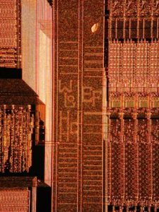
Break IC PIC16C74B by disabling its security fuse bit, this process will refer to MCU cracking and focus ion beam, Binary inside the program memory of Microcontroller can be extracted and rewrite to new Microprocessor PIC16C74B
A variety of frequency ranges and packaging options are available. Depending on application and production requirements, the proper device option can be selected using the information in the PIC16C74B Product Identification System section at the end of this data sheet. When placing orders if copy dsp TMS320LF2401AVFA flash memory, please use that page of the data sheet to specify the correct part number.
For the PIC16C7X family, there are two device “types” as indicated in the device number:
1. C, as in PIC16C74. These devices have EPROM type memory and operate over the standard voltage range.
2. LC, as in PIC16LC74. These devices have EPROM type memory and operate over an extended voltage range after Break IC.
The UV erasable version, offered in windowed CERDIP packages, is optimal for prototype development and pilot programs. This version can be erased and reprogrammed to any of the oscillator modes. Microchip’s PICSTART Plus and PRO MATE II programmers both support programming of the PIC16C63A/65B/73B/74B when Break IC.
The availability of OTP devices is especially useful for customers who need the flexibility for frequent code updates and small volume applications.
The OTP devices, packaged in plastic packages, permit the user to program them once. In addition to the program memory, the configuration bits must also be programmed before chip PIC16F73 program copying.
Microchip offers a QTP Programming Service for factory production orders. This service is made available for users who choose not to program a medium to high quantity of units and whose code patterns have stabilized. The devices are identical to the OTP devices but with all EPROM locations and configuration options already programmed by the factory. Certain code and prototype verification procedures apply before production shipments are available. Please contact your local Microchip Technology sales office for more details.
Microchip offers a unique programming service where a few user-defined locations in each device are programmed with different serial numbers. The serial numbers may be random, pseudo-random or sequential.
Serial programming allows each device to have a unique number, which can serve as an entry code, password or ID number.
The high performance of the PIC16CXX family can be attributed to a number of architectural features commonly found in RISC microprocessors. To begin with, the PIC16CXX uses a Harvard architecture, in which program and data are accessed from separate memories using separate buses.
This improves bandwidth over traditional von Neumann architecture, in which program and data are fetched from the same memory using the same bus. Separating program and data buses further allows instructions to be sized differently than the 8-bit wide data word. Instruction opcodes are 14-bits wide, making it possible to have all single word instructions.
A 14-bit wide program memory access bus fetches a 14-bit instruction in a single cycle. A two-stage pipeline overlaps fetch and execution of instructions (Example 3-1). Consequently, most instructions execute in a single cycle (200 ns @ 20 MHz) except for program branches. All devices covered by this data sheet contain 4K x 14-bit program memory and 192 x 8-bit data memory.
Break Microprocessor ATmega128V Code
Break Microprocessor ATmega128V protected memory and readout code from MCU ATmega128V flash memory, crack MCU ATmega128V protection and disable its security fuse bit;
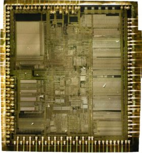
Break Microprocessor ATmega128V protected memory and readout code from MCU ATmega128V flash memory, crack MCU ATmega128V protection and disable its security fuse bit
The fast Pulse Width Modulation or fast PWM mode (WGMn3:0 = 5, 6, 7, 14, or 15) provides a high frequency PWM waveform generation option. The fast PWM differs from the other PWM options by its single-slope operation. The counter counts from BOTTOM to TOP then restarts from BOTTOM.
In non-inverting Compare Output mode, the Output Compare (OCnx) is set on the compare match between TCNTn and OCRnx, and cleared at TOP. In inverting Compare Output mode output is cleared on compare match and set at TOP. Due to the single-slope operation, the operating frequency of the fast PWM mode can be twice as high as the phase correct and phase and frequency correct PWM modes that use dual-slope operation. This high frequency makes the fast PWM mode well suited for power regulation, rectification, and DAC applications.
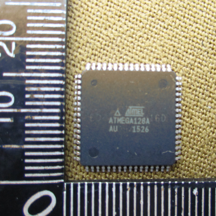
clone atmega128v mcu flash content in heximal or binary of flash memory
High frequency allows physically small sized external components (coils, capacitors), hence reduces total system cost.
The PWM resolution for fast PWM can be fixed to 8-, 9-, or 10-bit, or defined by either ICRn or OCRnA. The minimum resolution allowed is 2-bit (ICRn or OCRnA set to 0x0003), and the maximum resolution is 16-bit (ICRn or OCRnA set to MAX). The PWM resolution in bits can be calculated by using the following equation before microprocessor AT89C4051 hex recovery:
In fast PWM mode the counter is incremented until the counter value matches either one of the fixed values 0x00FF, 0x01FF, or 0x03FF (WGMn3:0 = 5, 6, or 7), the value in ICRn (WGMn3:0 = 14), or the value in OCRnA (WGMn3:0 = 15). The counter is then cleared at the following timer clock cycle. The timing diagram for the fast PWM mode is shown in Figure 55. The figure shows fast PWM mode when OCRnA or ICRn is used to define TOP after break microprocessor code.
The TCNTn value is in the timing diagram shown as a histogram for illustrating the single-slope operation. The diagram includes non-inverted and inverted PWM outputs. The small horizontal line marks on the TCNTn slopes represent compare matches between OCRnx and TCNTn. The OCnx Interrupt Flag will be set when a compare match occurs when recover microprocessor PIC18F2520 bin.
The Timer/Counter Overflow Flag (TOVn) is set each time the counter reaches TOP. In addition the OCnA or ICFn Flag is set at the same timer clock cycle as TOVn is set when either OCRnA or ICRn is used for defining the TOP value. If one of the interrupts are enabled, the interrupt handler routine can be used for updating the TOP and compare values.
When changing the TOP value the program must ensure that the new TOP value is higher or equal to the value of all of the Compare Registers. If the TOP value is lower than any of the Compare Registers, a compare match will never occur between the TCNTn and the OCRnx. Note that when using fixed TOP values the unused bits are masked to zero when any of the OCRnx Registers are written.
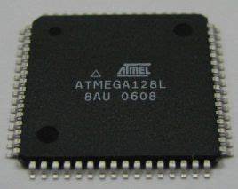
reverse engineering atmega128v mcu fuse bit and readout embedded flash program and eeprom data of hexima or binary
The procedure for updating ICRn differs from updating OCRnA when used for defining the TOP value. The ICRn Register is not double buffered. This means that if ICRn is changed to a low value when the counter is running with none or a low prescaler value, there is a risk that the new ICRn value written is lower than the current value of TCNTn before rec0ver microprocessor MC68HC11A0FN3 bin.
The result will then be that the counter will miss the compare match at the TOP value. The counter will then have to count to the MAX value (0xFFFF) and wrap around starting at 0x0000 before the compare match can occur. The OCRnA Register however, is double buffered. This feature allows the OCRnA I/O location to be written anytime.
When the OCRnA I/O location is written the value written will be put into the OCRnA Buffer Register. The OCRnA Compare Register will then be updated with the value in the Buffer Register at the next timer clock cycle the TCNTn matches TOP. The update is done at the same timer clock cycle as the TCNTn is cleared and the TOVn Flag is set.
Break IC ATmega128V Heximal
Break IC ATmega128V memory and extract heximal from MCU flash and eeprom memory, unlock microcontroller atmega128v protection set up by the designer and manufacturer;
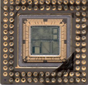
Break IC ATmega128V memory and extract heximal from MCU flash and eeprom memory, unlock microcontroller atmega128v protection set up by the designer and manufacturer
The general I/O port function is overridde by the Output Compare (OCnx) from the Waveform Generator if either of the COMnx1:0 bits are set. However, the OCnx pin direction (input or output) is still controlled by the Data Direction Register (DDR) for the port pin when copy IC atmega8l heximal.
The Data Direction Register bit for the OCnx pin (DDR_OCnx) must be set as output before the OCnx value is visible on the pin. The port override function is generally independent of the Waveform Generation mode, but there are some exceptions if recover IC STM32F107RCT6 code.
The design of the Output Compare pin logic allows initialization of the OCnx state before the output is enabled. Note that some COMnx1:0 bit settings are reserved for certain modes of operation.
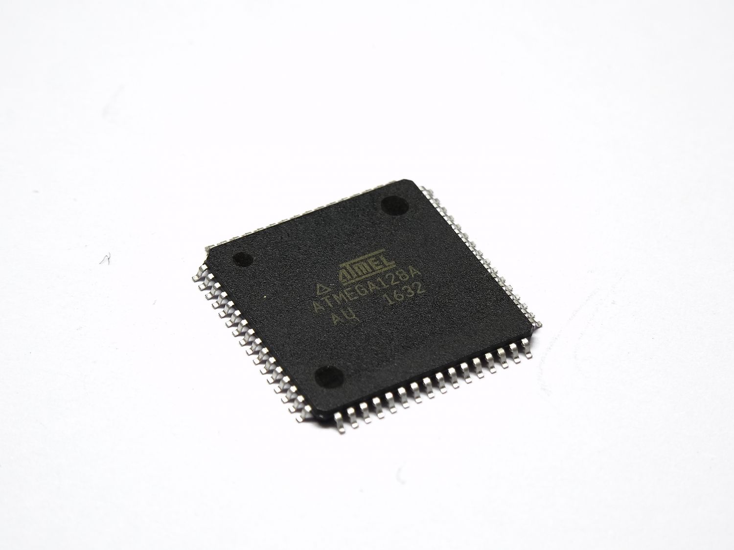
crack secured mcu atmega128v fuse bit and extract firmware program from flash memory
The Waveform Generator uses the COMnx1:0 bits differently in normal, CTC, and PWM modes. For all modes, setting the COMnx1:0 = 0 tells the Waveform Generator that no action on the OCnx Register is to be performed on the next compare match when copy microcontroller pic16f684 firmware.
A change of the COMnx1:0 bits state will have effect at the first compare match after the bits are written. For non-PWM modes, the action can be forced to have immediate effect by using the FOCnx strobe bits.
The mode of operation, i.e., the behavior of the Timer/Counter and the Output Compare pins, is defined by the combination of the Waveform Generation mode (WGMn3:0) and Compare Output mode (COMnx1:0) bits.
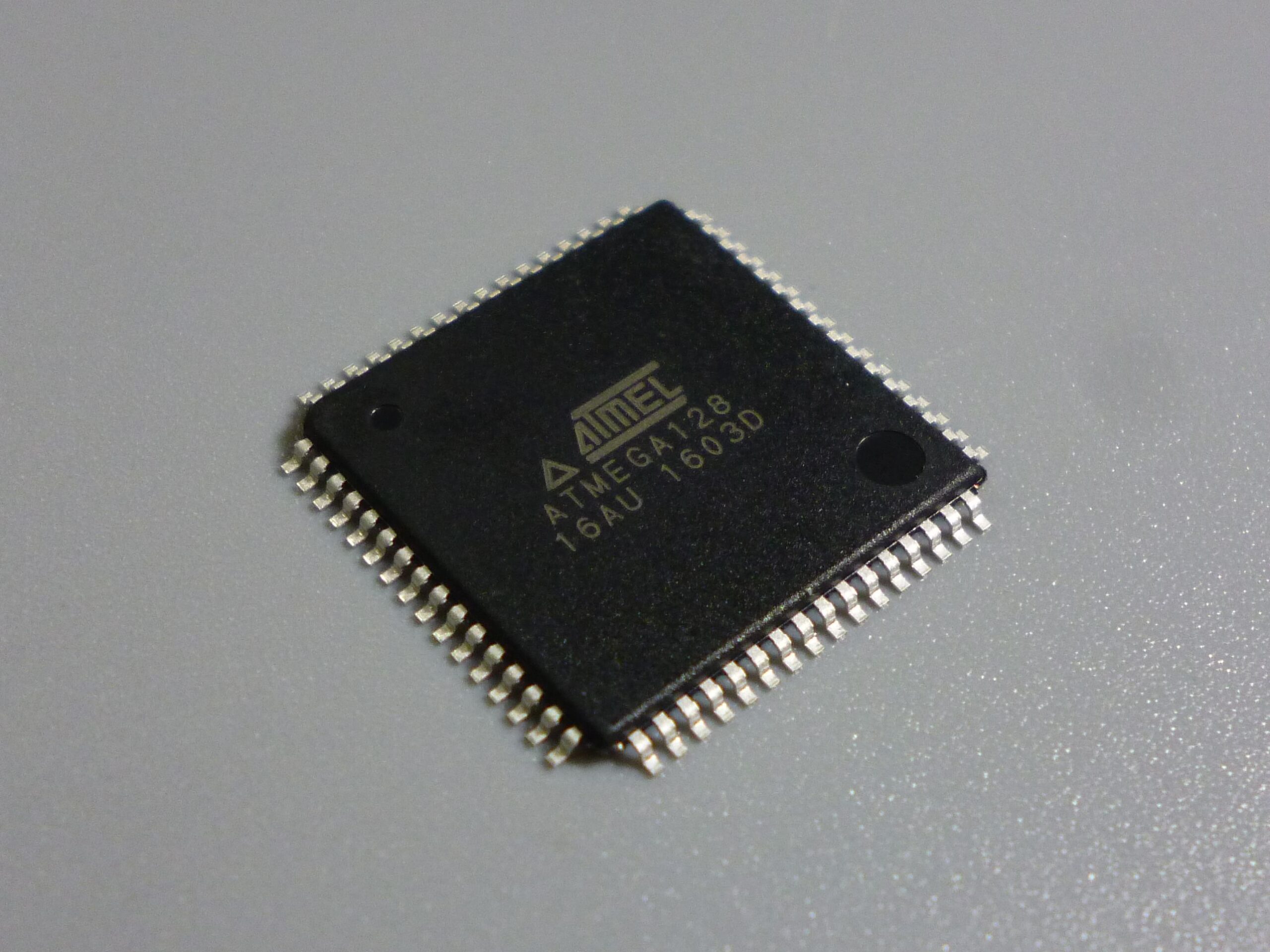
unlock ATMEGA128V microcontroller flash memory program
The Compare Output mode bits do not affect the counting sequence, while the Waveform Generation mode bits do. The COMnx1:0 bits control whether the PWM output generated should be inverted or not (inverted or non-inverted PWM). For non-PWM modes the COMnx1:0 bits control whether the output should be set, cleared or toggle at a compare match.
Break IC ATMEGA1280A Binary
Break IC ATmega1280A microcontroller tamper resistance system and recover atmega1280a microprocessor fuse bit, readout embedded firmware file from flash memory and eeprom memory;
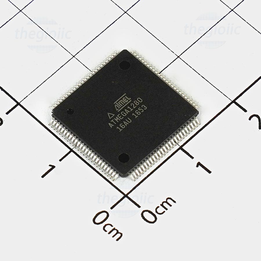
Break IC ATmega1280A microcontroller tamper resistance system and decrypt atmega1280a microprocessor fuse bit, readout embedded firmware file from flash memory and eeprom memory
The 16-bit Timer/Counter unit allows accurate program execution timing (event management), wave generation, and signal timing measurement. The main features are:
True 16-bit Design (i.e., Allows 16-bit PWM)
Three independent Output Compare Units
Double Buffered Output Compare Registers
One Input Capture Unit
Input Capture Noise Canceler
Clear Timer on Compare Match (Auto Reload)
Glitch-free, Phase Correct Pulse Width Modulator (PWM)
Variable PWM Period
Frequency Generator
External Event Counter
Twenty independent interrupt sources (TOV1, OCF1A, OCF1B, OCF1C, ICF1, TOV3,
OCF3A, OCF3B, OCF3C, ICF3, TOV4, OCF4A, OCF4B, OCF4C, ICF4, TOV5, OCF5A, OCF5B, OCF5C and ICF5)
Most register and bit references in this section are written in general form. A lower case “n” replaces the Timer/Counter number, and a lower case “x” replaces the Output Compare unit channel. However, when using the register or bit defines in a program, the precise form must be used, i.e., TCNT1 for accessing Timer/Counter1 counter value and so on.
A simplified block diagram of the 16-bit Timer/Counter is shown in Figure 49. For the actual placement of I/O pins, see “Pinout ATmega640/1280/2560” on page 2 and “Pinout ATmega1281/2561” on page 3. CPU accessible I/O Registers, including I/O bits and I/O pins, are shown in bold when crack mcu atmega1280 eeprom and flash memory.
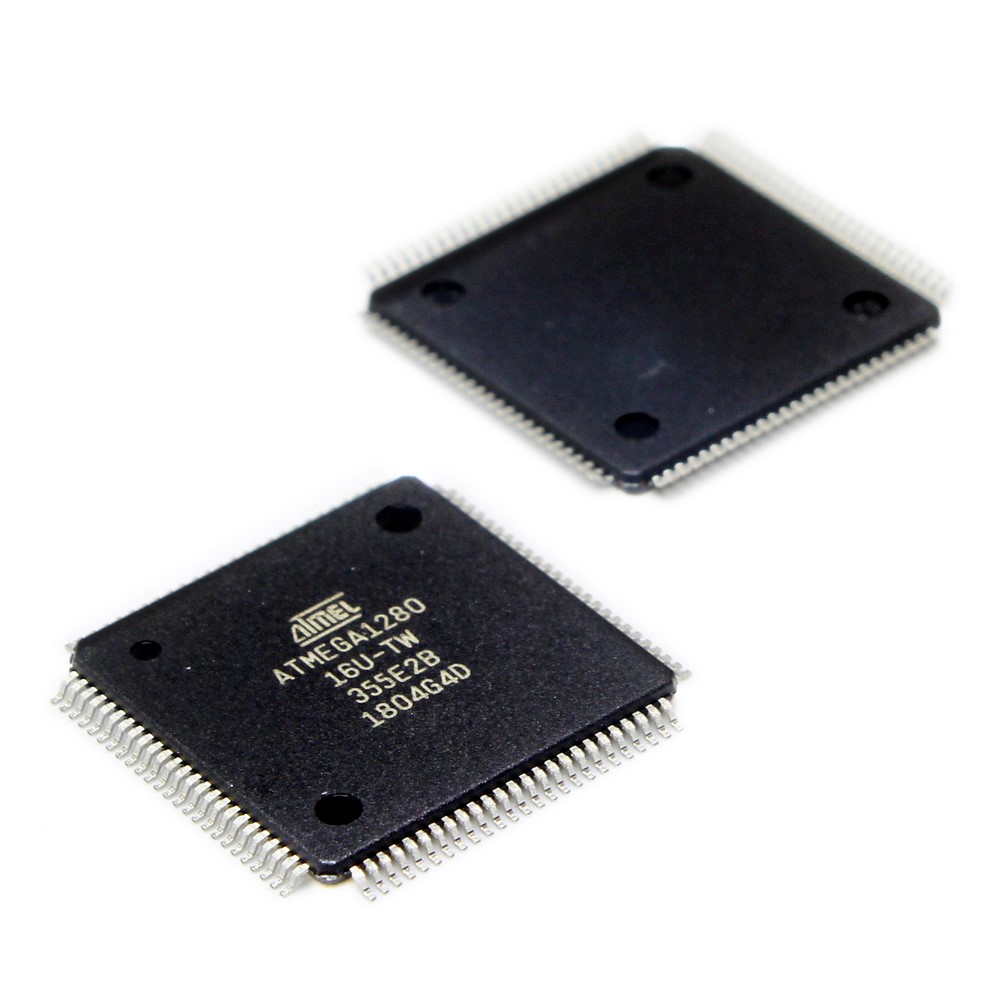
hack locked atmega1280a mcu flash memory after decap microcontroller atmega1280a mcu package and dump heximal code from flash memory
The device-specific I/O Register and bit locations are listed in the “16-bit Timer/Counter Register Description”.
The Power Reduction Timer/Counter1 bit, PRTIM1, in “Power Reduction Register 0 – PRR0” on page 54 must be written to zero to enable Timer/Counter1 module.
The Power Reduction Timer/Counter3 bit, PRTIM3, in “Power Reduction Register 1 – PRR1” on page 55 must be written to zero to enable Timer/Counter3 module.
The Power Reduction Timer/Counter4 bit, PRTIM4, in “Power Reduction Register 1 – PRR1” on page 55 must be written to zero to enable Timer/Counter4 module.
The Power Reduction Timer/Counter5 bit, PRTIM5, in “Power Reduction Register 1 – PRR1” on page 55 must be written to zero to enable Timer/Counter5 module.
Timer/Counter4 and Timer/Counter5 only have full functionality in the ATmega640/1280/2560.
The Timer/Counter (TCNTn), Output Compare Registers (OCRnA/B/C), and Input Capture Register (ICRn) are all 16-bit registers.
Special procedures must be followed when accessing the 16-bit registers. These procedures are described in the section “Accessing 16-bit Registers” on page 137. The Timer/Counter Control Registers (TCCRnA/B/C) are 8-bit registers and have no CPU access restrictions.
Interrupt requests (shorten as Int.Req.) signals are all visible in the Timer Interrupt Flag Register (TIFRn). All interrupts are individually masked with the Timer Interrupt Mask Register (TIMSKn). TIFRn and TIMSKn are not shown in the figure since these registers are shared by other timer units.
The Timer/Counter can be clocked internally, via the prescaler, or by an external clock source on the Tn pin. The Clock Select logic block controls which clock source to readout locked mcu atmega1280v flash program and edge the Timer/Counter uses to increment (or decrement) its value. The Timer/Counter is inactive when no clock source is selected. The output from the clock select logic is referred to as the timer clock (clkTn).
The double buffered Output Compare Registers (OCRnA/B/C) are compared with the Timer/Counter value at all time. The result of the compare can be used by the Waveform Generator to generate a PWM or variable frequency output on the Output Compare pin (OCnA/B/C). See “Output Compare Units” on page 144.. The compare match event will also set the Compare Match Flag (OCFnA/B/C) which can be used to generate an Output Compare interrupt request.
Break MCU ATmega1280PV Code
Break MCU ATmega1280PV Code can help engineer to recover embedded firmware such as heximal from flash memory and atmega128 microcontroller;
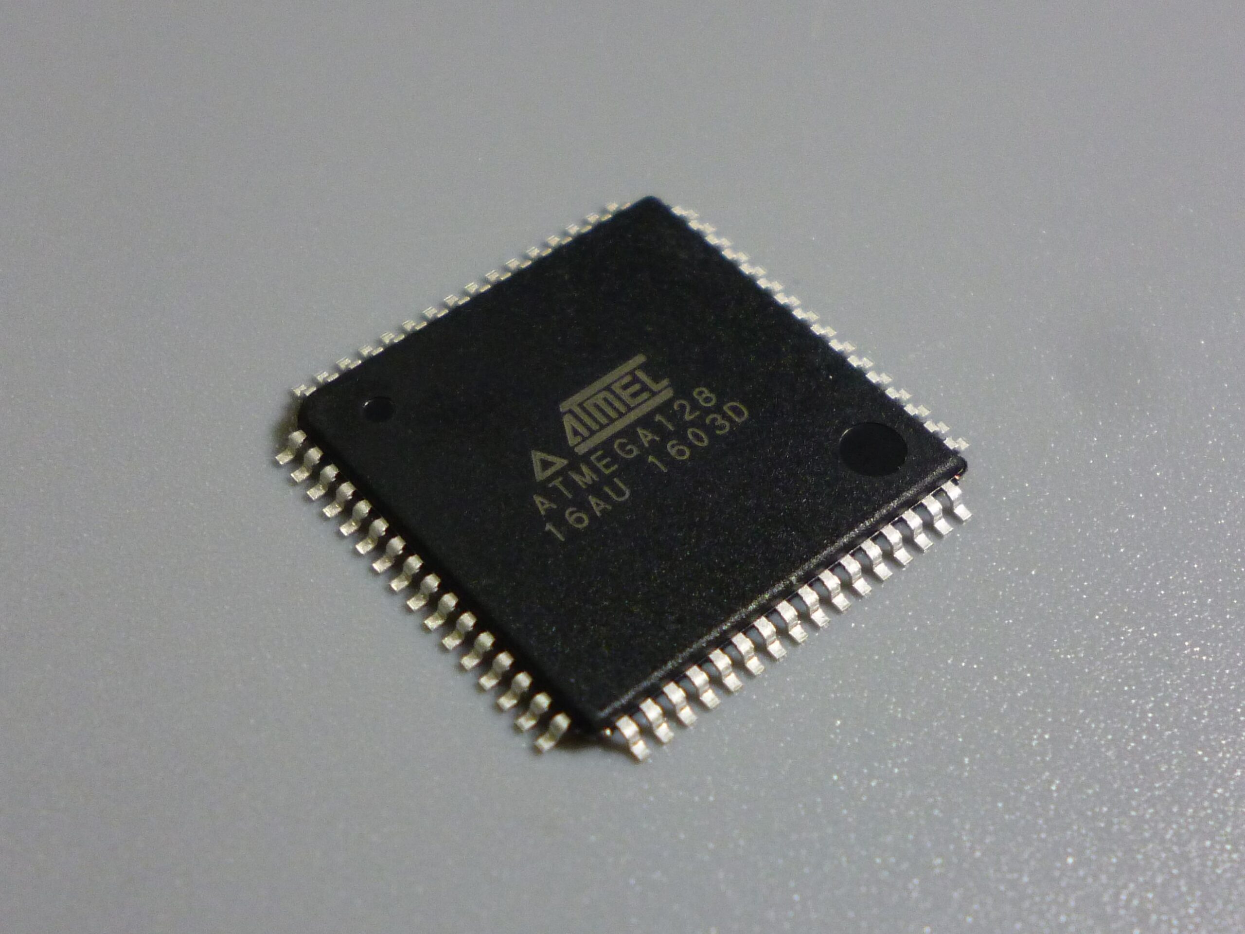
Break MCU ATmega1280PV Code can help engineer to recover embedded firmware such as heximal from flash memory and atmega128 microcontroller;
The FOC0A bit is only active when the WGM bits specify a non-PWM mode. However, for ensuring compatibility with future devices, this bit must be set to zero when TCCR0B is written when operating in PWM mode.
When writing a logical one to the FOC0A bit, an immediate Compare Match is forced on the Waveform Generation unit.
The OC0A output is changed according to its COM0A1:0 bits setting. Note that the FOC0A bit is implemented as a strobe. Therefore it is the value present in the COM0A1:0 bits that determines the effect of the forced compare. A FOC0A strobe will not generate any interrupt, nor will it clear the timer in CTC mode using OCR0A as TOP in the process of breaking off atmega128 microcontroller protection. The FOC0A bit is always read as zero. The FOC0B bit is only active when the WGM bits specify a non-PWM mode.
However, for ensuring compatibility with future devices, this bit must be set to zero when TCCR0B is written when operating in PWM mode. When writing a logical one to the FOC0B bit, an immediate Compare Match is forced on the Waveform Generation unit.The OC0B output is changed according to its COM0B1:0 bits setting. Note that the FOC0B bit is implemented as a strobe.
Therefore it is the value present in the COM0B1:0 bits that determines the effect of the forced compare. A FOC0B strobe will not generate any interrupt, nor will it clear the timer in CTC mode using OCR0B as TOP. The FOC0B bit is always read as zero. The Timer/Counter Register gives direct access, both for read and write operations, to the Timer/Counter unit 8-bit counter. Writing to the TCNT0 Register blocks (removes) the Compare Match on the following timer clock.
Modifying the counter (TCNT0) while the counter is running, introduces a risk of missing a Compare Match between TCNT0 and the OCR0x Registers. The Output Compare Register A contains an 8-bit value that is continuously compared with the counter value (TCNT0). A match can be used to generate an Output Compare interrupt, or to generate a waveform output on the OC0A pin.
Break Microcontroller ATmega640PV Binary
Break Microcontroller ATmega640PV program memory, and readout binary from MCU ATmega640PV, the firmware will include content from both eeprom and flash memory;
Break Microcontroller ATmega640PV program memory, and readout binary from MCU ATmega640PV, the firmware will include content from both eeprom and flash memory
In Clear Timer on Compare or CTC mode (WGM02:0 = 2), the OCR0A Register is used to manipulate the counter resolution.
In CTC mode the counter is cleared to zero when the counter value (TCNT0) matches the OCR0A. The OCR0A defines the top value for the counter, hence also its resolution.
This mode allows greater control of the Compare Match output frequency. It also simplifies the operation of counting external events.
The timing diagram for the CTC mode is shown in Figure 42. The counter value (TCNT0) increases until a Compare Match occurs between TCNT0 and OCR0A, and then counter (TCNT0) is cleared if reverse engineering microcontroller PIC16C620 code.
An interrupt can be generated each time the counter value reaches the TOP value by using the OCF0A Flag.
If the interrupt is enabled, the interrupt handler routine can be used for updating the TOP value. However, changing TOP to a value close to BOTTOM when the counter is running with none or a low prescaler value must be done with care since the CTC mode does not have the double buffering feature.
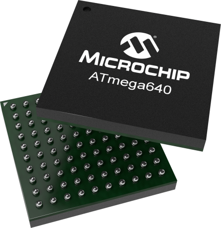
unlock avr mcu atmega640pv protection and copy embedded firmware from flash and eeprom memory
If the new value written to OCR0A is lower than the current value of TCNT0, the counter will miss the Compare Match.
The counter will then have to count to its maximum value (0xFF) and wrap around starting at 0x00 before the Compare Match can occur after microcontroller PIC16F620A binary recovery.
For generating a waveform output in CTC mode, the OC0A output can be set to toggle its logical level on each Compare Match by setting the Compare Output mode bits to toggle mode (COM0A1:0 = 1). The OC0A value will not be visible on the port pin unless the data direction for the pin is set to output.
The waveform generated will have a maximum frequency of fOC0 = fclk_I/O/2 when OCR0A is set to zero (0x00). The waveform frequency is defined by the following equation;
Break Microcontroller PIC24FJ16GA002 Heximal
Break Microcontroller PIC24FJ16GA002 program memory and data memory, readout heximal from MCU PIC24FJ16GA002 for microprocessor cloning.
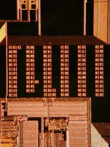
Break Microcontroller PIC24FJ16GA002 program memory and data memory, readout heximal from MCU PIC24FJ16GA002 for microprocessor cloning
The mode of operation, i.e., the behavior of the Timer/Counter and the Output Compare pins, is defined by the combination of the Waveform Generation mode (WGM02:0) and Compare Output mode (COM0x1:0) bits.
The Compare Output mode bits do not affect the counting sequence, while the Waveform Generation mode bits do. The COM0x1:0 bits control whether the PWM output generated should be inverted or not (inverted or non-inverted PWM) if break microcontroller ATmega1284 memory.
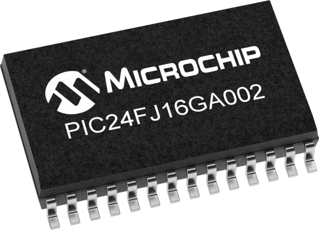
unlock PIC24FJ16GA002 microcontroller fuse bit and clone heximal program from flash memory
For non-PWM modes the COM0x1:0 bits control whether the output should be set, cleared, or toggled at a Compare Match (See “Compare Match Output Unit” on page 146.).For detailed timing information see “Timer/Counter Timing Diagrams”.
The simplest mode of operation is the Normal mode (WGM02:0 = 0). In this mode the counting direction is always up (incrementing), and no counter clear is performed. The counter simply overruns when it passes its maximum 8-bit value (TOP = 0xFF) and then restarts from the bottom (0x00) when microcontroller ATmega1284V memory reverse engineering.
In normal operation the Timer/Counter Overflow Flag (TOV0) will be set in the same timer clock cycle as the TCNT0 becomes zero. The TOV0 Flag in this case behaves like a ninth bit, except that it is only set, not cleared.
attack PIC24FJ16GA002 mcu protection and restore flash memory program and data file
However, combined with the timer overflow interrupt that automatically clears the TOV0 Flag, the timer resolution can be increased by software. There are no special cases to consider in the Normal mode, a new counter value can be written anytime. The Output Compare Unit can be used to generate interrupts at some given time.
Using the Output Compare to generate waveforms in Normal mode is not recommended, since this will occupy too much of the CPU time.