Archive for the ‘Break IC’ Category
 Break MCU AT89C5131A Binary
 May 29th, 2010 |
  Author:
 The ATMEL AT89C5131A is a powerful microcontroller (MCU) widely adopted across industries due to its versatility and integrated USB interface. As part of the AT89C51 family, it combines a high-performance 8-bit microprocessor core with on-chip flash, EEPROM, and multiple communication peripherals. These features make it highly reliable for use in industrial controllers, consumer devices, medical equipment, and security products. However, when the firmware becomes inaccessible, or the binary program is locked by security settings, companies may require specialized services to break MCU AT89C5131A binary for legitimate recovery, duplication, or system maintenance.
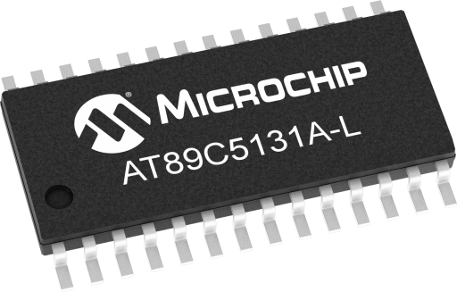
The AT89C5131A is commonly applied in:
- Industrial Control Systems – handling automation tasks, sensor data management, and device control.
- Medical Electronics – used in diagnostic instruments where stable firmware and reliable memory archives are essential.
- Consumer Electronics – powering USB-based devices, smart accessories, and portable tools.
- Security Systems – embedded in access control solutions and cryptographic devices, where secured and encrypted programs protect sensitive data.
These real-world applications highlight the importance of the source code and binary files stored in the chip’s flash and EEPROM memory. When a system malfunctions or legacy firmware is required, the ability to retrieve, restore, or replicate these files becomes critical.
Break MCU AT89C5131A needs to unlock microcontroller at89c5131a fuse bit among flash memory and processor, then extract ic chip Binary from it;
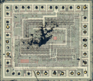
AT89C5130A/31A-M is a high-performance Flash version of the 80C51 single-chip 8-bit micro-controllers with full speed USB functions. AT89C5130A/31A-M features a full-speed USB module compatible with the USB specifications Version 1.1 and 2.0.
The AT89C5131A includes strong protection mechanisms to secure its embedded program from unauthorized readout or copying. Once code protection is enabled, the device’s flash memory becomes locked, preventing standard access. Key difficulties include:
- Secured Flash and EEPROM – Direct extraction of firmware is blocked by built-in protection bits.
- Encrypted Program Storage – Data is often stored in protected formats, requiring advanced decode and decrypt expertise.
- Tamper Resistance – Some chips may erase their memory if invasive attack attempts are detected.
- Reverse Engineering Complexity – Even if partial dump files are collected, reconstructing complete heximal archives demands expert knowledge.
These challenges mean that attempts to unlock, hack, or decapsulate the device require highly specialized approaches.
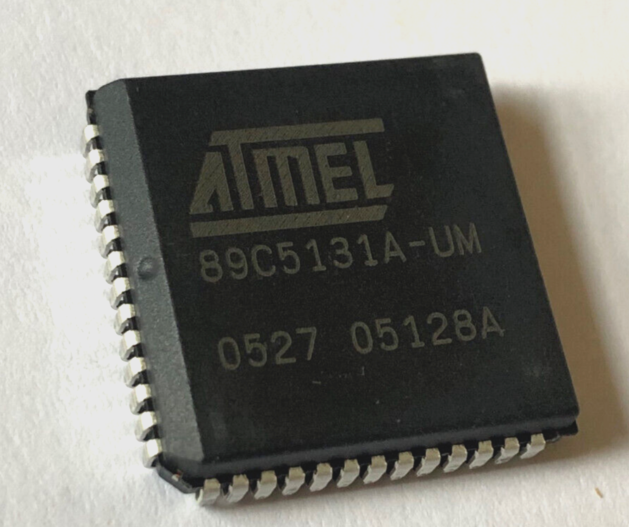
This module integrates the USB transceivers with a 3.3V voltage regulator and the Serial Interface Engine (SIE) with Digital Phase Locked Loop and 48 MHz clock recovery after recover stm32f107rct6 MCU.
USB Event detection logic (Reset and Suspend/Resume) and FIFO buffers supporting the mandatory control Endpoint (EP0) and up to 6 versatile Endpoints (EP1/EP2/EP3/EP4/EP5/EP6) with minimum software overhead are also part of the USB module.
AT89C5130A/31A-M retains the features of the Atmel 80C52 with extended Flash capacity (16/32-Kbytes), 256 bytes of internal RAM, a 4-level interrupt system, two 16-bit timer/counters (T0/T1), a full duplex enhanced UART (EUART) and an on-chip oscillator.
In addition, AT89C5130A/31A-M has an on-chip expanded RAM of 1024 bytes (ERAM), a dual data pointer, a 16-bit up/down Timer (T2), a Programmable Counter Array (PCA), up to 4 programmable LED current sources, a programmable hardware watchdog and a power-on reset for copy at89s8252 MCU flash.
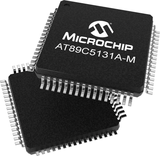
We provide the complete solution for organizations needing to break MCU AT89C5131A binary in a secure, reliable, and legally compliant manner. Our team combines advanced reverse engineering expertise with precision tools to extract, readout, and recover embedded firmware while maintaining the integrity of the original chip.
Our services include:
- Firmware Recovery and Restoration – enabling customers to restore essential files from locked devices.
- Cloning and Replication – safely duplicate or copy the program onto new hardware for production continuity.
- Legacy System Support – helping industries extend the life of older systems by retrieving embedded firmware.
We do not simply attempt brute-force attacks; instead, we employ professional methods that minimize risk, preserve data, and ensure consistent results.
AT89C5130A/31A-M has two software-selectable modes of reduced activity for further reduction in power consumption. In the idle mode the CPU is frozen while the timers, the serial ports and the interrupt system are still operating. In the power-down mode the RAM is saved, the peripheral clock is frozen, but the device has full wake-up capability through USB events or external interrupts.
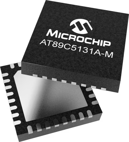
The need to break MCU AT89C5131A binary arises when businesses face locked or inaccessible systems that hinder ongoing operations. With applications across critical industries, the ability to recover, replicate, and restore firmware is invaluable. Our proven services offer a perfect solution, ensuring that your secured MCU can be successfully unlocked and its binary data fully retrieved for future use.
 Posted in Break IC |
  Tags: break mcu locked archive, break mcu locked code, break mcu locked dump, break mcu locked eeprom, break mcu locked firmware, break mcu locked information, break mcu locked memory, break mcu locked program, знаходзіць зноў locked mcu binary, знаходзіць зноў locked mcu data, знаходзіць зноў locked mcu eeprom, знаходзіць зноў locked mcu file, знаходзіць зноў locked mcu firmware, знаходзіць зноў locked mcu heximal, знаходзіць зноў locked mcu memory, знаходзіць зноў locked mcu program |
  Comments Closed
Break Chip PIC12C509 Code
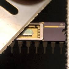
Break Chip PIC12C509 and extract mcu pic12c509 Code from embedded flash memory, microcontroller pic12c509 memory program will be readout after crack fuse bit by focus ion beam technique;
For an CHIP to act as a master CHIP, it can use a 9-bit character frame format (UCSZn = 7). The ninth bit (TXB8n) must be set when an address frame (TXB8n = 1) or cleared when a data frame (TXB = 0) is being transmitted.
The slave CHIPs must in this case be set to use a 9-bit character frame format. The following procedure should be used to exchange data in Multi-processor Communication mode:
All Slave CHIPs are in Multi-processor Communication mode (MPCMn in UCS-RnA is set).
The Master CHIP sends an address frame, and all slaves receive and break this frame. In the Slave CHIPs, the RXCn Flag in UCSRnA will be set as normal before reverse atmega162 CHIP heximal code.
Each Slave CHIP breaks the UDRn Register and determines if it has been selected. If so, it clears the MPCMn bit in UCSRnA, otherwise it waits for the next address byte and keeps the MPCMn setting.
The addressed CHIP will receive all data frames until a new address frame is received. The other Slave CHIPs, which still have the MPCMn bit set, will ignore the data frames.
When the last data frame is received by the addressed CHIP, the addressed CHIP sets the MPCMn bit and waits for a new address frame from master. The process then repeats from 2 if recover pic16f54c CHIP program.
Using any of the 5- to 8-bit character frame formats is possible, but impractical since the Receiver must change between using n and n+1 character frame formats.
This makes full-duplex operation difficult since the Transmitter and Receiver uses the same character size setting. If 5- to 8-bit character frames are used, the Transmitter must be set to use two stop bit (USBSn = 1) since the first stop bit is used for indicating the frame type.
Do not use Break-Modify-Write instructions (SBI and CBI) to set or clear the MPCMn bit. The MPCMn bit shares the same I/O location as the TXCn Flag and this might accidentally be cleared when using SBI or CBI instructions.
Break IC PIC16C57C Firmware
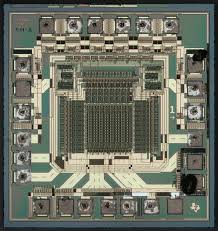
Break IC PIC16C57C Firmware is a process to unlock microcontroller pic16c57c encryptive system and then extract the embedded flash program from mcu pic16c57c memory;
The Parity Checker is active when the high USART Parity mode (UPMn1) bit is set. Type of Parity Check to be performed (odd or even) is selected by the UPMn0 bit.
When enabled, the Parity Checker calculates the parity of the data bits in incoming frames and compares the result with the parity bit from the serial frame.
The result of the check is stored in the receive buffer together with the received data and stop bits. The Parity Error (UPEn) Flag can then be read by software to check if the frame had a Parity Error before Break IC atmel atmega48pv memory.
The UPEn bit is set if the next character that can be read from the receive buffer had a Parity Error when received and the Parity Checking was enabled at that point (UPMn1 = 1). This bit is valid until the receive buffer (UDRn) is read.
In contrast to the Transmitter, disabling of the Receiver will be immediate. Data from ongoing receptions will therefore be lost. When disabled (i.e., the RXENn is set to zero) the Receiver will no longer override the normal function of the RxDn port pin before read mcu pic16f688 software.
The Receiver buffer FIFO will be flushed when the Receiver is disabled. Remaining data in the buffer will be lost. The receiver buffer FIFO will be flushed when the Receiver is disabled, i.e., the buffer will be emptied of its contents. Unread data will be lost. If the buffer has to be flushed during normal operation, due to for instance an error condition, read the UDRn I/O location until the RXCn Flag is cleared. The following firmware example shows how to flush the receive buffer.
The USART includes a clock recovery and a data recovery unit for handling asynchronous data reception. The clock recovery logic is used for synchronizing the internally generated baud rate clock to the incoming asynchronous serial frames at the RxDn pin after recover mcu st62t65c6 code.
The data recovery logic samples and low pass filters each incoming bit, thereby improving the noise immunity of the Receiver. The asynchronous reception operational range depends on the accuracy of the internal baud rate clock, the rate of the incoming frames, and the frame size in number of bits.
Break Chip ATmega162L Firmware
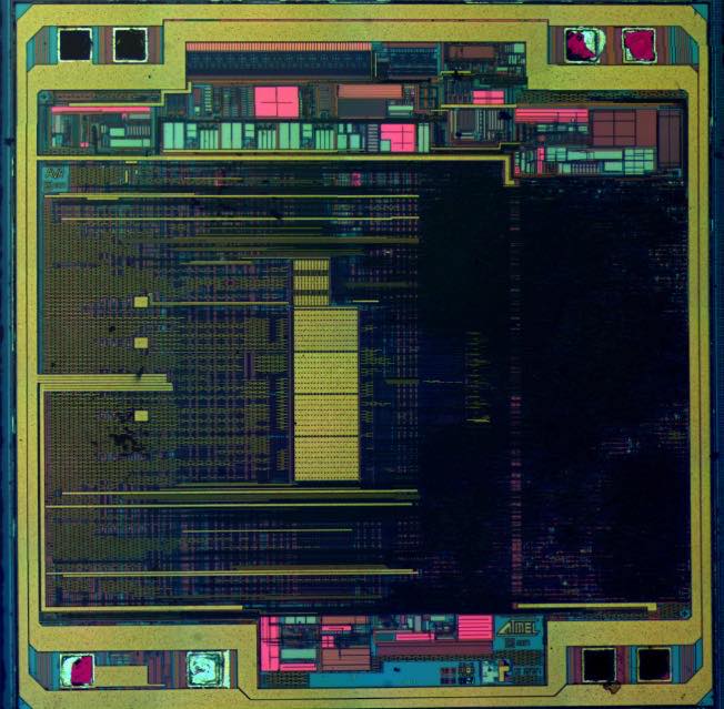
Break Chip ATmega162L and extract mcu atmega162 memory firmware, copy avr atmega162 flash memory content to new mcu atmega162;
If 9-bit characters are used (UCSZn=7) the ninth bit must be break from the RXB8n bit in UCSRnB before breaking the low bits from the UDRn. This rule applies to the FEn, DORn and UPEn Status Flags as well.
Break status from UCSRnA, then data from UDRn. Breaking the UDRn I/O location will change the state of the receive buffer FIFO and consequently the TXB8n, FEn, DORn and UPEn bits, which all are stored in the FIFO, will change if recover microprocessor atmega1281pa flash memory.
The following Firmware example shows a simple USART receive function that handles both nine bit characters and the status bits.
The receive function example breaks all the I/O Registers into the Register File before any computation is done. This gives an optimal receive buffer utilization since the buffer location break will be free to accept new data as early as possible after Break MCU ATmega2560pa hex.
The USART Receiver has one flag that indicates the Receiver state. The Receive Complete (RXCn) Flag indicates if there are unbreak data present in the receive buffer.
This flag is one when unbreak data exist in the receive buffer, and zero when the receive buffer is empty (i.e., does not contain any unbreak data). If the Receiver is disabled (RXENn = 0), the receive buffer will be flushed and consequently the RXCn bit will become zero.
When the Receive Complete Interrupt Enable (RXCIEn) in UCSRnB is set, the USART Receive Complete interrupt will be executed as long as the RXCn Flag is set (provided that global interrupts are enabled).
When interrupt-driven data reception is used, the receive complete routine must break the received data from UDRn in order to clear the RXCn Flag, otherwise a new interrupt will occur once the interrupt routine terminates.
Break MCU PIC18F442 Software
Break MCU PIC18F442 and extract embedded code from microcontroller pic18f442, the encrypted flash memory heximal of microprocessor pic18f442 will be unlocked;

The top of the stack is breakable and writable. Three register locations, TOSU, TOSH and TOSL hold the contents of the stack location pointed to by the STKPTR register. This allows users to implement a software stack if necessary.
After a CALL, RCALL or interrupt, the software can break the pushed value by breaking the TOSU, TOSH and TOSL registers. These values can be placed on a user defined software stack when Break pic16f88 Mcu data.
At return time, the software can replace the TOSU, TOSH and TOSL and do a return. The user must disable the global interrupt enable bits during this time to prevent inadvertent stack operations.
The STKPTR register contains the stack pointer value, the STKFUL (stack full) status bit, and the STKUNF (stack underflow) status bits. Register 4-1 shows the STKPTR register. The value of the stack pointer can be 0 through 31. The stack pointer increments when values are pushed onto the stack and decrements when values are popped off the stack. At RESET, the stack pointer value will be used to Breaking pic12ce518 Mcu.
The user may break and write the stack pointer value. This feature can be used by a Real Time Operating System for return stack maintenance. After the PC is pushed onto the stack 31 times (without popping any values off the stack), the STKFUL bit is set. The STKFUL bit can only be cleared in software or by a POR.
The action that takes place when the stack becomes full depends on the state of the STVREN (Stack Over-flow Reset Enable) configuration bit. Refer to Section 20.0 for a description of the device configuration bits.
If STVREN is set (default), the 31st push will push the (PC + 2) value onto the stack, set the STKFUL bit, and reset the device. The STKFUL bit will remain set and the stack pointer will be set to ‘0’.
If STVREN is cleared, the STKFUL bit will be set on the 31st push and the stack pointer will increment to 31. Any additional pushes will not overwrite the 31st push, and STKPTR will remain at 31.
Since the Top-of-Stack (TOS) is breakable and writable, the ability to push values onto the stack and pull values off the stack without disturbing normal program execution is a desirable option. To push the current PC value onto the stack, a PUSH instruction can be executed.
This will increment the stack pointer and load the current PC value onto the stack. TOSU, TOSH and TOSL can then be modified to place a return address on the stack.
The ability to pull the TOS value off of the stack and replace it with the value that was previously pushed onto the stack, without disturbing normal execution, is achieved by using the POP instruction. ThePOP instruction discards the current TOS by decrementing the stack pointer.
The previous value pushed onto the stack then becomes the TOS value. These resets are enabled by programming the STVREN configuration bit. When the STVREN bit is disabled, a full or underflow condition will set the appropriate STKFUL or STKUNF bit, but not cause a device RESET.
When the STVREN bit is enabled, a full or underflow will set the appropriate STKFUL or STKUNF bit and then cause a device RESET. The STKFUL or STKUNF bits are only cleared by the user software or a POR Reset.
Posted in Break IC |
Tags: break mcu protected archive, break mcu protected binary, break mcu protected code, break mcu protected content, break mcu protected data, break mcu protected eeprom, break mcu protected file, break mcu protected firmware, break mcu protected heximal, break mcu protected information, break mcu protected memory, break mcu protected program |
Comments Closed
Break MCU ATmega162A Heximal
Break MCU ATmega162A and read microcontroller atmega162a memory content out from its secured flash memory, copy Heximal to new atmega162a processor as cloning;
The UCPOLn bit UCRSC selects which XCKn clock edge is used for data sampling and which is used for data change. As Figure 85 shows, when UCPOLn is zero the data will be changed at rising XCKn edge and sampled at falling XCKn edge.
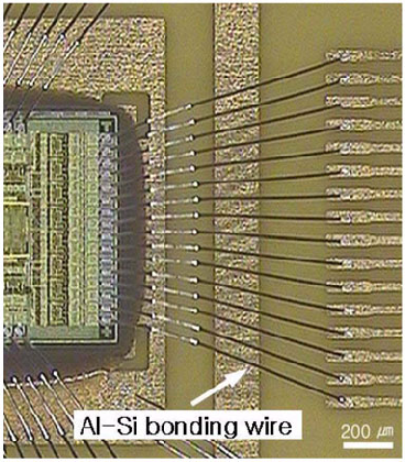
If UCPOLn is set, the data will be changed at falling XCKn edge and sampled at rising XCKn edge. A serial frame is defined to be one character of data bits with synchronization bits (start and stop bits), and optionally a parity bit for error checking. The USART accepts all 30 combinations of the following as valid frame formats if recover microprocessor atmega1281pa flash memory:
1 start bit
5, 6, 7, 8, or 9 data bits
no, even or odd parity bit
1 or 2 stop bits
A frame starts with the start bit followed by the least significant data bit. Then the next data bits, up to a total of nine, are succeeding, ending with the most significant bit. If enabled, the parity bit is inserted after the data bits, before the stop bits.
When a complete frame is transmitted, it can be directly followed by a new frame, or the communication line can be set to an idle (high) state. Figure 86 illustrates the possible combinations of the frame formats. Bits inside brackets are optional.
The frame format used by the USART is set by the UCSZn2:0, UPMn1:0 and USBSn bits in UCSRnB and UCSRnC. The Receiver and Transmitter use the same setting when Break MCU ATmega2560pa heximal.
Note that changing the setting of any of these bits will corrupt all ongoing communication for both the Receiver and Transmitter.
The USART Character SiZe (UCSZn2:0) bits select the number of data bits in the frame. The USART Parity mode (UPMn1:0) bits enable and set the type of parity bit. The selection between one or two stop bits is done by the USART Stop Bit Select (USBSn) bit.
The Receiver ignores the second stop bit. An FE (Frame Error) will therefore only be detected in the cases where the first stop bit is zero. The parity bit is calculated by doing an exclusive-or of all the data bits. If odd parity is used, the result of the exclusive or is inverted. The relation between the parity bit and data bits.
If used, the parity bit is located between the last data bit and first stop bit of a serial frame.
Posted in Break IC |
Tags: break mcu archive, break mcu bin, break mcu code, break mcu content, break mcu data, break mcu eeprom, break mcu file, break mcu firmware, break mcu hex, break mcu information, break mcu memory, break mcu program |
Comments Closed
Break IC PIC12HV615 Heximal
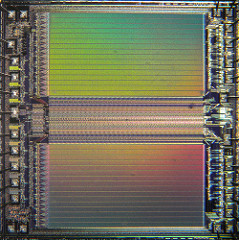
Break IC PIC12HV615 Heximal
We can Break IC PIC12HV615 Heximal, please view the IC PIC12HV615 features for your reference:
To read a program memory location, the user must write two bytes of the address to the PMADRL and PMADRH registers, and then set control bit RD (PMCON1<0>). Once the read control bit is set, the program memory Flash controller will use the second instruction cycle after to read the data.
This causes the second instruction immediately following the “BSF PMCON1,RD” instruction to be ignored. The data is available in the very next cycle in the PMDATL and PMDATH registers; it can be read as two bytes in the following instructions.
PMDATL and PMDATH registers will hold this value until another read or until it is written to by the user (during a write operation). A word of the Flash program memory may only be written to if the word is in an unprotected segment of memory after Break IC.
Flash program memory must be written in four-word blocks. See Figure 3-2 and Figure 3-3 for more details. A block consists of four words with sequential addresses, with a lower boundary defined by an address, where PMADRL<1:0> = 00. All block writes to program memory are done as 16-word erase by four-word write operations. The write operation is edge aligned and cannot occur across boundaries. To write program data, it must first be loaded into the buffer registers (see Figure 3-2). This is accomplished by first writing the destination address to PMADRL and PMADRH and then writing the data to PMDATL and PMDATH.
After the address and data have been set up, then the following sequence of events must be executed:
Write 55h, then AAh, to PMCON2 (Flash programming sequence). Set the WR control bit of the PMCON1 register. All four buffer register locations should be written to with correct data. If less than four words are being written to in the block of four words, then a read from the program memory location(s) not being written to must be performed if Break IC.
This takes the data from the program location(s) not being written and loads it into the PMDATL and PMDATH registers. Then the sequence of events to transfer data to the buffer registers must be executed. To transfer data from the buffer registers to the program memory, the PMADRL and PMADRH must point to the last location in the four-word block (PMADRL<1:0> = 11). Then the following sequence of events must be executed:
Write 55h, then AAh, to PMCON2 (Flash programming sequence). Set control bit WR of the PMCON1 register to begin the write operation. The user must follow the same specific sequence to initiate the write for each word in the program block, writing each program word in sequence (000, 001, 010, 011). When the write is performed on the last word (PMADRL<1:0> = 11), a block of sixteen words is automatically erased and the content of the four-word buffer registers are written into the program memory. After the “BSF PMCON1,WR” instruction, the processor requires two cycles to set up the erase/write operation. The user must place two NOP instructions after the WR bit is set. Since data is being written to buffer registers, the writing of the first three words of the block appears to occur immediately before Break IC.
Posted in Break IC, PCB Assembly |
Tags: ic breaking embedded archive, ic breaking embedded binary, ic breaking embedded code, ic breaking embedded dump, ic breaking embedded eeprom, ic breaking embedded firmware, ic breaking embedded heximal, ic breaking embedded information, ic breaking embedded memory, ic breaking embedded program |
Comments Closed
Break Microcontroller PIC12F617 Binary
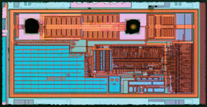
Break Microcontroller PIC12F617 Binary
We can Break Microcontroller PIC12F617 Binary, please view the Microcontroller PIC12F617 features for your reference:
High-Performance RISC CPU:
· Only 35 Instructions to Learn:
– All single-cycle instructions except branches
· Operating Speed:
– DC – 20 MHz oscillator/clock input
– DC – 200 ns instruction cycle
· Interrupt Capability
· 8-Level Deep Hardware Stack
· Direct, Indirect and Relative Addressing modes
Special Microcontroller Features:
· Precision Internal Oscillator:
– Factory calibrated to ±1%, typical
– Software selectable frequency: 4 MHz or 8 MHz
· Power-Saving Sleep mode
· Voltage Range:
– PIC12F609/615/617: 2.0V to 5.5V
– PIC12HV609/615: 2.0V to user defined maximum (see note)
· Industrial and Extended Temperature Range
· Power-on Reset (POR)
· Power-up Timer (PWRT) and Oscillator Start-up Timer (OST)
· Brown-out Reset (BOR)
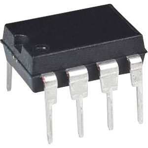
마이크로프로세서 PIC12F617 잠금 비트를 크래킹한 후 보안 플래시 메모리에서 암호화된 MCU PIC12F617 플래시 메모리 바이너리를 복원하고 PIC12F617 잠금 마이크로컨트롤러를 새 장치로 복제합니다.
· Watchdog Timer (WDT) with independent Oscillator for Reliable Operation after Break Microcontroller
· Multiplexed Master Clear with Pull-up/Input Pin
· Programmable Code Protection
· High Endurance Flash:
– 100,000 write Flash endurance
– Flash retention: > 40 years
· Self Read/ Write Program Memory (PIC12F617 only)
Low-Power Features:
· Standby Current:
– 50 nA @ 2.0V, typical
· Operating Current:
– 11 mA @ 32 kHz, 2.0V, typical
260 mA @ 4 MHz, 2.0V, typical
· Watchdog Timer Current:
– 1 mA @ 2.0V, typical
Peripheral Features:
· Shunt Voltage Regulator (PIC12HV609/615 only):
– 5 volt regulation
– 4 mA to 50 mA shunt range
· 5 I/O Pins and 1 Input Only
· High Current Source/Sink for Direct LED Drive when Break IC
– Interrupt-on-pin change or pins
– Individually programmable weak pull-ups
· Analog Comparator module with:
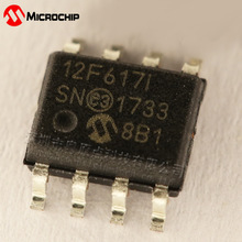
Copiar Microcontrolador Bloqueado PIC12F617 Flash O programa precisa quebrar a proteção sobre a memória flash MCU PIC12F617 segura e, em seguida, extrair o arquivo heximal incorporado do processador PIC12F617;
– One analog comparator
– Programmable on-chip voltage reference (CVREF) module (% of VDD)
– Comparator inputs and output externally accessible
– Built-In Hysteresis (software selectable)
· Timer0: 8-Bit Timer/Counter with 8-Bit Programmable Prescaler
· Enhanced Timer1:
– 16-bit timer/counter with prescaler
– External Timer1 Gate (count enable)
– Option to use OSC1 and OSC2 in LP mode as Timer1 oscillator if INTOSC mode selected
– Option to use system clock as Timer1
· In-Circuit Serial ProgrammingTM (ICSPTM) via Two Pins
PIC12F615/617/HV615 ONLY:
· Enhanced Capture, Compare, PWM module:
– 16-bit Capture, max. resolution 12.5 ns
– Compare, max. resolution 200 ns
– 10-bit PWM with 1 or 2 output channels, 1 output channel programmable “dead time,” max. frequency 20 kHz, auto-shutdown
· A/D Converter:
– 10-bit resolution and 4 channels, samples internal voltage references
· Timer2: 8-Bit Timer/Counter with 8-Bit Period Register, Prescaler and Postscaler
Posted in Break IC |
Tags: microcontroller break embedded archive, microcontroller break embedded code, microcontroller break embedded dump, microcontroller break embedded eeprom, microcontroller break embedded firmware, microcontroller break embedded information, microcontroller break embedded memory, microcontroller break embedded program |
Comments Closed
Break IC PIC16F627 Code
Break IC PIC16F627 and extract flash code from mcu pic16f627, the fuse bit of microcontroller pic16f627 will be cracked by focus ion beam;
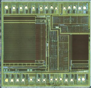
We can Break IC PIC16F627 Code, please view the IC PIC16F627 features for your reference:
High Performance RISC CPU:
· Only 35 instructions to learn
· All single-cycle instructions (200 ns), except for program branches which are two-cycle
· Operating speed:
– DC – 20 MHz clock input
– DC – 200 ns instruction cycle Interrupt capability
16 special function hardware registers
8-level deep hardware stack
Direct, Indirect and Relative addressing modes
Peripheral Features:
· 15 I/O pins with individual direction control
· High current sink/source for direct LED drive
· Analog comparator module with:
– Two analog comparators
– Programmable on-chip voltage reference (VREF) module
– Programmable input multiplexing from device inputs and internal voltage reference
– Comparator outputs are externally accessible
· Timer0: 8-bit timer/counter with 8-bit programmable prescaler
· Timer1: 16-bit timer/counter with external crystal/ clock capability
· Timer2: 8-bit timer/counter with 8-bit period register, prescaler and postscaler
· Capture, Compare, PWM (CCP) module
– Capture is 16-bit, max. resolution is 12.5 ns
– Compare is 16-bit, max. resolution is 200 ns
– PWM max. resolution is 10-bit
· Universal Synchronous/Asynchronous Receiver/Transmitter USART/SCI
· 16 Bytes of common RAM
Special Microcontroller Features:
· Power-on Reset (POR)
· Power-up Timer (PWRT) and Oscillator Start-up Timer (OST)
· Brown-out Detect (BOD)
· Watchdog Timer (WDT) with its own on-chip RC oscillator for reliable operation
· Multiplexed MCLR-pin
· Programmable weak pull-ups on PORTB
· Programmable code protection
· Low voltage programming
· Power saving SLEEP mode
· Selectable oscillator options
– FLASH configuration bits for oscillator options
– ER (External Resistor) oscillator
– Reduced part count
– Dual speed INTRC
– Lower current consumption
– EC External Clock input
– XT oscillator mode
– HS oscillator mode
– LP oscillator mode
· Serial in-circuit programming (via two pins)
· Four user programmable ID locations
CMOS Technology:
· Low-power, high-speed CMOS FLASH technology
· Fully static design
· Wide operating voltage range
– PIC16F627 – 3.0V to 5.5V
– PIC16F628 – 3.0V to 5.5V
– PIC16LF627 – 2.0V to 5.5V
– PIC16LF628 – 2.0V to 5.5V
· Commercial, industrial and extended temperature range
· Low power consumption
– < 2.0 mA @ 5.0V, 4.0 MHz
– 15 µA typical @ 3.0V, 32 kHz
– < 1.0 µA typical standby current @ 3.0V
Break ic flash ATMEGA461P Flash
We can Break ic flash ATMEGA461P Flash, please view the IC ATMEGA461P features for your reference:
The SPI Data Register is a read/write register used for data transfer between the Register File and the SPI Shift Register. Writing to the register initiates data transmission when Break ic flash.
Reading the register causes the Shift Register Receive buffer to be read. There are four combinations of SCK phase and polarity with respect to serial data, which are determined by control bits CPHA and CPOL. The SPI data transfer formats are shown in Figure 81 and Figure 82 if Break ic flash.
Data bits are shifted out and latched in on opposite edges of the SCK signal, ensuring sufficient time for data signals to stabilize. This is clearly seen by summarizing Table 94 and Table 95, as done below before Break ic flash:
The Universal Synchronous and Asynchronous serial Receiver and Transmitter (USART) is a highly flexible serial communication device. The main features are:
Full Duplex Operation (Independent Serial Receive and Transmit Registers)
Asynchronous or Synchronous Operation
Master or Slave Clocked Synchronous Operation
High Resolution Baud Rate Generator
Supports Serial Frames with 5, 6, 7, 8, or 9 Data Bits and 1 or 2 Stop Bits
Odd or Even Parity Generation and Parity Check Supported by Hardware if Break ic flash
Data OverRun Detection
Framing Error Detection
Noise Filtering Includes False Start Bit Detection and Digital Low Pass Filter
Three Separate Interrupts on TX Complete, TX Data Register Empty and RX Complete
Multi-processor Communication Mode
Double Speed Asynchronous Communication ModeThe ATmega461p has four USART’s, USART0, USART1, USART2, and USART3. The functionality for all four USART’s is described below Break ic flash.
USART0, USART1, USART2, and USART3 have different I/O registers as shown in “Register Summary” on page 385.
A simplified block diagram of the USART Transmitter is shown in Figure 83 on page after Break ic flash
CPU accessible I/O Registers and I/O pins are shown in bold.
The Power Reducion USART0 bit, PRUSART0, in “Power Reduction Register 0 PRR0” on page 54 must be disabled by writing a logical zero to it when Break ic flash.
The Power Reducion USART1 bit, PRUSART1, in “Power Reduction Register 1 – PRR1” on page 55 must be disabled by writing a logical zero to it.
The Power Reducion USART2 bit, PRUSART2, in “Power Reduction Register 1 – PRR1” on page 55 must be disabled by writing a logical zero to it if Break ic flash.
The Power Reducion USART3 bit, PRUSART3, in “Power Reduction Register 1 – PRR1” on page 55 must be disabled by writing a logical zero to it.