Archive for the ‘Break IC’ Category
 Break Microcontroller ATmega164PV Code
 November 24th, 2010 |
  Author:
 The ATmega164PV microcontroller has been widely adopted in long-life electronic products that require stable performance, efficient power usage, and dependable control capability. This device is commonly integrated into industrial automation equipment, smart control modules, instrumentation platforms, medical electronics, communication interfaces, environmental monitoring devices, and consumer products. Its architecture supports flexible embedded application development while storing operational firmware, configuration data, and application program functions within internal flash, eeprom, and non-volatile memory resources. In many commercial deployments, manufacturers implement protective, protected, locked, secured, or encrypted configurations to preserve proprietary design assets and reduce unauthorized duplication. As products age and original development records become unavailable, recovering historical binary, heximal, source code, or archived engineering files becomes increasingly important for maintenance and lifecycle continuity.
The frequency ranges are preliminary values. Actual values are TBD.
This option should not be used with crystals, only with ceramic resonators.
Our “Break Microcontroller ATmega164PV Code” service is designed for authorized recovery and reconstruction of valuable engineering assets from existing embedded hardware. The objective is not to compromise active products but to help customers retrieve historical firmware, reconstruct lost program structures, and preserve inaccessible technical documentation. Through structured laboratory workflows and device evaluation processes, our team supports projects involving memory assessment, data recovery, and high-level decode of historical firmware structures.
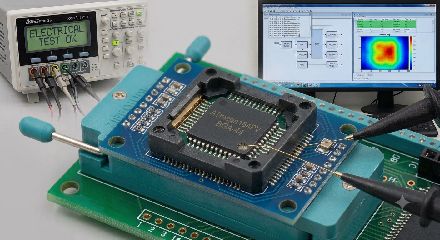
Depending on project scope and authorization, controlled inspection methods may be used to evaluate storage organization and recover available binary and heximal records from internal flash and eeprom regions. Extracted information is reorganized into engineering-ready file and archive outputs that assist customers in maintaining legacy systems, preparing controlled clone references, validating compatibility, or supporting limited duplicate production programs.
These options are intended for use with ceramic resonators and will ensure frequency stability at start-up. They can also be used with crystals when not operating close to the maximum frequency of the device, and if frequency stability at start-up is not important for the application.
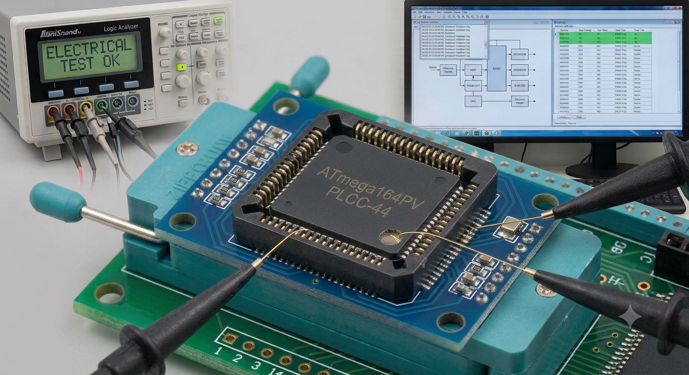
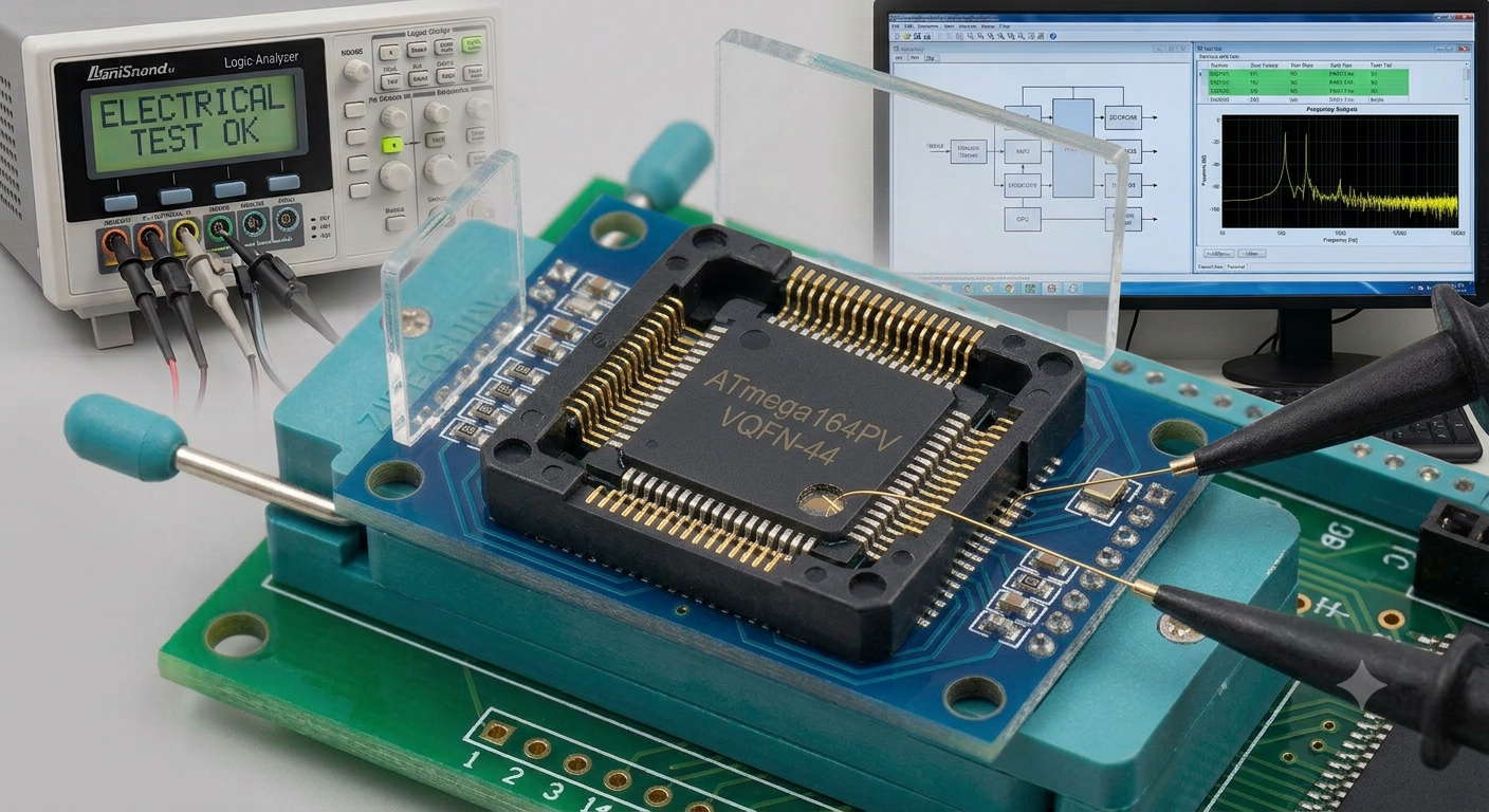
The technical workflow combines preservation methodology with disciplined engineering analysis. Device behavior is documented and internal structures are evaluated to reconstruct meaningful source code references and recover operational firmware relationships. Specialized analysis may support interpretation of archived data and reconstruction of historical program logic while preserving consistency with the original hardware environment. Where appropriate and legally authorized, controlled package examination and limited decapsulate procedures may assist interpretation of inaccessible memory structures and organization of recovered binary files. Rather than attempting to attack, break, or hack active security controls, the process prioritizes controlled recovery, validation, and documentation of engineering assets. Structured decode procedures help transform fragmented archives into usable outputs that support product continuity and long-term technical management.
This Crystal Oscillator is a full swing oscillator, with rail-to-rail swing on the XTAL2 output. This is useful for driving other clock inputs and in noisy environments. The current consumption is higher than the “Low Power Crystal Oscillator” on page 41. Note that the Full Swing Crystal Oscillator will only operate for Vcc = 2.7 – 5.5 volts.
C1 and C2 should always be equal for both crystals and resonators. The optimal value of the capacitors depends on the crystal or resonator in use, the amount of stray capacitance, and the electromagnetic noise of the environment. Some initial guidelines for choosing capacitors for use with crystals are given in Table 12. For ceramic resonators, the capacitor values given by the manufacturer should be used.
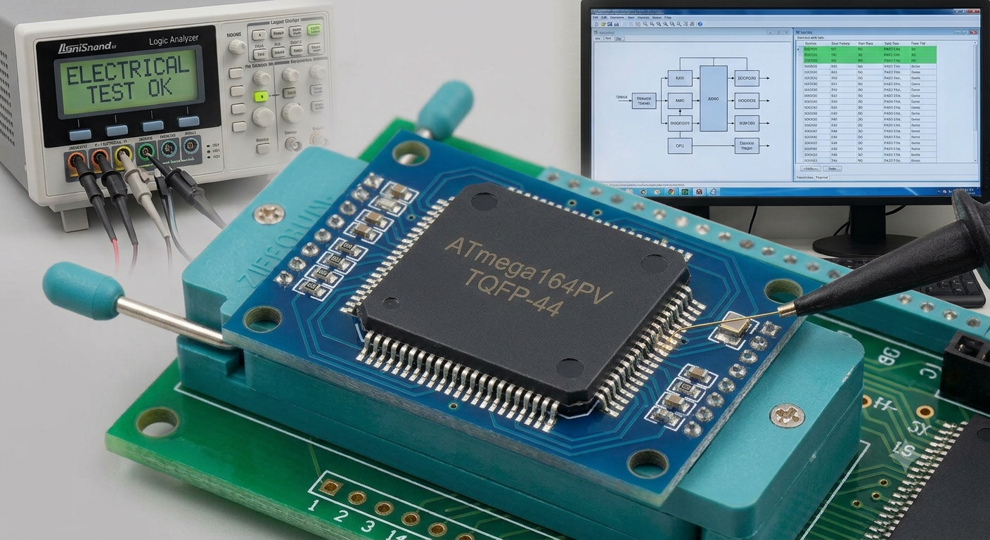
If 8 MHz frequency exceeds the specification of the device (depends on VCC), the CKDIV8 Fuse can be programmed in order to divide the internal frequency by 8. It must be ensured that the resulting divided clock meets the frequency specification of the device. These options should only be used when not operating close to the maximum frequency of the device, and only if frequency stability at start-up is not important for the application. These options are not suitable for crystals. These options are intended for use with ceramic resonators and will ensure frequency stability at start-up. They can also be used with crystals when not operating close to the maximum frequency of the device, and if frequency stability at start-up is not important for the application.
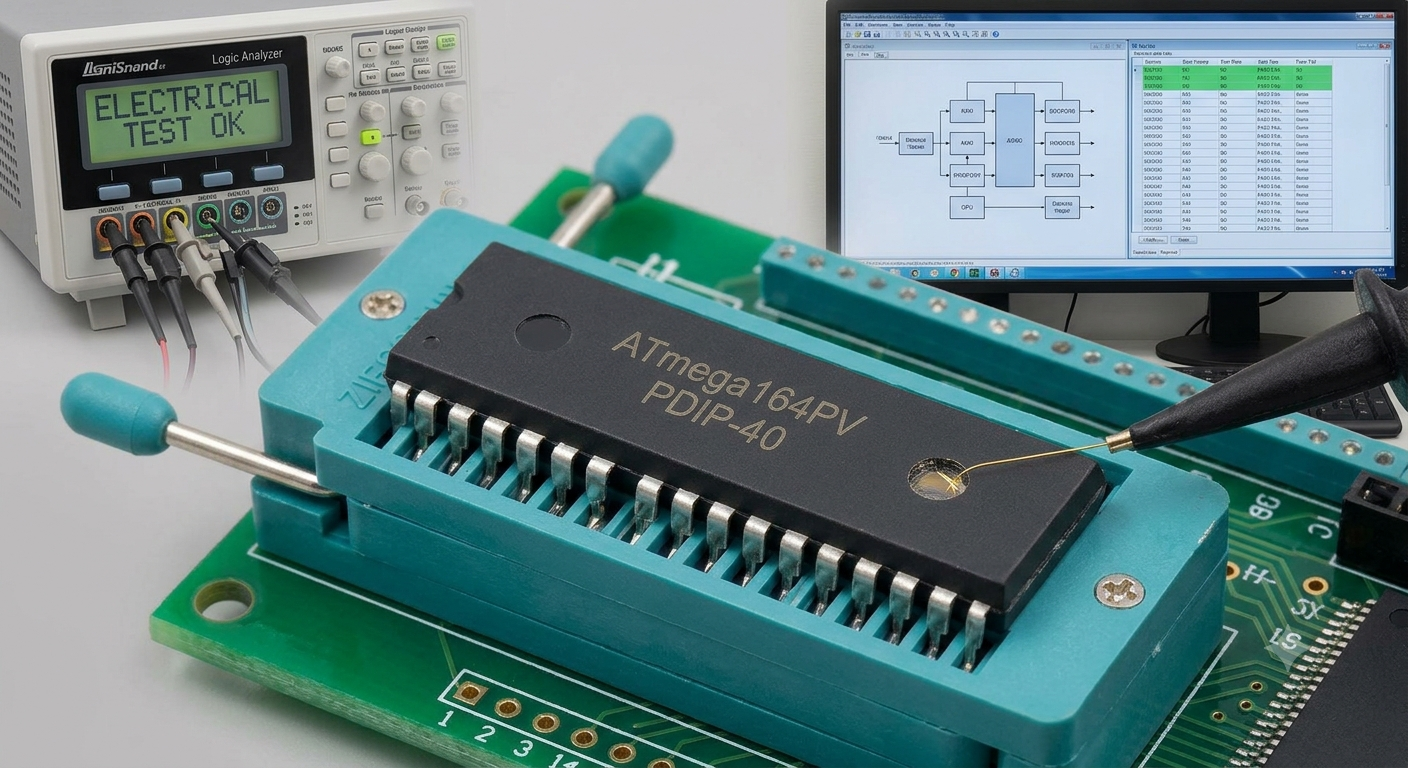
For end users, recovering ATmega164PV code can significantly reduce redevelopment effort and preserve proven designs already deployed in the field. Access to historical firmware, organized data archives, and reconstructed source code enables maintenance teams to support existing installations, modernize platforms, and extend product service life. Engineering groups can reuse validated program behavior, document historical architecture, and maintain operational compatibility without restarting development from the beginning. By combining embedded expertise with responsible recovery practices, our service helps customers transform inaccessible device content into reusable engineering knowledge and maintain continuity across critical electronic systems.
Break Microcontroller ATmega164 Code
Break Microcontroller ATmega164 flash memory and extract ATmega164 MCU code from its secured memory, make ATmega164 processor cloning;
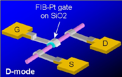
With all the features the External Memory Interface provides, it is well suited to operate as an interface to memory devices such as External SRAM and Flash, and peripherals such as LCD-display, A/D, and D/A. The main features are:
Four different wait-state settings (including no wait-state).
Independent wait-state setting for different extErnal Memory sectors (configurable sector size).
The number of bits dedicated to address high byte is selectable.
Bus keepers on data lines to minimize current consumption (optional) if recover mcu atmega2560 flash.
When the eXternal MEMory (XMEM) is enabled, address space outside the internal SRAM becomes available using the dedicated External Memory pins (see Figure 2 on page 3, Table 36 on page 88, Table 42 on page 92, and Table 54 on page 102). The memory configuration is shown in Figure 14.
The interface consists of: AD7:0: Multiplexed low-order address bus and data bus.
A15:8: High-order address bus (configurable number of bits).
ALE: Address latch enable.
RD: Read strobe.
WR: Write strobe.
The control bits for the External Memory Interface are located in two registers, the External Memory Control Register A – XMCRA, and the External Memory Control Register B– XMCRB.
When the XMEM interface is enabled, the XMEM interface will override the setting in the data direction registers that corresponds to the ports dedicated to the XMEM interface.
For details about the port override, see the alternate functions in section “I/O-Ports” on page 81. The XMEM interface will auto-detect whether an access is internal or external if reverse engineering microcontroller atmega1281 program.
If the access is external, the XMEM interface will output address, data, and the control signals on the ports according to Figure 16 (this figure shows the wave forms without wait-states). When ALE goes from high-to-low, there is a valid address on AD7:0. ALE is low during a data transfer.
When the XMEM interface is enabled, also an internal access will cause activity on address, data and ALE ports, but the RD and WR strobes will not toggle during internal access. When the External Memory Interface is disabled, the normal pin and data direction settings are used.
Note that when the XMEM interface is disabled, the address space above the internal SRAM boundary is not mapped into the internal SRAM. Figure 15 illustrates how to connect an external SRAM to the AVR using an octal latch (typically “74 x 573” or equivalent) which is transparent when G is high.
Due to the high-speed operation of the XRAM interface, the address latch must be selected with care for system frequencies above 8 MHz @ 4V and 4 MHz @ 2.7V.
When operating at conditions above these frequencies, the typical old style 74HC series latch becomes inadequate. The External Memory Interface is designed in compliance to the 74AHC series latch. However, most latches can be used as long they comply with the main timing parameters. The main parameters for the address latch are:
D to Q propagation delay (tPD).
Data setup time before G low (tSU).
Data (address) hold time after G low (TH).
The External Memory Interface is designed to guaranty minimum address hold time after G is asserted low of th = 5 ns. Refer to tLAXX_LD/tLLAXX_ST in “External Data Memory Timing” Tables 169 through Tables 176 on pages 376 – 378.
The D-to-Q propagation delay (tPD) must be taken into consideration when calculating the access time requirement of the external component. The data setup time before G low (tSU) must not exceed address valid to ALE low (tAVLLC) minus PCB wiring delay (dependent on the capacitive load).
The pull-ups on the AD7:0 ports may be activated if the corresponding Port register is written to one. To reduce power consumption in sleep mode, it is recommended to disable the pull-ups by writing the Port register to zero before entering sleep.
The XMEM interface also provides a bus-keeper on the AD7:0 lines. The bus-keeper can be disabled and enabled in software as described in “External Memory Control Register B – XMCRB” on page 35. When enabled, the bus-keeper will keep the previous value on the AD7:0 bus while these lines are tri-stated by the XMEM interface.
 Posted in Break IC |
  Tags: break microcontroller embedded archive, break microcontroller embedded bin, break microcontroller embedded code, break microcontroller embedded content, break microcontroller embedded data, break microcontroller embedded eeprom, break microcontroller embedded file, break microcontroller embedded firmware, break microcontroller embedded hex, break microcontroller embedded information, break microcontroller embedded memory, break microcontroller embedded program |
  Comments Closed
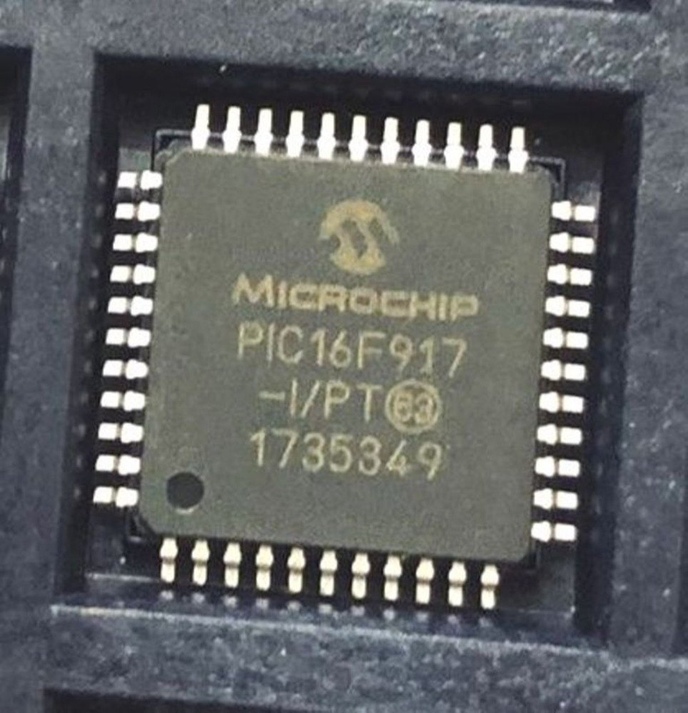
Break IC PIC16F917 Heximal
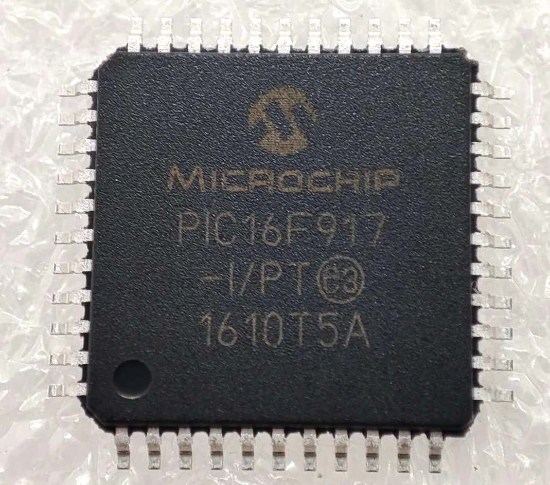
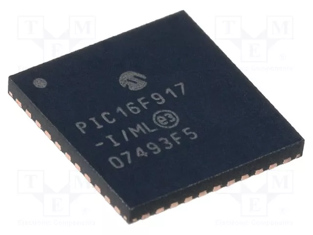
The PIC16F917 is a versatile microcontroller widely integrated into modern embedded electronic systems requiring reliable control, compact architecture, and low-power operation. This IC is commonly deployed in industrial instrumentation, automotive electronics, smart metering equipment, consumer appliances, and medical monitoring devices. Its integrated peripherals and onboard memory architecture allow manufacturers to store complex firmware, operational program logic, and critical data directly inside the chip. In many commercial applications, these internal resources are intentionally protected, locked, and sometimes encrypted to prevent unauthorized access to the original source code, binary, or heximal file archive. While this security is important for intellectual property protection, it can also create serious obstacles when systems require maintenance, duplication, or redevelopment years later.
The external Resistor-Capacitor (RC) modes support the use of an external RC circuit. This allows the designer maximum flexibility in frequency choice while keeping costs to a minimum when clock accuracy is not required. There are two modes: RC and RCIO.
In RC mode, the RC circuit connects to OSC1. OSC2/CLKOUT outputs the RC oscillator frequency divided by 4. This signal may be used to provide a clock for external circuitry, synchronization, calibration, test or other application requirements. Figure 4-5 shows the external RC mode connections. The INTOSC and INTOSCIO modes configure the internal oscillators as the system clock source when (SCS) bit of the OSCCON register. user-adjusted via software using the OSCTUNE register (Register 4-2).
2. The LFINTOSC (Low-Frequency Internal Oscillator) is uncalibrated and operates at 31 kHz. The system clock speed can be selected via software.
INTERNAL CLOCK MODEL
The Oscillator module has two independent, internal oscillators that can be configured or selected as the system clock source.
1. The HFINTOSC (High-Frequency Internal Oscillator) is factory calibrated and operates at 8 MHz. The frequency of the HFINTOSC can be user-adjusted via software using the OSCTUNE register (Register 4-2).
2. The LFINTOSC (Low-Frequency Internal Oscillator) is uncalibrated and operates at 31 kHz. The system clock speed can be selected via software using the Internal Oscillator Frequency Select bits IRCF<2:0> of the OSCCON register. an> The INTOSC and INTOSCIO modes configure the internal oscillators as the system clock source when bit of the OSCCON register. See Section 4.6 user-adjusted via software using the OSCTUNE register (Register 4-2).
2. The LFINTOSC (Low-Frequency Internal Oscillator) is uncalibrated and operates at 31 kHz. The system clock speed can be selected via software.
Our “Break IC PIC16F917 Heximal” service is specifically developed to attack, break, and decode highly secured microcontrollers while preserving the integrity of the internal data structure. By combining advanced decapsulate methods with precision electronic analysis, our engineering team can retrieve hidden firmware, extract complete binary and heximal files, and reconstruct the original source code from internal flash, EEPROM, and embedded memory regions. Even when the device contains sophisticated protective mechanisms or encrypted storage configurations, we apply specialized techniques to effectively hack through these barriers and obtain a usable archive of the original program. The recovered information can then be utilized to clone, duplicate, repair, or migrate legacy systems into updated hardware environments without losing functionality or compatibility.
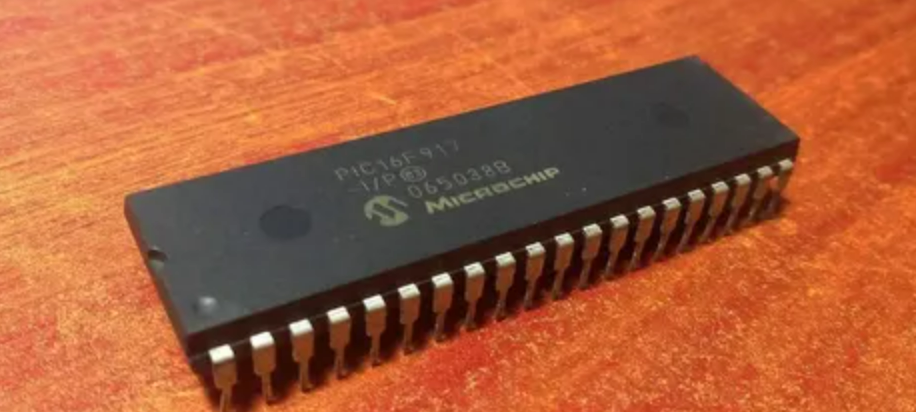
Technically, the recovery workflow involves several layers of analysis. The first stage often includes controlled decapsulation, exposing the silicon die for direct interaction with internal circuitry. This enables accurate retrieval of low-level embedded data from protected memory cells. Once the raw binary or heximal dump has been collected, proprietary decode algorithms are used to organize fragmented files into structured firmware archives. This process allows the original program logic and operational sequences to be reconstructed with high precision. In addition, our engineers verify the integrity of each extracted data file, ensuring the resulting source code accurately reflects the behavior of the original PIC16F917 IC. Through this combination of physical analysis and logical reconstruction, we are able to overcome many forms of locked and secured firmware protection.
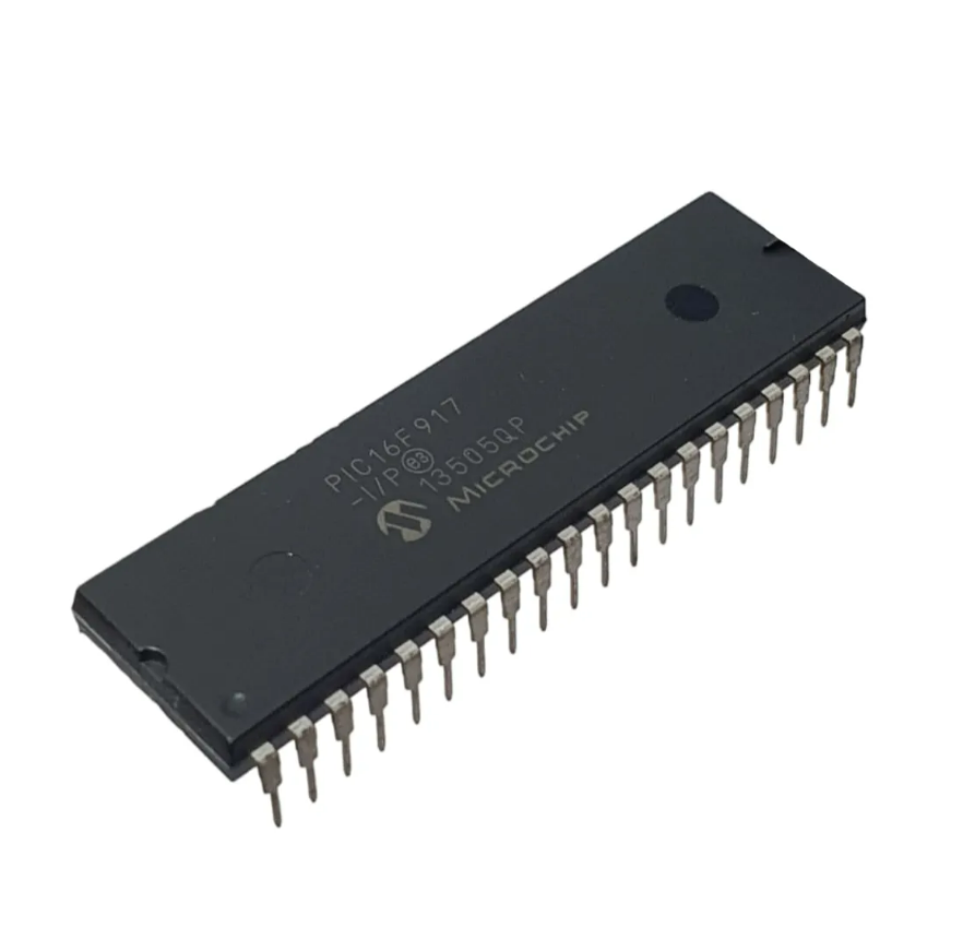
For end users, the advantages of recovering PIC16F917 firmware and heximal data are substantial. Manufacturers facing discontinued components, missing development documentation, or supply chain shortages can regain complete access to critical embedded assets without redesigning an entire system. By using our service to attack, decode, and recover protected memory, customers can preserve legacy equipment, accelerate product maintenance, and efficiently duplicate proven designs. Whether the objective is long-term product support, reverse engineering research, or rapid redevelopment, our capability to break and reconstruct PIC16F917 binary archives provides a dependable solution for unlocking valuable electronic intellectual property.
Break Microcontroller ATmega461A Firmware
The ATmega461A microcontroller is a high-performance, low-power 8-bit AVR RISC-based device widely relied upon in advanced battery charging systems, motor control peripherals, handheld power tools, and localized industrial sensor hubs. A standout feature of this chip is its highly flexible Pulse Width Modulation (PWM) channels paired with a high-speed Analog-to-Digital Converter, making it uniquely suited for precise analog regulation and high-frequency power management tasks. The core operating logic that directs these hardware operations runs silently as an embedded program within the chip’s internal structure. However, original equipment manufacturers frequently face critical production bottlenecks when a field system requires legacy optimization, but the development archives, original source code, or compiling records have been lost over time. When a component supplier disappears or a system faces immediate obsolescence, finding a reliable engineering path to extract the software becomes an absolute necessity. Our advanced laboratory specializes in precise engineering extractions designed to break microcontroller atmega461a firmware configurations, ensuring your business reclaims full operational access to its hardware investments.
The ATMEGA461A is a complex microcontroller with more peripheral units than can be supported within the 64 location reserved in the Opcode for the IN and OUT instructions.
For the Extended I/O space from $060 – $1FF in SRAM, only the ST/STS/STD and LD/LDS/LDD instructions can be used. The first 4,608/8,704 Data Memory locations address both the Register File, the I/O Memory, Extended I/O Memory, and the internal data SRAM. The first 32 locations address the Register file, the next 64 location the standard I/O Memory, then 416 locations of Extended I/O memory and the next 8,192 locations address the internal data SRAM. An optional external data SRAM can be used with the ATmega461. This SRAM will occupy an area in the remaining address locations in the 64K address space. This area starts at the address following the internal SRAM.
The Register file, I/O, Extended I/O and Internal SRAM occupies the lowest 4,608/8,704 bytes, so when using 64KB (65,536 bytes) of External Memory, 60,478/56,832 Bytes of External Memory are available. See “External Memory Interface” on page 29 for details on how to take advantage of the external memory map. When the addresses accessing the SRAM memory space exceeds the internal data memory locations, the external data SRAM is accessed using the same instructions as for the internal data memory access. When the internal data memories are accessed, the break and write strobe pins (PG0 and PG1) are inactive during the whole access cycle.
External SRAM operation is enabled by setting the SRE bit in the XMCRA Register. Accessing external SRAM takes one additional clock cycle per byte compared to access of the internal SRAM. This means that the commands LD, ST, LDS, STS, LDD, STD, PUSH, and POP take one additional clock cycle. If the Stack is placed in external SRAM, interrupts, subroutine calls and returns take three clock cycles extra because the three-byte program counter is pushed and popped, and external memory access does not take advantage of the internal pipe-line memory access.
When external SRAM interface is used with wait-state, one-byte external access takes two, three, or four additional clock cycles for one, two, and three wait-states respectively. Interrupts, subroutine calls and returns will need five, seven, or nine clock cycles more than specified in the instruction set manual for one, two, and three wait-states. The five different addressing modes for the data memory cover: Direct, Indirect with Displacement, Indirect, Indirect with Pre-decrement, and Indirect with Post-increment. In the Register file, registers R26 to R31 feature the indirect addressing pointer registers. The direct addressing reaches the entire data space. The Indirect with Displacement mode reaches 63 address locations from the base address given by the Y- or Z-register. When using register indirect addressing modes with automatic pre-decrement and post increment, the address registers X, Y, and Z are decremented or incremented.
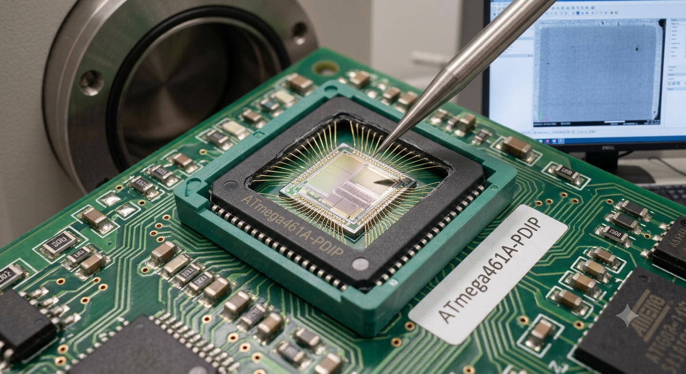
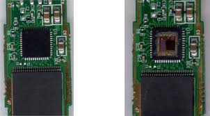
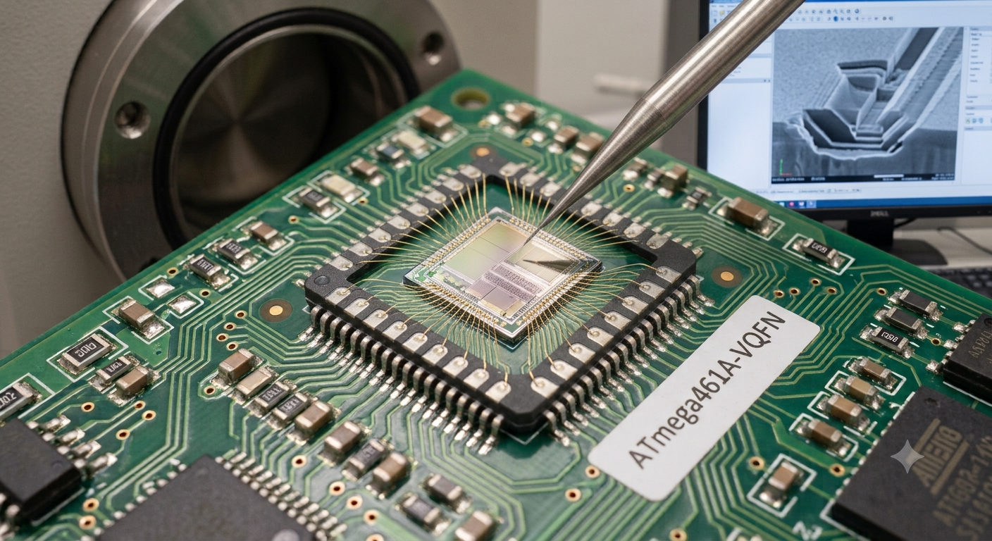
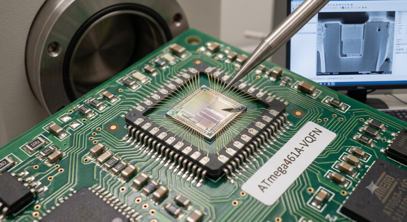
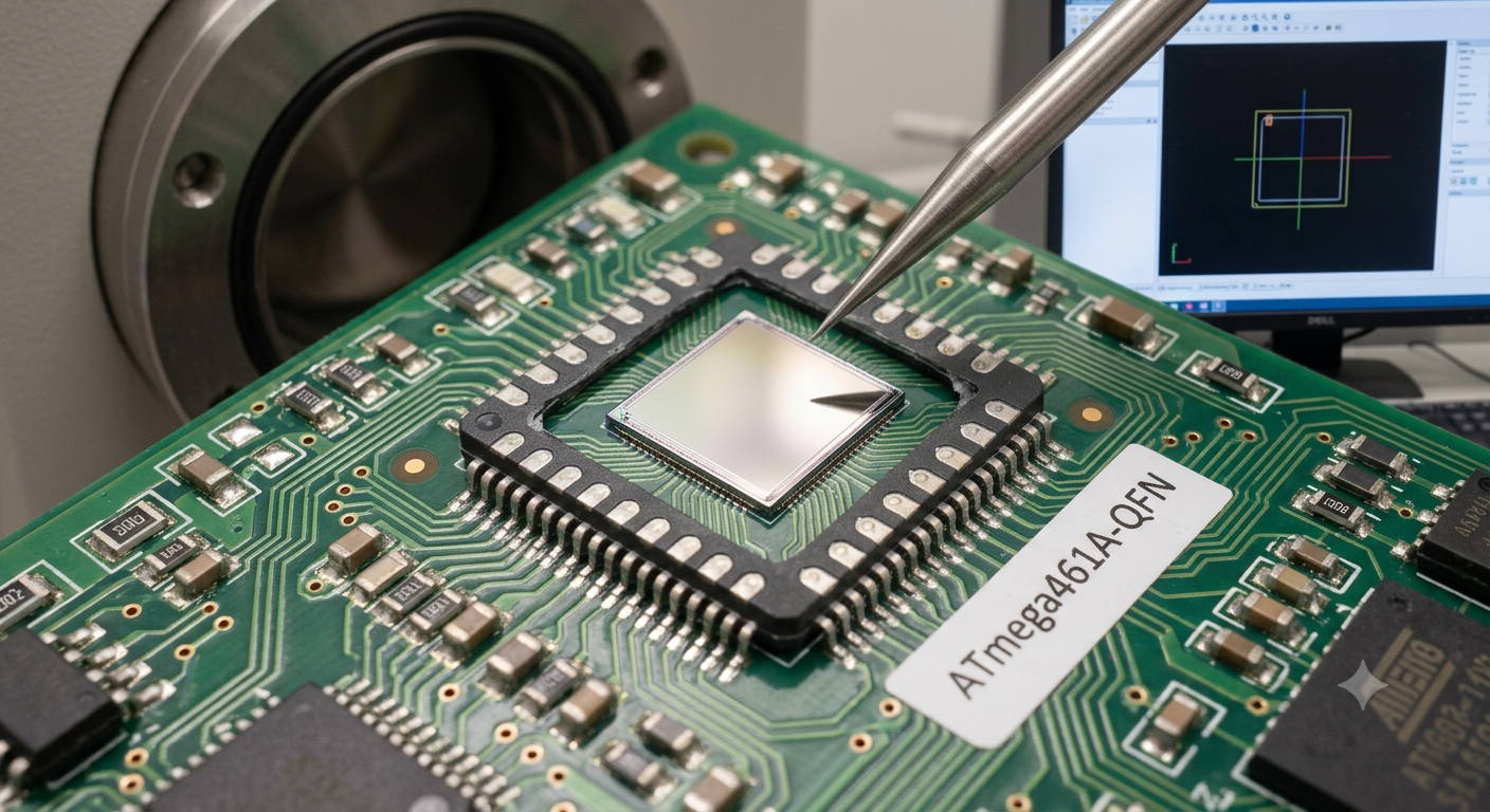
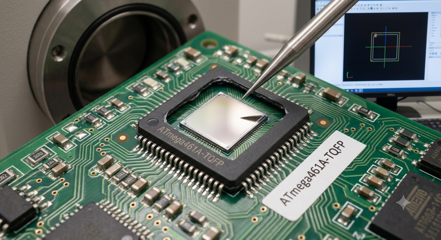
Accessing the machine instructions stored inside a secured or locked integrated circuit requires navigating dense physical and electrical defense systems designed to prevent unauthorized readout. To systematically attack, break, and decode these embedded protection mechanisms, our micro-electronics laboratory utilizes a non-destructive, highly controlled physical process. Technicians first decapsulate the outer protective plastic housing of the device using precise chemical etching to expose the raw silicon micro-die underneath. Once the internal circuitry is completely visible under high-power microscopy, we deploy specialized fault-injection and micro-probing equipment to target the protective code fuses and lock bits. By temporarily manipulating internal voltage levels or modifying configuration paths directly on the silicon substrate, our team can safely bypass the chip’s reading restrictions without destroying the underlying hardware. This allows us to smoothly retrieve the tightly guarded firmware, raw data, and structural configurations straight from the inner flash and internal eeprom memory sectors, compiling the extracted information into a flawless, uncorrupted heximal file that mirrors the original application instructions perfectly.
Eliminating Obsolescence Risks Through Precision Device Cloning
The underlying purpose of choosing to hack, duplicate, or extract code from a protected microcontroller is to insulate an enterprise from single-point supply chain failures and eliminate the massive costs of a ground-up software rewrite. When access to an active product file or software archive is severed, engineering teams use our advanced recovery services to salvage the vital logic required to clone the hardware’s exact operational profile. Whether the proprietary routines are held entirely in the main chip memory or distributed across peripheral PLD blocks, our custom extraction tools pull every byte of information safely. Once our team successfully extracts the raw data stream, developers gain the immediate capability to duplicate the system behavior onto a modern, readily available replacement microcontroller. This comprehensive recovery ensures you can maintain absolute system continuity, compile a fresh software backup, and confidently manufacture drop-in replacement boards without experiencing unexpected field downtime or production halts.
Strategic Capital Protection and Operational Benefits for the End User
Partnering with an experienced engineering team to unlock and recover embedded software gives product managers, system integrators, and maintenance engineers an immense technical and financial advantage. Instead of dedicating months of expensive R&D time to manually reverse-engineer and re-code a complex application from scratch—a risky process that notoriously introduces hidden programming bugs—our laboratory provides an efficient pipeline to a fully verified, operational firmware file. This absolute structural continuity guarantees that every newly generated duplicate circuit board performs identically to the field-proven units your customers already trust. By utilizing our custom microcontroller extraction services, your business effectively mitigates the existential risks of parts obsolescence, safeguards vital corporate intellectual property, and secures a completely predictable, stable roadmap for your industrial hardware investments for many years to come.
Break IC PIC16F914 Heximal
The PIC16F914 microcontroller is widely used in industrial control systems, medical instruments, automotive electronics, smart metering devices, household appliances, and embedded automation products because of its low power consumption, stable performance, integrated LCD control capability, and flexible peripheral architecture. As many manufacturers rely on this MCU to operate proprietary equipment, the firmware, flash memory, EEPROM data, and embedded program archive stored inside the chip often become critical business assets.
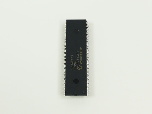
However, when the original developer disappears, production documentation is lost, or a secured and protected chip becomes locked or encrypted, companies may urgently need to retrieve binary files, recover source code references, or duplicate an existing MCU program for maintenance and continued production. Our “Break IC PIC16F914 Heximal” service is designed to help engineers, repair centers, and manufacturers restore valuable microcontroller data safely and efficiently while minimizing downtime and hardware replacement costs.
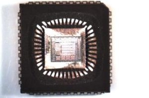
Low-Power Features:
· Standby Current:
– <100 nA @ 2.0V, typical
· Operating Current:
– 11 ìA @ 32 kHz, 2.0V, typical
– 220 ìA @ 4 MHz, 2.0V, typical
· Watchdog Timer Current:
– 1 ìA @ 2.0V, typical
Peripheral Features:
· Liquid Crystal Display module:
– Up to 60/96/168 pixel drive capability on 28/40/64-pin devices, respectively
– Four commons
· Up to 24/35/53 I/O pins and 1 input-only pin:
– High-current source/sink for direct LED drive
– Interrupt-on-change pin
– Individually programmable weak pull-ups
· In-Circuit Serial Programming™ (ICSP™) via two pins
· Analog comparator module with:
– Two analog comparators
– Programmable on-chip voltage reference (CVREF) module (% of VDD)
– Comparator inputs and outputs externally accessible
· A/D Converter:
– 10-bit resolution and up to 8 channels
· Timer0: 8-bit timer/counter with 8-bit programmable prescaler
· Enhanced Timer1:
– 16-bit timer/counter with prescaler
– External Timer1 Gate (count enable)
– Option to use OSC1 and OSC2 as Timer1 oscillator if INTOSCIO or LP mode is selected
· Timer2: 8-bit timer/counter with 8-bit period register, prescaler and postscaler
· Addressable Universal Synchronous Asynchronous Receiver Transmitter (AUSART)
· Up to 2 Capture, Compare, PWM modules:
– 16-bit Capture, max. resolution 12.5 ns
– 16-bit Compare, max. resolution 200 ns
– 10-bit PWM, max. frequency 20 kHz
· Synchronous Serial Port (SSP) with I2C™
Our engineering team specializes in advanced MCU attack and reverse analysis solutions for protected and secured embedded systems. Through professional hardware inspection, chip decapsulation, firmware extraction, and low-level memory analysis, we can help customers break locked protection structures and retrieve important flash, EEPROM, binary, heximal, and firmware archive data from damaged or encrypted IC devices.
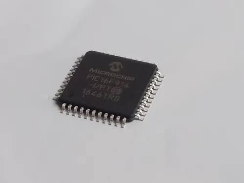
Depending on the protection level and physical condition of the MCU, our process may involve controlled voltage analysis, memory mapping, signal monitoring, decapsulate procedures, or customized decoding workflows to access secured program memory regions. Many clients require this service to clone obsolete industrial boards, duplicate unavailable spare modules, recover embedded source code references, or restore a lost production program file from a protected PIC16F914 MCU.
In some cases, companies also need to hack malfunctioning systems for diagnostic purposes, retrieve calibration data from locked EEPROM memory, or decode corrupted firmware archives to continue long-term equipment support. By combining hardware expertise with deep understanding of embedded architecture, we can attack difficult protection mechanisms while preserving original data integrity as much as possible.
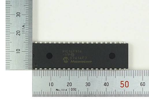
Unlike generic chip programming services, our work focuses on complex recovery situations involving encrypted or secured microcontrollers where the original binary or flash archive is no longer accessible through standard programming tools. The PIC16F914 is often found in industrial LCD control units, portable medical devices, automotive dashboards, HVAC controllers, and intelligent sensor modules, making firmware continuity extremely important for end users.
A lost MCU program can halt production lines, interrupt machine servicing, or force companies into expensive redesign projects. Our service helps customers retrieve protected firmware, clone unavailable control boards, duplicate embedded logic, and recover valuable operational data archives from damaged or locked IC components.
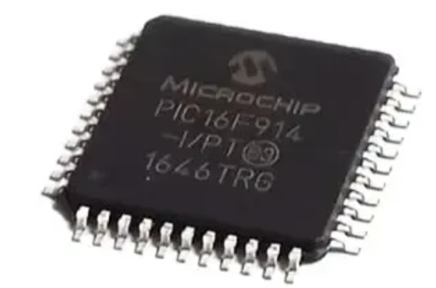
We also assist clients who need to compare firmware revisions, analyze legacy program structures, or restore embedded memory content from defective devices for compatibility testing and maintenance. These solutions are particularly valuable for factories operating aging equipment where replacement hardware is no longer manufactured.
With extensive experience handling protected and encrypted microcontrollers, we understand the importance of confidentiality, technical precision, and fast turnaround times. Every project involving PIC16F914 firmware retrieval, flash recovery, EEPROM extraction, or binary decoding is evaluated individually to determine the safest and most effective technical path. Whether the requirement is to break MCU protection, retrieve lost heximal files, clone embedded firmware, restore corrupted program archives, or decode secured memory structures, our service provides a reliable solution for companies that depend on continuous operation of critical electronic systems.
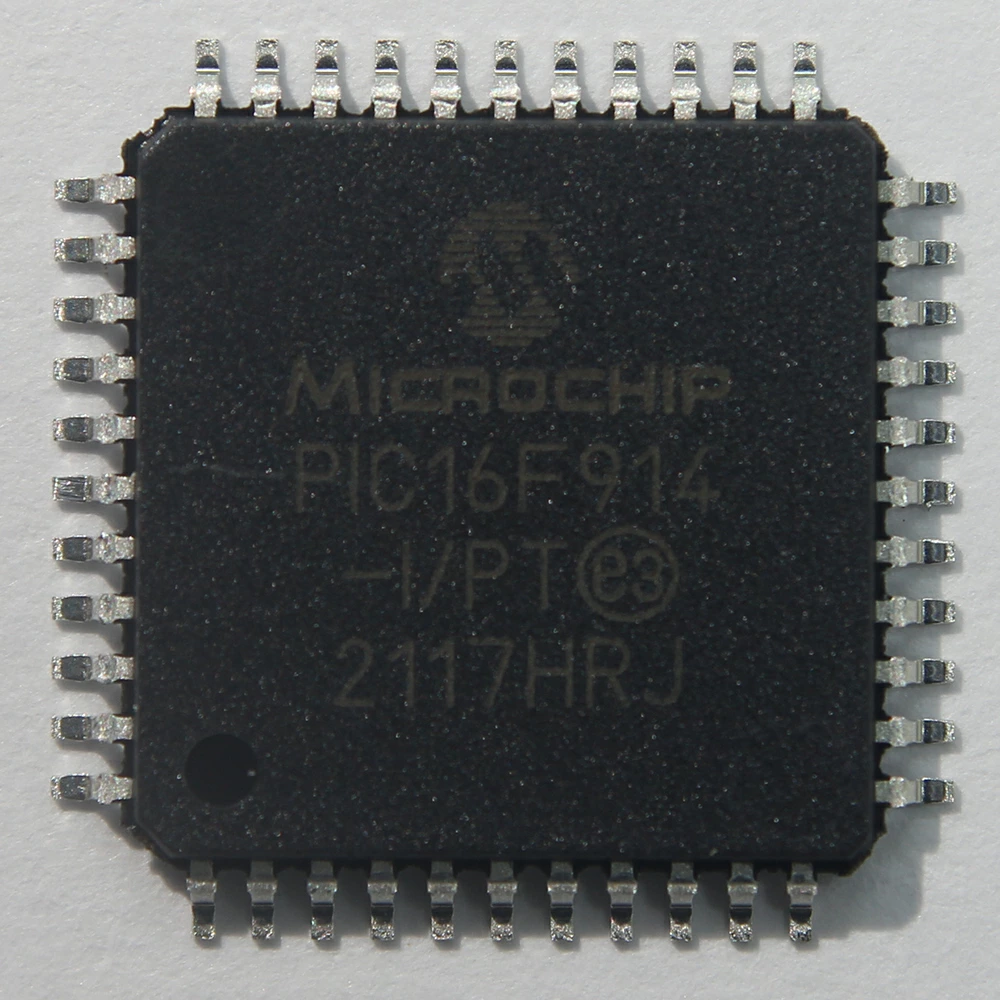
Break Chip PIC16F785 Heximal
Break Chip PIC16F785 and readout the Heximal content from MCU PIC16F785, the fuse bit of microcontroller PIC16F785 will be unlocked for opening status;
High-Performance RISC CPU:
· Only 35 Instructions to Learn:
– All single-cycle instructions except branches
· Operating Speed:
– DC – 20 MHz oscillator/clock input
– DC – 200 ns instruction cycle
· Interrupt Capability
· 8-Level Seep Hardware Stack
· Direct, Indirect and Relative Addressing modes
Special Microcontroller Features:
· Precision Internal Oscillator:
– Factory calibrated to ±1%
– Software selectable frequency range of 8 MHz to 32 kHz
– Software tunable
– Two-Speed Start-up mode
– Crystal fail detect for critical applications
– Clock mode switching during operation for power savings after recover mcu p89lpc925fdh hex
· Power-Saving Sleep mode
· Wide Operating Voltage Range (2.0V-5.5V)
· Industrial and Extended Temperature Range
· Power-on Reset (POR)
· Power-up Timer (PWRT) and Oscillator Start-up Timer (OST)
· Brown-out Reset (BOR) with Software Control Option
· Enhanced Low-Current Watchdog Timer (WDT) with on-chip Oscillator (software selectable nominal 268 seconds with full prescaler) with Software Enable
· Multiplexed Master Clear with Pull-up/Input Pin if break chip
· Programmable Code Protection
· High-Endurance Flash/EEPROM cell:
– 100,000 write Flash endurance
– 1,000,000 write EEPROM endurance
– Flash/Data EEPROM retention: > 40 years
Low-Power Features:
· Standby Current:
– 30 nA @ 2.0V, typical
· Operating Current:
– 8.5 ìA @ 32 kHz, 2.0V, typical
– 100 ìA @ 1 MHz, 2.0V, typical
· Watchdog Timer Current:
– 1 ìA @ 2.0V, typical
· Timer1 Oscillator Current:
– 2 ìA @ 32 kHz, 2.0V, typical
Peripheral Features:
· High-Speed Comparator module with:
– Two independent analog comparators
– Programmable on-chip voltage reference (CVREF) module (% of VDD) when break microcontroller pic12f629 program
– 1.2V band gap voltage reference
– Comparator inputs and outputs externally accessible
– < 40 ns propagation delay
– 2 mv offset, typical
· Operational Amplifier module with 2 independent Op Amps:
– 3 MHz GBWP, typical
– All I/O pins externally accessible
· Two-Phase Asynchronous Feedback PWM module:
– Complementary output with programmable dead band delay
– Infinite resolution analog duty cycle
– Sync Output/Input for multi-phase PWM
– FOSC/2 maximum PWM frequency
· A/D Converter:
– 10-bit resolution and 14 channels (2 internal)
· 17 I/O pins and 1 Input-only Pin:
– High-current source/sink for direct LED drive
– Interrupt-on-pin change
– Individually programmable weak pull-ups
· Timer0: 8-Bit Timer/Counter with 8-Bit Programmable Prescaler
· Enhanced Timer1:
– 16-bit timer/counter with prescaler
– External Gate Input mode
– Option to use OSC1 and OSC2 in LP mode as Timer1 oscillator, if INTOSC mode selected
· Timer2: 8-Bit Timer/Counter with 8-Bit Period Register, Prescaler and Postscaler for the purpose of break chip
· Capture, Compare, PWM module:
– 16-bit Capture, max resolution 12.5 ns
– Compare, max resolution 200 ns
– 10-bit PWM with 1 output channel, max frequency 20 kHz
· In-Circuit Serial ProgrammingTM (ICSPTM) via two pins
· Shunt Voltage Regulator (PIC16HV785 only):
– 5 volt regulation
– 4 mA to 50 mA shunt range
Break IC ATtiny88 Heximal
Break IC ATtiny88 flash and eeprom memory, then readout Heximal from MCU ATtiny88 program memory, unlock microcontroller attiny88 security fuse bit and extract the embedded firmware;
High Performance, Low Power AVR® 8-Bit Microcontroller
Advanced RISC Architecture
– 123 Powerful Instructions – Most Single Clock Cycle Execution
– 32 x 8 General Purpose Working Registers
– Fully Static Operation if reverse engineering microcontroller pic16c558a
High Endurance Non-volatile Memory Segments
– 4K/8K Bytes of In-System Self-Programmable Flash program memory(ATtiny48/88)
– 64/64 Bytes EEPROM (ATtiny48/88)
– 256/512 Bytes Internal SRAM (ATtiny48/88)
– Write/Erase Cycles: 10,000 Flash/100,000 EEPROM
– Data retention: 20 years at 85°C / 100 years at 25°C
– Programming Lock for Software Security
Peripheral Features
– One 8-bit Timer/Counter with Separate Prescaler and Compare Mode
– One 16-bit Timer/Counter with Prescaler, and Compare and Capture Modes
– 8-channel 10-bit ADC in 32-lead TQFP and 32-pad QFN/MLF package
– 6-channel 10-bit ADC in 28-pin PDIP and 28-pad QFN/MLF package
– Master/Slave SPI Serial Interface
– Byte-oriented 2-wire Serial Interface (Philips I2C Compatible)
– Programmable Watchdog Timer with Separate On-chip Oscillator
– On-chip Analog Comparator
– Interrupt and Wake-up on Pin Change
Special Microcontroller Features
– debugWIRE On-chip Debug System
– In-System Programmable via SPI Port
– Power-on Reset and Programmable Brown-out Detection
– Internal Calibrated Oscillator before Break mcu pic12f519 binary
– External and Internal Interrupt Sources
– Three Sleep Modes: Idle, ADC Noise Reduction and Power-down I/O and Packages
– 28 Programmable I/O Lines in 32-lead TQFP and 32-pad QFN/MLF package
– 24 Programmable I/O Lines in 28-pin PDIP and 28-pad QFN/MLF package
– 28-pin PDIP, 32-lead TQFP, 28-pad QFN/MLF and 32-pad QFN/MLF
Operating Voltage:
– 1.8 – 5.5V
Temperature Range:
– -40°C to +85°C
Speed Grade:
– 0 – 4 MHz @ 1.8 – 5.5V
– 0 – 8 MHz @ 2.7 – 5.5V
– 0 – 12 MHz @ 4.5 – 5.5V
– Active Mode: 1 MHz, 1.8V: 240µA
– Power-down Mode: 0.1µA at 1.8V
Port A is a 4-bit bi-directional I/O port with internal pull-up resistors (selected for each bit) in 32-lead TQFP and 32-pad QFN/MLF package. The PA3..0 output buffers have symmetrical drive characteristics with both high sink and source capability.
As inputs, Port A pins that are externally pulled low will source current if the pull-up resistors are activated. The Port A pins are tristated when a reset condition becomes active, even if the clock is not running.
Posted in Break IC |
Tags: attack ATtiny88 mcu, break attiny88 mcu, crack ATtiny88 mcu, hack ATtiny88 mcu |
Comments Closed
Break IC ATtiny48A Software
Break IC ATtiny48A secured system and readout mcu attiny48a software from memory which include eeprom and flash, clone microcontroller attiny48a source code;
The Stack is mainly used for storing temporary data, for storing local variables and for storing return addresses after interrupts and subroutine calls. The Stack Pointer Register always points to the top of the Stack. Note that the Stack is implemented as growing from higher memory locations to lower memory locations when reverse engineering microcontroller pic16f73.
This implies that a Stack PUSH command decreases the Stack Pointer. The Stack Pointer points to the data SRAM Stack area where the Subroutine and Interrupt Stacks are located. This Stack space in the data SRAM must be defined by the program before any subroutine calls are executed or interrupts are enabled.
The Stack Pointer must be set to point above 0x0200. The initial value of the stack pointer is the last address of the internal SRAM. The Stack Pointer is decremented by one when data is pushed onto the Stack with the PUSH instruction, and it is decremented by three when the return address is pushed onto the Stack with subroutine call or interrupt before Break pic16c74 code.
The Stack Pointer is incremented by one when data is popped from the Stack with the POP instruction, and it is incremented by three when data is popped from the Stack with return from subroutine RET or return from interrupt RETI.
The AVR Stack Pointer is implemented as two 8-bit registers in the I/O space. The number of bits actually used is implementation dependent. Note that the data space in some implementations of the AVR architecture is so small that only SPL is needed.
In this case, the SPH Register will not be present. This section describes the general access timing concepts for instruction execution. The AVR CPU is driven by the CPU clock clkCPU, directly generated from the selected clock source for the chip. No internal clock division is used when recover chip pic16c77 flash.
Figure 9 shows the parallel instruction fetches and instruction executions enabled by the Harvard architecture and the fast-access Register File concept. This is the basic pipelining concept to obtain up to 1 MIPS per MHz with the corresponding unique results for functions per cost, functions per clocks, and functions per power-unit.
The AVR provides several different interrupt sources. These interrupts and the separate Reset Vector each have a separate program vector in the program memory space. All interrupts are assigned individual enable bits which must be written logic one together with the Global Interrupt Enable bit in the Status Register in order to enable the interrupt before Break IC.
Depending on the Program Counter value, interrupts may be automatically disabled when Boot Lock bits BLB02 or BLB12 are programmed. This feature improves software security. See the section “Memory Programming” on page 335 for details.
The lowest addresses in the program memory space are by default defined as the Reset and Interrupt Vectors. The complete list of vectors is shown in “Interrupts” on page 69. The list also determines the priority levels of the different interrupts. The lower the address the higher is the priority level.
RESET has the highest priority, and next is INT0 – the External Interrupt Request 0. The Interrupt Vectors can be moved to the start of the Boot Flash section by setting the IVSEL bit in the MCU Control Register (MCUCR).
Refer to “Interrupts” on page 69 for more information. The Reset Vector can also be moved to the start of the Boot Flash section by programming the BOOTRST Fuse, see “Memory Programming” on page 335.
When an interrupt occurs, the Global Interrupt Enable I-bit is cleared and all interrupts are disabled. The user software can write logic one to the I-bit to enable nested interrupts. All enabled interrupts can then interrupt the current interrupt routine. The I-bit is automatically set when a Return from Interrupt instruction – RETI – is executed.
Posted in Break IC |
Tags: attack attiny48a mcu, crack mcu attiny48a, hack attiny48a mcu |
Comments Closed
Break IC ATmega128A Eprom
Break IC ATmega128A Eprom memory and restore the embedded firmware from atmega128a flash memory, the firmware of atmega128a microcontroller can be readout directly after reset the status.
The Atmel QTouch Library provides a simple to use solution to realize touch sensitive interfaces on most Atmel AVR microcontrollers. The QTouch Library includes support for the QTouch and QMatrix acquisition methods.
Touch sensing can be added to any application by linking the appropriate Atmel QTouch Library for the AVR Microcontroller. This is done by using a simple set of APIs to define the touch channels and sensors, and then calling the touch sensing API’s to retrieve the channel information and determine the touch sensor states if reverse engineering microcontroller attiny461.
The QTouch Library is FREE and downloadable from the Atmel website at the following location: www.atmel.com/qtouchlibrary. For implementation details and other information, refer to the Atmel QTouch Library User Guide – also available for download from the Atmel website.
First Analog Comparator conversion may be delayed Interrupts may be lost when writing the timer registers in the asynchronous timer Stabilizing time needed when changing XDIV Register
Stabilizing time needed when changing OSCCAL Register
IDCODE masks data from TDI input
Breaking EEPROM by using ST or STS to set EERE bit triggers unexpected interrupt request
First Analog Comparator conversion may be delayed
If the device is powered by a slow rising VCC, the first Analog Comparator conversion will take longer than expected on some devices if reverse engineering microcontroller atmega640.
Problem Fix/Workaround
When the device has been powered or reset, disable then enable theAnalog Comparator before the first conversion.
Interrupts may be lost when writing the timer registers in the asynchronous timer
The interrupt will be lost if a timer register that is synchronous timer clock is written when the asynchronous Timer/Counter register (TCNTx) is 0x00.
Problem Fix/Workaround
Always check that the asynchronous Timer/Counter register neither have the value 0xFF nor 0x00 before writing to the asynchronous Timer Control Register (TCCRx), asynchronous Timer Counter Register (TCNTx), or asynchronous Output Compare Register (OCRx).
Stabilizing time needed when changing XDIV Register
After increasing the source clock frequency more than 2% with settings in the XDIV register, the device may execute some of the subsequent instructions incorrectly when Break IC.
Problem Fix / Workaround
The NOP instruction will always be executed correctly also right after a frequency change.
Thus, the next 8 instructions after the change should be NOP instructions. To ensure this, follow this procedure:
1.Clear the I bit in the SREG Register.
2.Set the new pre-scaling factor in XDIV register.
3.Execute 8 NOP instructions
4.Set the I bit in SREG
This will ensure that all subsequent instructions will execute correctly.
Assembly Code Example:
Stabilizing time needed when changing OSCCAL Register before Break IC
After increasing the source clock frequency more than 2% with settings in the OSCCAL register, the device may execute some of the subsequent instructions incorrectly.
Problem Fix / Workaround
The behavior follows errata number 3., and the same Fix / Workaround is applicable on this errata.
IDCODE masks data from TDI input
The JTAG instruction IDCODE is not working correctly. Data to succeeding devices are replaced by all-ones during Update-DR.
Problem Fix / Workaround
If ATmega128 is the only device in the scan chain, the problem is not visible.
Select the Device ID Register of the ATmega128 by issuing the IDCODE instruction or by entering the Test-Logic-Reset state of the TAP controller to break out the contents of its Device ID Register and possibly data from succeeding devices of the scan chain. Issue the BYPASS instruction to the ATmega128 while breaking the Device ID Registers of preceding devices of the boundary scan chain.
If the Device IDs of all devices in the boundary scan chain must be captured simultaneously, the ATmega128 must be the fist device in the chain.
Breaking EEPROM by using ST or STS to set EERE bit triggers unexpected interrupt request.
Breaking EEPROM by using the ST or STS command to set the EERE bit in the EECR register triggers an unexpected EEPROM interrupt request.
Problem Fix / Workaround
Always use OUT or SBI to set EERE in EECR.