Archive for the ‘Break IC’ Category
 Break IC ATmega2561 Program
 October 3rd, 2010 |
  Author:
 Break IC ATmega2561 and copy mcu atmega2561 Program from its flash memory, the security fuse bit of the microcontroller atmega2561 will be unlocked after the process;
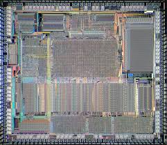
The device is manufactured using Atmel’s high-density nonvolatile memory technology. The On-chip ISP Flash allows the program memory to be reprogrammed in-system through an SPI serial interface, by a conventional nonvolatile memory programmer, or by an On-chip Boot program running on the AVR core.
The boot program can use any interface to download the application program in the application Flash memory. Software in the Boot Flash section will continue to run while the Application Flash section is updated, providing true Read-While-Write operation if Break microcontroller pic16c65b eeprom.
By combining an 8-bit RISC CPU with In-System Self-Program mable Flash on a monolithic ch ip, the Atmel ATmega2561 is a powerful microcontroller that provides a highly flexible and cost effective solution to many embedded control applications.
The ATmega2561 AVR is supported with a full suite of program and system development tools including: C compilers, macro assemblers, program debugger/simulators, in-circuit emulators, and evaluation kits after recover mcu pic16f687 software.
Each device in the ATmeg2561 family differs only in memory size and number of pins. Table 1 summarizes the different configurations for the six devices.
Port A is an 8-bit bi-directional I/O port with internal pull-up resistors (selected for each bit). The Port A output buffers have symmetrical drive characteristics with both high sink and source capability. As inputs, Port A pins that are externally pulled low will source current if the pull-up resistors are activated when copy microcontroller pic16f677 code.
The Port A pins are tri-stated when a reset condition becomes active, even if the clock is not running. Port B is an 8-bit bi-directional I/O port with internal pull-up resistors (selected for each bit). The Port B output buffers have symmetrical drive characteristics with both high sink and source capability. As inputs, Port B pins that are externally pulled low will source current if the pull-up resistors are activated.
The Port B pins are tri-stated when a reset condition becomes active, even if the clock is not running. Port C is an 8-bit bi-directional I/O port with internal pull-up resistors (selected for each bit). The Port C output buffers have symmetrical drive characteristics with both high sink and source capability.
As inputs, Port C pins that are externally pulled low will source current if the pull-up resistors are activated. The Port C pins are tri-stated when a reset condition becomes active, even if the clock is not running.
Break IC PIC16C556A Software
Break IC PIC16C556A and make mcu pic16c556a clone which is provide the same functions as original one after read microcontroller Software from embedded memory;
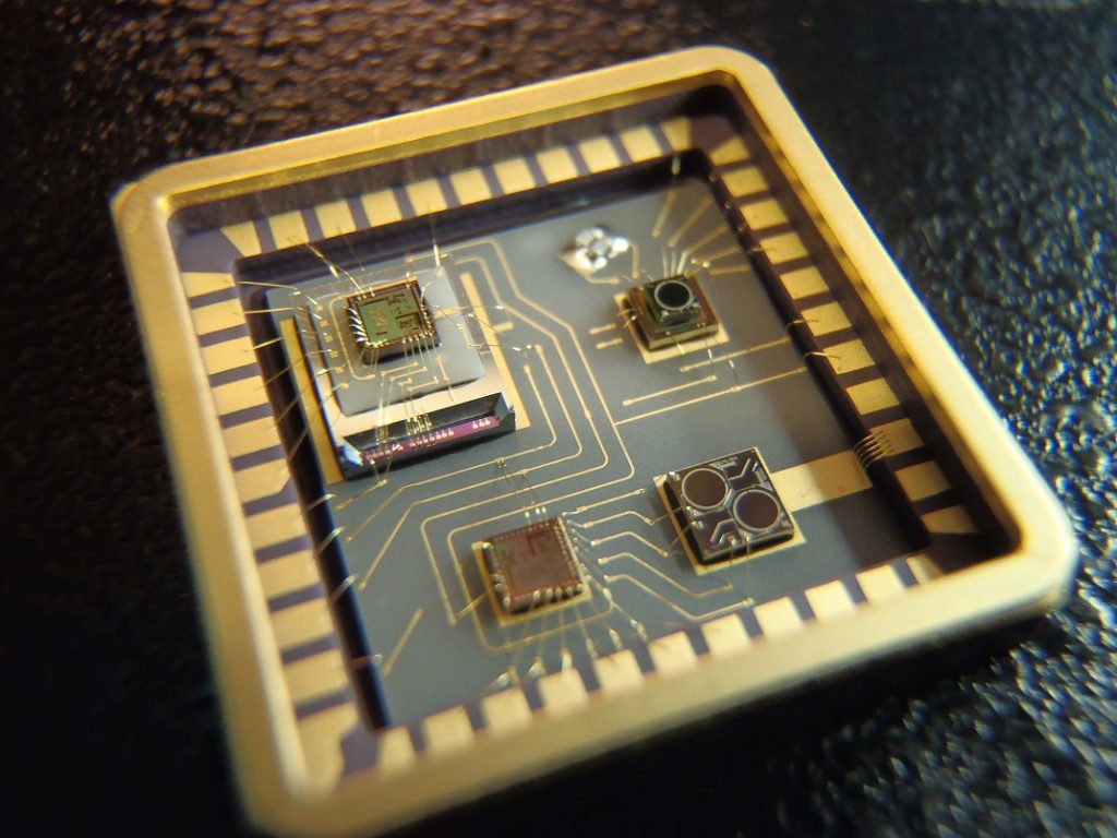
Table 1-1 shows the features of the PIC16C55X(A) mid-range microcontroller families. A simplified block diagram of the PIC16C55X(A) is shown in Figure 3-1.
The PIC16C55X(A) series fit perfectly in applications ranging from motor control to low-power remote sensors. The EPROM technology makes customization of application programs (detection levels, pulse generation, timers, etc.) extremely fast and convenient. The small footprint packages make this microcontroller series perfect for all applications with space limitations.
Low-cost, low-power, high-performance, ease of use and I/O flexibility make the PIC16C55X(A) very versatile.
Those users familiar with the PIC16C5X family of microcontrollers will realize that this is an enhanced version of the PIC16C5X architecture. Please refer to Appendix A for a detailed list of enhancements. Code written for PIC16C5X can be easily ported to PIC16C55X(A) family of devices (Appendix B).
The PIC16C55X(A) family fills the niche for users wanting to migrate up from the PIC16C5X family and not needing various peripheral features of other members of the PIC16XX mid-range microcontroller family.
The PIC16C55X(A) family is supported by a full-featured macro assembler, a software simulator, an in-circuit emulator, a low-cost development programmer and a full-featured programmer. A “C” compiler and fuzzy logic support tools are also available.
A variety of frequency ranges and packaging options are available. Depending on application and production requirements the proper device option can be selected using the information in the PIC16C55X(A) Product Identification System section at the end of this data sheet. When placing orders, please use this page of the data sheet to specify the correct part number.
Break IC SN8P2606 Binary
We can Break IC SN8P2606 Binary, please view the IC SN8P2606 features for your reference:
The power on reset depend no LVD operation for most power-up situations. The power supplying to system is a rising curve and needs some time to achieve the normal voltage. Power on reset sequence is as following:
Power-up: System detects the power voltage up and waits for power stable.
External reset (only external reset pin enable): System checks external reset pin status. If external reset pin is not high level, the system keeps reset status and waits external reset pin released if Break IC SN8P2606 Binary.
System initialization: All system registers is set as initial conditions and system is ready.
Oscillator warm up: Oscillator operation is successfully and supply to system clock.
Program executing: Power on sequence is finished and program executes from ORG 0.
Watchdog reset is a system protection. In normal condition, system works well and clears watchdog timer by program.
Under error condition, system is in unknown situation and watchdog can’t be clear by program before watchdog timer overflow. Watchdog timer overflow occurs and the system is reset. After watchdog reset, the system restarts and returns normal mode. Watchdog reset sequence is as following.
Watchdog timer status: System checks watchdog timer overflow status. If watchdog timer overflow occurs, the system is reset before Break IC SN8P2606 Binary.
System initialization: All system registers is set as initial conditions and system is ready.
Oscillator warm up: Oscillator operation is successfully and supply to system clock.
Program executing: Power on sequence is finished and program executes from ORG 0 when Break IC SN8P2606 Binary.
Watchdog reset is a system protection. In normal condition, system works well and clears watchdog timer by program.
Under error condition, system is in unknown situation and watchdog can’t be clear by program before watchdog timer overflow. Watchdog timer overflow occurs and the system is reset. After watchdog reset, the system restarts and returns normal mode. Watchdog reset sequence is as following.
Watchdog timer status: System checks watchdog timer overflow status. If watchdog timer overflow occurs, the system is reset.
System initialization: All system registers is set as initial conditions and system is ready.
Oscillator warm up: Oscillator operation is successfully and supply to system clock.
Program executing: Power on sequence is finished and program executes from ORG 0. Watchdog timer application note is as following after Break IC SN8P2606 Binary.
Before clearing watchdog timer, check I/O status and check RAM contents can improve system error. Don’t clear watchdog timer in interrupt vector and interrupt service routine. That can improve main routine fail. Clearing watchdog timer program is only at one part of the program. This way is the best structure to enhance the watchdog timer function.
Break Chip PIC12CE518 Binary
Break Chip PIC12CE518 Flash memory and read pic12ce518 mcu binary from embedded memory after copy the embedded code to new microcontroller;
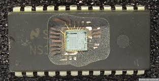
As a program instruction is executed, the Program Counter (PC) will contain the address of the next program instruction to be executed. The PC value is increased by one every instruction cycle, unless an instruction changes the PC.
For a GOTO instruction, bits 8:0 of the PC are provided by the GOTO instruction word. The PC Latch (PCL) is mapped to PC<7:0>. Bit 5 of the STATUS register provides page information to bit 9 of the PC (Figure 4- 8) if extract pic16f84 mcu firmware.
For a CALL instruction, or any instruction where the PCL is the destination, bits 7:0 of the PC again are provided by the instruction word. However, PC<8> does not come from the instruction word, but is always cleared.
Instructions where the PCL is the destination, or Modify PCL instructions, include MOVWF PC, ADDWF PC, and BSF PC,5.
The Program Counter is set upon a RESET, which means that the PC addresses the last location in the last page i.e., the oscillator calibration instruction. After executing MOVLW XX, the PC will roll over to location 00h, and begin executing user code.
The STATUS register page preselect bits are cleared upon a RESET, which means that page 0 is pre-selected.
Therefore, upon a RESET, a GOTO instruction will automatically cause the program to jump to page 0 until the value of the page bits is altered. PIC12C5XX devices have a 12-bit wide L.I.F.O. hardware push/pop stack.
A CALL instruction will push the current value of stack 1 into stack 2 and then push the current program counter value, incremented by one, into stack level 1. If more than two sequential CALL’s are executed, only the most recent two return addresses are stored when crack mc68hc05b6 Chip.
ARETLW instruction will pop the contents of stack level 1 into the program counter and then copy stack level contents into level 1. If more than two sequential RETLW’s are executed, the stack will be filled with the address previously stored in level 2. Note that the W register will be loaded with the literal value specified in the instruction. This is particularly useful for the implementation of data look-up tables within the program memory.
Upon any reset, the contents of the stack remain unchanged, however the program counter (PCL) will also be reset to Break MCU Chip.
Break IC ATmega1280 Eeprom
Break IC ATmega1280 Eeprom and read the firmware from mcu atmega1280 memory, and crack microcontroller atmega1280 security fuse bit by focus ion beam technology;
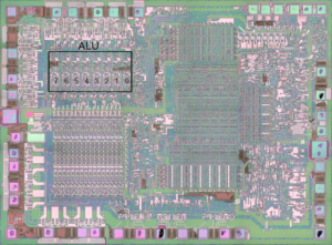
Port A is an 8-bit bi-directional I/O port with internal pull-up resistors (selected for each bit). The Port A output buffers have symmetrical drive characteristics with both high sink and source capability. As inputs, Port A pins that are externally pulled low will source current if the pull-up resistors are activated.
The Port A pins are tri-stated when a reset condition becomes active, even if the clock is not running. Port B is an 8-bit bi-directional I/O port with internal pull-up resistors (selected for each bit). The Port B output buffers have symmetrical drive characteristics with both high sink and source capability if recover mcu pic18f452 program.
As inputs, Port B pins that are externally pulled low will source current if the pull-up resistors are activated. The Port B pins are tri-stated when a reset condition becomes active, even if the clock is not running.
Port C is an 8-bit bi-directional I/O port with internal pull-up resistors (selected for each bit). The Port C output buffers have symmetrical drive characteristics with both high sink and source capability. As inputs, Port C pins that are externally pulled low will source current if the pull-up resistors are activated. The Port C pins are tri-stated when a reset condition becomes active, even if the clock is not running.
Port D is an 8-bit bi-directional I/O port with internal pull-up resistors (selected for each bit). The Port D output buffers have symmetrical drive characteristics with both high sink and source capability. As inputs, Port D pins that are externally pulled low will source current if the pull-up resistors are activated.
The Port D pins are tri-stated when a reset condition becomes active, even if the clock is not running. Port E is an 8-bit bi-directional I/O port with internal pull-up resistors (selected for each bit). The Port E output buffers have symmetrical drive characteristics with both high sink and source capability.
As inputs, Port E pins that are externally pulled low will source current if the pull-up resistors are activated. The Port E pins are tri-stated when a reset condition becomes active, even if the clock is not running.
Port F serves as analog inputs to the A/D Converter. Port F also serves as an 8-bit bi-directional I/O port, if the A/D Converter is not used. Port pins can provide internal pull-up resistors (selected for each bit). The Port F output buffers have symmetrical drive characteristics with both high sink and source capability after Break IC.
As inputs, Port F pins that are externally pulled low will source current if the pull-up resistors are activated. The Port F pins are tri-stated when a reset condition becomes active, even if the clock is not running. If the JTAG interface is enabled, the pull-up resistors on pins PF7(TDI), PF5(TMS), and PF4(TCK) will be activated even if a reset occurs.
Port G is a 6-bit I/O port with internal pull-up resistors (selected for each bit). The Port G output buffers have symmetrical drive characteristics with both high sink and source capability. As inputs, Port G pins that are externally pulled low will source current if the pull-up resistors are activated. The Port G pins are tri-stated when a reset condition becomes active, even if the clock is not running.
Port H is a 8-bit bi-directional I/O port with internal pull-up resistors (selected for each bit). The Port H output buffers have symmetrical drive characteristics with both high sink and source capability. As inputs, Port H pins that are externally pulled low will source current if the pull-up resistors are activated. The Port H pins are tri-stated when a reset condition becomes active, even if the clock is not running.
Break IC ATmega640V Flash
Break IC ATmega640V and readout the embedded firmware from mcu atmega640v Flash memory and eeprom memory, the protective system of microcontroller atmega640v will be cracked to get access to flash and eeprom memory;
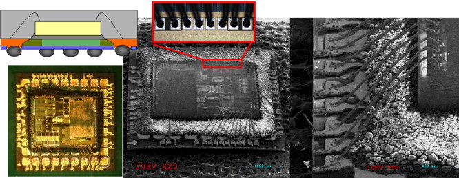
The ATmega640V is a low-power CMOS 8-bit microcontroller based on the AVR enhanced RISC architecture. By executing powerful instructions in a single clock cycle, the ATmega640V achieves throughputs approaching 1 MIPS per MHz allowing the system designer to optimize power consumption versus processing speed.
The AVR core combines a rich instruction set with 32 general purpose working registers. All the 32 registers are directly connected to the Arithmetic Logic Unit (ALU), allowing two independent registers to be accessed in one single instruction executed in one clock cycle.
T5he resulting architecture is more code efficient while achieving throughputs up to ten times faster than conventional CISC microcontrollers before attack microcontroller mc68hc705p6.
The ATmega640V provides the following features: 64K/128K/256K bytes of In-System Programmable Flash with Break-While-Write capabilities, 4K bytes EEPROM, 8K bytes SRAM, 54/86 general purpose I/O lines, 32 general purpose working registers, Real Time Counter (RTC), six flexible Timer/Counters with compare modes and PWM, 4 USARTs, a byte oriented 2-wire Serial Interface, a 16-channel, 10-bit ADC with optional differential input stage with programmable gain, programmable Watchdog Timer with Internal Oscillator, an SPI serial port, IEEE std. 1149.1 compliant JTAG test interface, also used for accessing the On-IC Debug system and programming and six software selectable power saving modes.
The Idle mode stops the CPU while allowing the SRAM, Timer/Counters, SPI port, and interrupt system to continue functioning. The Power-down mode saves the register contents but freezes the Oscillator, disabling all other IC functions until the next interrupt or Hardware Reset when copy pic16lf877 mcu program.
In Power save mode, the asynchronous timer continues to run, allowing the user to maintain a timer base while the rest of the device is sleeping. The ADC Noise Reduction mode stops the CPU and all I/O modules except Asynchronous Timer and ADC, to minimize switching noise during ADC conversions.
In Standby mode, the Crystal/Resonator Oscillator is running while the rest of the device is sleeping. This allows very fast start-up combined with low power consumption. In Extended Standby mode, both the main Oscillator and the Asynchronous Timer continue to run.
The device is manufactured using Atmel’s high-density nonvolatile memory technology. The On-IC ISP Flash allows the program memory to be reprogrammed in-system through an SPI serial interface, by a conventional nonvolatile memory programmer, or by an On-IC Boot program running on the AVR core when Break IC.
The boot program can use any interface to download the application program in the application Flash memory. Software in the Boot Flash section will continue to run while the Application Flash section is updated, providing true Break-While-Write operation.
By combining an 8-bit RISC CPU with In-System Self-Programmable Flash on a monolithic IC, the Atmel ATmega640V is a powerful microcontroller that provides a highly flexible and cost effective solution to many embedded control applications.
The ATmega640V AVR is supported with a full suite of program and system development tools including: C compilers, macro assemblers, program debugger/simulators, in-circuit emulators, and evaluation kits.
Break IC ATtiny261 Code
Break IC ATtiny261 secured memory and extract mcu attiny261 Code from flash and eeprom memory, include program and data in the format of heximal, in the software extraction process from Microcontroller attiny261, the security fuse bit will be cracked;
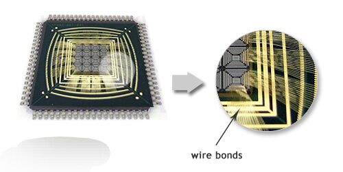
High Performance, Low Power AVR® 8-Bit Microcontroller
Advanced RISC Architecture
– 123 Powerful Instructions – Most Single Clock Cycle Execution
– 32 x 8 General Purpose Working Registers
– Fully Static Operation
Non-volatile Program and Data Memories
– 2/4/8K Byte of In-System Programmable Program Memory Flash
(ATtiny261/461/861)
Endurance: 10,000 Write/Erase Cycles if recovr stm32f107rct6 IC
– 128/256/512 Bytes In-System Programmable EEPROM (ATtiny261/461/861)
Endurance: 100,000 Write/Erase Cycles
– 128/256/512 Bytes Internal SRAM (ATtiny261/461/861)
– Programming Lock for Self-Programming Flash Program and EEPROM Data Security
Peripheral Features
– 8/16-bit Timer/Counter with Prescaler and Two PWM Channels
– 8/10-bit High Speed Timer/Counter with Separate Prescaler
3 High Frequency PWM Outputs with Separate Output Compare Registers
Programmable Dead Time Generator
– Universal Serial Interface with Start Condition Detector when copy at89s8252 flash memory content
– 10-bit ADC
11 Single Ended Channels
16 Differential ADC Channel Pairs
15 Differential ADC Channel Pairs with Programmable Gain (1x, 8x, 20x, 32x)
– Programmable Watchdog Timer with Separate On-chip Oscillator
– On-chip Analog Comparator
Special Microcontroller Features
– debugWIRE On-chip Debug System
– In-System Programmable via SPI Port
– External and Internal Interrupt Sources
– Low Power Idle, ADC Noise Reduction, and Power-down Modes
– Enhanced Power-on Reset Circuit
– Programmable Brown-out Detection Circuit
– Internal Calibrated Oscillator
I/O and Packages
– 16 Programmable I/O Lines
– 20-pin PDIP, 20-pin SOIC and 32-pad MLF
Operating Voltage:
– 1.8 – 5.5V for ATtiny261V/461V/861V
– 2.7 – 5.5V for ATtiny261/461/861
Speed Grade:
– ATtiny261V/461V/861V: 0 – 4 MHz @ 1.8 – 5.5V, 0 – 10 MHz @ 2.7 – 5.5V
– ATtiny261/461/861: 0 – 10 MHz @ 2.7 – 5.5V, 0 – 20 MHz @ 4.5 – 5.5V
– Active Mode: 1 MHz, 1.8V: 380ìA
– Power-down Mode: 0.1ìA at 1.8V
Typical values contained in this data sheet are based on simulations and characterization of other AVR microcontrollers manufactured on the same process technology. Min and Max values will be available after the device is characterized before Break IC.
The ATtiny261/461/861 is a low-power CMOS 8-bit microcontroller based on the AVR enhanced RISC architecture. By executing powerful instructions in a single clock cycle, the ATtiny261/461/861 achieves throughputs approaching 1 MIPS per MHz allowing the system designer to optimize power consumption versus processing speed after Break IC.
 Posted in Break IC |
  Tags: break ic source data, break ic source eeprom, break ic source file, break ic source firmware, break ic source heximal, break ic source information, break ic source memory, break ic source program |
  Comments Closed
Break IC ATtiny2313 Code
Break IC ATtiny2313 tamper resistance system, extract Code from chip attiny2313 memory after avr microcontroller attiny2313 flash memory has been broken;
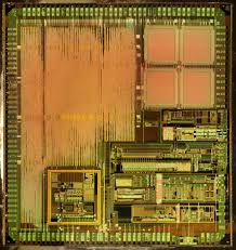
High Performance, Low Power AVR® 8-Bit Microcontroller
Advanced RISC Architecture
– 120 Powerful Instructions – Most Single Clock Cycle Execution
– 32 x 8 General Purpose Working Registers
– Fully Static Operation
– Up to 20 MIPS Throughput at 20 MHz
Data and Non-volatile Program and Data Memories
– 2/4K Bytes of In-System Self Programmable Flash
Endurance 10,000 Write/Erase Cycles
– 128/256 Bytes In-System Programmable EEPROM
Endurance: 100,000 Write/Erase Cycles
– 128/256 Bytes Internal SRAM when Break IC
– Programming Lock for Flash Program and EEPROM Data Security
Peripheral Features
– One 8-bit Timer/Counter with Separate Prescaler and Compare Mode
– One 16-bit Timer/Counter with Separate Prescaler, Compare and Capture Modes
– Four PWM Channels
– On-chip Analog Comparator
– Programmable Watchdog Timer with On-chip Oscillator
– USI – Universal Serial Interface
– Full Duplex USART
Special Microcontroller Features
– debugWIRE On-chip Debugging
– In-System Programmable via SPI Port
– External and Internal Interrupt Sources
– Low-power Idle, Power-down, and Standby Modes
– Enhanced Power-on Reset Circuit if Break mcu atmega16pa flash
– Programmable Brown-out Detection Circuit
– Internal Calibrated Oscillator
I/O and Packages
– 18 Programmable I/O Lines
– 20-pin PDIP, 20-pin SOIC, 20-pad MLF/VQFN
Operating Voltage
– 1.8 – 5.5V
Speed Grades
– 0 – 4 MHz @ 1.8 – 5.5V
– 0 – 10 MHz @ 2.7 – 5.5V
– 0 – 20 MHz @ 4.5 – 5.5V
Industrial Temperature Range: -40°C to +85°C
Low Power Consumption
In-System
Programmable Flash
– Active Mode
190 µA at 1.8V and 1MHz
– Idle Mode
24 µA at 1.8V and 1MHz
– Power-down Mode
0.1 µA at 1.8V and +25°C
Port A is a 3-bit bi-directional I/O port with internal pull-up resistors (selected for each bit). The Port A output buffers have symmetrical drive characteristics with both high sink and source capability, except PA2 which has the RESET capability.
To use pin PA2 as I/O pin, instead of RESET pin, program (“0”) RSTDISBL fuse. As inputs, Port A pins that are externally pulled low will source current if the pull-up resistors are activated. The Port A pins are tri-stated when a reset condition becomes active, even if the clock is not running after Break IC.
Posted in Break IC |
Tags: break ic source data, break ic source eeprom, break ic source file, break ic source firmware, break ic source heximal, break ic source information, break ic source memory, break ic source program |
Comments Closed
Break IC ATtiny85V Software
Break IC ATtiny85V can help engineer to readout the embedded firmware from mcu attiny85v flash and eeprom memory, fuse bit of microcontroller attiny85v can be cracked;
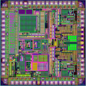
Break IC ATtiny85V can help engineer to readout the embedded firmware from mcu attiny85v flash and eeprom memory, fuse bit of microcontroller attiny85v can be cracked
XTAL1 and XTAL2 are the input and output, respectively, of an inverting amplifier which can be configured for use as an on-IC oscillator, as shown in Figure 1. Either a quartz crystal or ceramic resonator may be used. To drive the device from an external clock source, XTAL2 should be left unconnected while XTAL1 is driven as shown in Figure 2. There are no requirements on the duty cycle of the external clock signal, since the input to the internal clocking circuitry is through a divide-by-two flip-flop, but minimum and maximum voltage high and low time specifications must be observed.
In idle mode, the CPU puts itself to sleep while all the on-IC peripherals remain active. The mode is invoked by software. The content of the on-IC RAM and all the special functions registers remain unchanged during Break mcu pic16f876 memory.
Figure 2. External Clock Drive Configuration mode. The idle mode can be terminated by any enabled interrupt or by a hardware reset before Break IC. It should be noted that when idle is terminated by a hardware reset, the device normally resumes program execution, from where it left off, up to two machine cycles before the internal reset algorithm takes control. On-IC hardware inhibits access to internal RAM in this event, but access to the port pins is not inhibited.
To eliminate the possibility of an unexpected write to a port pin when Idle is terminated by reset, the instruction following the one that invokes Idle should not be one that writes to a port pin or to external memory. In the power down mode the oscillator is stopped, and the instruction that invokes power down is the last instruction executed. The on-IC RAM and Special Function Registers retain their values until the power down mode is terminated.
The only exit from power down is a hardware reset. Reset redefines the SFRs but does not change the on-IC RAM. The reset should not be activated before VCC is restored to its normal operating level and must be held active long enough to allow the oscillator to restart and stabilize if Break IC.
Posted in Break IC |
Tags: break ic source data, break ic source eeprom, break ic source file, break ic source firmware, break ic source hex, break ic source information, break ic source memory, break ic source program |
Comments Closed
Break PLD PALCE16V8H-15JC Software
The PALCE16V8H-15JC is a classic programmable logic device (PLD) widely adopted in legacy digital systems where fast combinational logic, deterministic timing, and compact design are required. It has been extensively used in industrial controllers, telecommunications interfaces, instrumentation equipment, automotive subsystems, and embedded control boards. Unlike microcontrollers that rely on sequential firmware execution, this PLD implements hardware-defined logic through programmed fuse maps, allowing stable and predictable operation. However, when the original design archive, logic file, or source code is missing, maintaining or reproducing such systems becomes extremely challenging. The Break PLD PALCE16V8H-15JC Software service is designed to help authorized users recover and reconstruct this critical embedded logic data from secured devices.
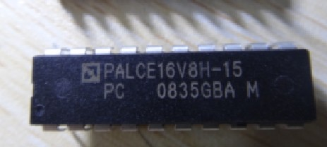
In many deployed systems, the PALCE16V8H-15JC is configured with protective, protected, locked, or secured fuse settings that prevent access to its internal memory and configuration data. These mechanisms ensure that the PLD’s programmed logic—stored in binary or heximal fuse maps—cannot be directly read out. Our service focuses on helping clients attack, break, or carefully decode these restrictions through advanced engineering analysis. By studying the embedded structure of the PLD, we can retrieve logic configuration data, reconstruct the internal program, and rebuild a usable archive even when the device is fully protected. In complex cases, controlled decapsulate approaches may be applied to access deeply embedded fuse structures, enabling extraction of configuration patterns from otherwise inaccessible regions. The process ensures that recovered binary or heximal data accurately reflects the original programmed logic without compromising reliability.
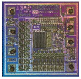
We can Break PLD PALCE16V8H-15JC Software, please view below PLD PALCE16V8H-15JC features for your reference:
DISTINCTIVE CHARACTERISTICS
Pin and function compatible with all 20-pin GAL devices
Electrically erasable CMOS technology provides reconfigurable logic and full testability
High-speed CMOS technology
— 5-ns propagation delay for “-5” version
— 7.5-ns propagation delay for “-7” version
Direct plug-in replacement for the PAL16R8 series and most of the PAL10H8 series
Outputs programmable as registered or combinatorial in any combination, Peripheral Component Interconnect (PCI) compliant.
GENERAL DESCRIPTION
The PALCE16V8 is an advanced PAL device built with low-power, high-speed, electrically-erasable CMOS technology. It is functionally compatible with all 20-pin GAL devices. The macrocells provide a universal device architecture. The PALCE16V8 will directly replace the PAL16R8 and PAL10H8 series devices, with the exception of the PAL16C1.
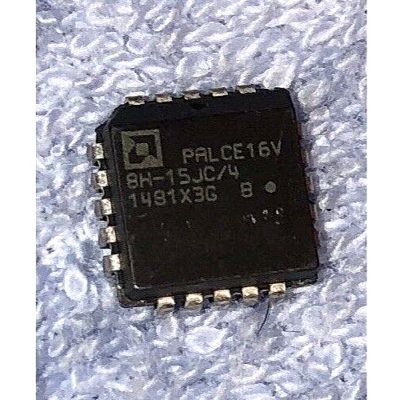
The PALCE16V8 utilizes the familiar sum-of-products (AND/OR) architecture that allows users to implement complex logic functions easily and efficiently. Multiple levels of combinatorial logic can always be reduced to sum-of-products form, taking advantage of the very wide input gates available in PAL devices. The equations are programmed into the device through floating gate cells in the AND logic array that can be erased electrically.
Programmable output polarity
Programmable enable/disable control
Preloadable output registers for testability
Automatic register reset on power up
Cost-effective 20-pin plastic DIP, PLCC, and SOIC packages
Extensive third-party software and programmer support through FusionPLD partners
Fully tested for 100% programming and functional yields and high reliability
5 ns version utilizes a split leadframe for improved performance.
The fixed OR array allows up to eight data product terms per output for logic functions. The sum of these products feeds the output macrocell. Each macrocell can be programmed as registered or combinatorial with an active high or active-low output. The output configuration is determined by two global bits and one local bit controlling four multiplexers in each macrocell. AMD’s FusionPLD program allows PALCE16V8 designs to be implemented using a wide variety of popular industry-standard design tools. By working closely with the FusionPLD partners, AMD certifies that the tools provide accurate, quality support. By ensuring that third party tools are available, costs are lowered because a designer does not have to buy a complete set of new tools for each device. The Fusion PLD program also greatly reduces design time since a designer can use a tool that is already installed and familiar.
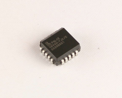
Once the configuration data is successfully retrieved, it must be translated into a meaningful representation for engineering use. The extracted binary fuse map is decoded into logical equations or equivalent structures, allowing partial or full reconstruction of the original source code or design intent. This enables clients to clone or duplicate the PLD functionality on compatible devices or migrate the design into modern programmable platforms such as CPLDs or FPGAs. Even though the PALCE16V8H-15JC does not store traditional firmware, its programmed logic serves as a functional equivalent of an embedded program, and recovering this information is essential for system continuity.
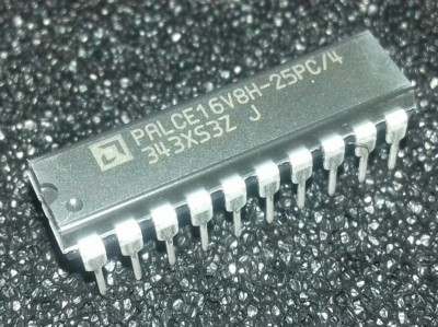
For manufacturers, system integrators, and maintenance providers, the Break PLD PALCE16V8H-15JC Software service offers significant practical benefits. It allows legacy equipment to remain operational, avoids costly redesign efforts, and preserves valuable embedded logic that may no longer be documented. Instead of replacing entire systems due to locked or encrypted PLD devices, organizations can regain access to their configuration data, logic program, and design archive. By combining deep expertise in programmable logic devices with careful handling of protected and secured environments, this service provides a reliable pathway to recover, reuse, and extend critical embedded system functionality across a wide range of industries.