Archive for the ‘Break IC’ Category
 Break ATmel Locked Chip ATmega1281V Program
 January 11th, 2012 |
  Author:
 We can break ATmel locked chip ATMEGA1281V program, please view the ATmel locked chip ATMEGA1281V features for your reference:
The device is manufactured using Atmel’s high density non-volatile memory technology. The On-chip ISP Flash allows the program memory to be reprogrammed In-System through an SPI serial interface, by a conventional non-volatile memory programmer.
Or by an On-chip Boot program running on the AVR core. The Boot program can use any interface to download the application program in the Application Flash memory.
Software in the Boot Flash section will continue to run while the Application Flash section is updated, providing true Read-While-Write operation before Break ATmel Locked Chip ATmega1281V Program.
By combining an 8-bit RISC CPU with In-System Self-Programmable Flash on a monolithic chip, the Atmel ATMEGA1281V is a powerful microcontroller that provides a highly flexible and cost effective solution to many embedded control applications.
The ATMEGA1281V AVR is supported with a full suite of program and system development tools including: C Compilers, Macro Assemblers, Program Debugger/Simulators, In-Circuit Emulators, and Evaluation kits when Break ATmel Locked Chip ATmega1281V Program.
The ATMEGA1281V differ only in memory sizes, boot loader support, and interrupt vector sizes. Table 2-1 summarizes the different memory and interrupt vector sizes for the devices.
ATMEGA1281V support a real Read-While-Write Self-Programming mechanism. There is a separate Boot Loader Section, and the SPM instruction can only execute from there.
In ATMEGA1281V there is no Read-While-Write support and no separate Boot Loader Section. The SPM instruction can execute from the entire Flash after Break ATmel Locked Chip ATmega1281V Program.
Reliability Qualification results show that the projected data retention failure rate is much less than 1 PPM over 20 years at 85°C or 100 years at 25°C if BREAK IC.
Decrypt Encrypted Microcontroller ATmega16PA Code
We can Decrypt Encrypted Microcontroller ATmega16PA Code, please view the Encrypted Microcontroller ATmega16PA features for your reference:
Port B is a 6-bit I/O port. PB4..0 are I/O pins that can provide internal pull-ups (selected for each bit). PB5 is input or open-drain output.
The use of pin PB5 is defined by a fuse and the special function associated with this pin is external Reset. The port pins are tristated when a reset condition becomes active, even if the clock is not running if decrypt encrypted microcontroller.
The internal oscillator provides a clock rate of nominally 1.6 MHz for the system clock (CK). Due to large initial variation (0.8 -1.6 MHz) of the internal oscillator, a tuning capability is built in.
Through an 8-bit control register – OSCCAL – the system clock rate can be tuned with less than 1% steps of the nominal clock after decrypt encrypted microcontroller.
There is an internal PLL that provides a 16x clock rate locked to the system clock (CK) for the use of the Peripheral Timer/Counter1. The nominal frequency of this peripheral clock, PCK, is 25.6 MHz.
The fast-access register file concept contains 32 x 8-bit general purpose working registers with a single-clock-cycle access time. This means that during one single clock cycle, one ALU (Arithmetic Logic Unit) operation is executed if decrypt encrypted microcontroller.
Two operands are output from the register file, the operation is executed, and the result is stored back in the register file – in one clock cycle.
Two of the 32 registers can be used as a 16-bit pointer for indirect memory access. This pointer is called the Z-pointer, and can address the register file, IO file and the code program memory before decrypt encrypted microcontroller.
The ALU supports arithmetic and logic functions between registers or between a constant and a register. Single-register operations are also executed in the ALU.
Figure 2 shows the ATtiny15L AVR RISC microcontroller architecture. The AVR uses a Harvard architecture concept with separate memories and buses for program and data memories.
The program memory is accessed with a two-stage pipeline. While one instruction is being executed, the next instruction is pre-fetched from the program memory.
This concept enables instructions to be executed in every clock cycle. The program memory is In-System Programmable code memory if Reverse Engineering Microcontroller.
Break Protected Microcontroller ATmega164 Locked Flash
We can break Protected Microcontroller ATMEGA164 locked flash, please view Protected Microcontroller ATMEGA164 features for your reference:
The BOD circuit will only detect a drop in VCC if the voltage stays below the trigger level for longer than 3 µs for trigger level 4.0V, 7 µs for trigger level 2.7V (typical values).
When the Watchdog times out, it will generate a short reset pulse of 1 CK cycle duration. On the falling edge of this pulse, the delay timer starts counting the time-out period tTOUT. Refer to page 34 for details on operation of the Watchdog Timer if Break Protected Microcontroller ATmega164 Locked Flash.
To make use of the reset flags to identify a reset condition, the user should read and then reset the MCUSR as early as possible in the program.
If the register is cleared before another reset occurs, the source of the reset can be found by examining the reset flags. ATmega164 features an internal bandgap reference with a nominal voltage of 1.22V after Break Protected Microcontroller ATmega164 Locked Flash.
This reference is used for Brown-out Detection, and it can be used as an input to the Analog Comparator. The 2.56V reference to the ADC is generated from the internal bandgap reference.
The voltage reference has a start-up time that may influence the way it should be used. The maximum start-up time is TBD. To save power, the reference is not always turned on. The reference is on during the following situations:
1. When the BOD is enabled (by programming the BODEN fuse).
2. When the bandgap reference is connected to the Analog Comparator (by setting the AINBG bit in ACSR).
3. When the ADC is enabled before BREAK IC.
CPLD Crack Method Description
CPLD Crack Method Description refers to describe the way to crack CPLD chip protection system and readout firmware from memory cells;
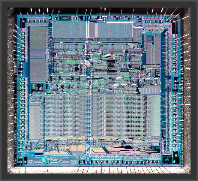
The principle of this technology is exposure internal wire connection, through inspection, manipulation and interfere MCU to achieve CPLD chip program information purpose.
For more convenience, people can separate above 4 methods into 2 categories: 1 is intruded cpld attacking encrypted code, this kind of crack will need to decap the package, and then by the assistance of semiconductor testing device, microscope and mini-locator, spend several hours or even weeks can finish in a dedicated lab.
All the probe technology can be classified as intruded cpld crack. The other 3 ways belong to un-intruded crack, objects wouldn’t be damaged physically. In some occasion un-intruded CPLD ic source code attacking is very dangerous, that is because un-intruded device can be self-made and upgrade, cost is very low.
A majority of un-intrude cpld need hacker have good knowledge of microprocessor and software. On the contrary, intruded probe cpld mcu ic hack don’t need too much knowledge, moreover can use a set of similar technology to deal with products in wider scope. As a result of that, CPLD hacking normally start from intruded IC crack, accumulated experience will help you develop more economical and faster un-intruded crack technology.
 Posted in Break IC |
  Tags: cpld attack, cpld break, cpld copy, cpld decode, cpld decryption, cpld extract, cpld recover |
  Comments Closed
FPGA Crack method
FPGA crack’s Error-Occurring technology
Through abnormal operation situation to let errors occur in FPGA, and then provide extra accessing to crack FPGA, the most commonly used error-occurring methods include voltage shock and clock shock, low voltage and high voltage fpga crack can be applied for prohibition of circuit protection or force microprocessor to operate errors. Clock transient hop maybe can re-set circuit protection but won’t damage protected information. Power supply and clock transient hop can affect recovery and execution of single order in part of FPGA.
Posted in Break IC |
Tags: fpga attack, fpga break, fpga copy, fpga decrypt, fpga extract, fpga recover |
Comments Closed
How to Extract MCU Code
How to Extract MCU Code is a task for engineers who wants to make IC clone from exisiting microcontroller memory reading;
The principle of this method is monitor simulation characteristic of all the power supply and interface connection during the standard operation under high resolution, and copy MCU firmware by monitoring its electromagnetic radiation.
Because MCU is an active electronic component, when it operate different orders, corresponding power supply consumption will alter accordingly. Then use special electronic measurement device and mathematic statistical method to analyze and detect these changes, can extract code embedded inside microprocessor.
Currently RF programmer can read program of old MCU is base upon this principle.
Attack MCU Method Introduction
Attack MCU Method can be categorized with invasive and semi-invasive ones, through which will be able to extract code from IC chip and make microcontroller clone;
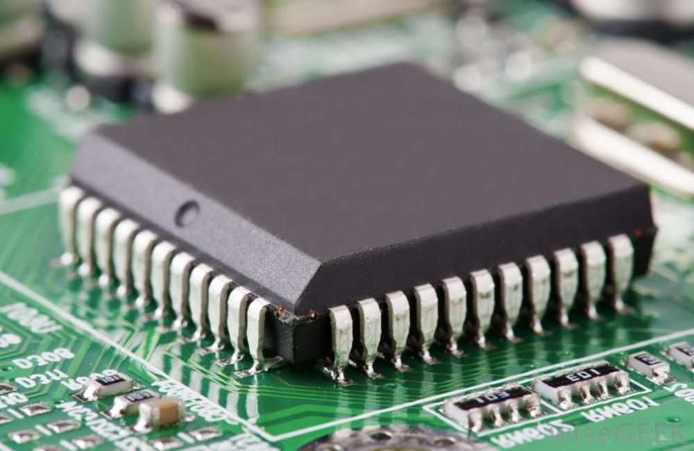
1 — Software MCU Attack:
This method use communication interface of processor plus protocol, encrypted algorithm to attack microcontroller, a typical successful example of software attack is the breaking against early MCU ATMEL AT89C51 series MCU. Attacker takes advantage of the design flaw of erasure operation sequence, use self-made program to erase encrypted lock location, and then halt the next operation of erase internal program, through which the encrypted MCU being turn into decrypted MCU after attacked, finally use programmer to read the internal procedure.
Currently base upon the other encryption method, some kind of devices can be promoted accompany with certain types of software can be used as software mcu attack. In recent days, domestic market has presented a kind of 51 MCU cracking device, this decipher is mainly focus on brands like SyncMos, Winbond, use the leak of the production technology and insert positioning bit of several programmer, find out continuous empty locations through certain methods, which means need to find out the continuous FF FF bits, those inserted bits can instruct the order of send internal program to outside environment, and then use processor attack device to intercept and capture.
Posted in Break IC |
Tags: cpld mcu attack, dsp mcu attack, mcu attack, mcu ic attack |
Comments Closed
MCU Break Introduction
MCU Break is a process to disable the secured protection against unauthorized MCU reading, focus ion beam technique will be applied to remove the fuse bit to expose the flash memory;
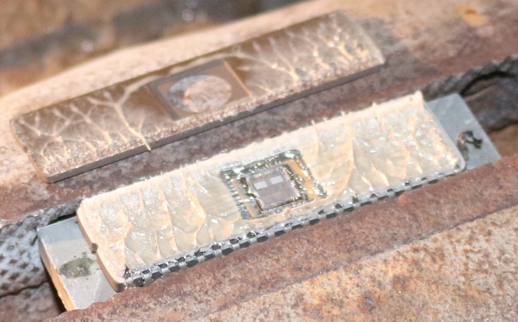
Microcontrollers generally have internal EEPROM / FLASH program for users to store data. To prevent unauthorized access or copy microcontroller program of MCU (MCU crack), most of MCUs are encrypted with the encryption lock orientation or lock-bit bytes to protect the MCU program.
If the programming lock-bit encryption is enabled (locked), you can’t use ordinary programmer reads the program directly within MCU, which is called encryption or MCU locking.
MCU IC breaker with special equipment or home-made equipment, take the advantage of single IC design flaw or software defects, through a variety of techniques, can attack key information from the MCU, access to program inside microcontroller, which is called microcontroller break.
Please view our service procedures below for your reference:
Step 1:
After recipient of original MCU from customer and finish the electrical integrity test to confirm the feasibility of work, official invoice will be sent from us, customer prepay 50% payment, we start the project upon the confirmation of payment recipient;
Step 2:
After process finish and informed by us, program will be loaded into two pieces of new empty MCUs and send back to customer for verification, customer need to pay freight cost and new MCU samples cost in advance;
Step 3:
Customer has obliged to inform the test result within 5 working days after receipt of programmed MCU samples, if test is passed, customer need to pay the balance within 72 hours and we will send the program to customer through email after confirm the receipt of customer balance payment within 48 hours;
Step 4:
If the samples don’t work, it is obliged to take necessary evaluation after the receipt of functionality testing platform for debugging and resubmit samples within 3 weeks, and if still fail to find and solve the problems, we have to refund customer all of prepayment within 2 weeks upon the date of mutual agreement. (Include MCU samples price and freight cost).
If you have any further inquiry regarding our service please feel free to let us know, thanks
Posted in Break IC |
Tags: cpld mcu break, dsp mcu break, mcu break, mcu chip break, mcu ic break |
Comments Closed
Break MCU ATmega128PA Heximal
Break MCU ATmega128APA flash memory and readout chip ATmega128PA content inside it in the format of Heximal, the code can be reprogrammed to new ATmega128PA microcontroller for cloning;
OC1A/PCINT5, Bit 5
OC1A, Output Compare Match A output: The PB5 pin can serve as an external output for the Timer/Counter1 Output Compare A. The pin has to be configured as an output (DDB5 set (one)) to serve this function. The OC1A pin is also the output pin for the PWM mode timer function.
PCINT5, Pin Change Interrupt source 5: The PB7 pin can serve as an external interrupt source.
OC2A/PCINT4, Bit 4
OC2A, Output Compare Match output: The PB4 pin can serve as an external output for the Timer/Counter2 Output Compare. The pin has to be configured as an output (DDB4 set (one)) to serve this function. The OC2A pin is also the output pin for the PWM mode timer function when recover mcu pic16c554 software.
PCINT4, Pin Change Interrupt source 4: The PB7 pin can serve as an external interrupt source.
MISO/PCINT3 – Port B, Bit 3
MISO: Master Data input, Slave Data output pin for SPI channel. When the SPI is enabled as a master, this pin is configured as an input regardless of the setting of DDB3. When the SPI is enabled as a slave, the data direction of this pin is controlled by DDB3. When the pin is forced to be an input, the pull-up can still be controlled by the PORTB3 bit.
PCINT3, Pin Change Interrupt source 3: The PB7 pin can serve as an external interrupt source when Break MCU heximal.
MOSI/PCINT2 – Port B, Bit 2
MOSI: SPI Master Data output, Slave Data input for SPI channel. When the SPI is enabled as a slave, this pin is configured as an input regardless of the setting of DDB2. When the SPI is enabled as a master, the data direction of this pin is controlled by DDB2. When the pin is forced to be an input, the pull-up can still be controlled by the PORTB2 bit.
PCINT2, Pin Change Interrupt source 2: The PB7 pin can serve as an external interrupt source.
SCK/PCINT1 – Port B, Bit 1
SCK: Master Clock output, Slave Clock input pin for SPI channel. When the SPI is enabled as a slave, this pin is configured as an input regardless of the setting of DDB1. When the SPI0 is enabled as a master, the data direction of this pin is controlled by DDB1. When the pin is forced to be an input, the pull-up can still be controlled by the PORTB1 bit.
PCINT1, Pin Change Interrupt source 1: The PB7 pin can serve as an external interrupt source.
Posted in Break IC |
Tags: break mcu encrypted archive, break mcu encrypted binary, break mcu encrypted code, break mcu encrypted content, break mcu encrypted data, break mcu encrypted eeprom, break mcu encrypted file, break mcu encrypted firmware, break mcu encrypted heximal, break mcu encrypted information, break mcu encrypted memory, break mcu encrypted program |
Comments Closed
Break IC PIC18F4620 Program
Break IC PIC18F4620 security fuse bit and read PIC18F4620 program from flash memory, then copy eeprom content from protected microchip PIC18F4620 processor;
Possible Hardware fuse Watchdog always on (WDTON) for fail-safe modeThe Watchdog Timer (WDT) is a timer counting cycles of a separate on-chip 128 kHz oscillator.
The WDT gives an interrupt or a system reset when the counter reaches a given time-out value. In normal operation mode, it is required that the system uses the WDR – Watchdog Timer Reset – instruction to restart the counter before the time-out value is reached if copy mcu xc18v04pc44c program.
If the system doesn’t restart the counter, an interrupt or system reset will be issued.
In Interrupt mode, the WDT gives an interrupt when the timer expires. This interrupt can be used to wake the device from sleep-modes, and also as a general system timer.
One example is to limit the maximum time allowed for certain operations, giving an interrupt when the operation has run longer than expected after copy chip pic16f73 program.
Within the next four clock cycles, write the WDE and Watchdog prescaler bitsIn System Reset mode, the WDT gives a reset when the timer expires.
This is typically used to prevent system hang-up in case of runaway code. The third mode, Interrupt and System Reset mode, combines the other two modes by first giving an interrupt and then switch to System Reset mode when recover mcu pic16c63a software.
This mode will for instance allow a safe shutdown by saving critical parameters before a system reset. The Watchdog always on (WDTON) fuse, if programmed, will force the Watchdog Timer to System Reset mode.
With the fuse programmed the System Reset mode bit (WDE) and Interrupt mode bit (WDIE) are locked to 1 and 0 respectively.
Posted in Break IC |
Tags: attack mcu pic18f4620, crack mcu pic18f4620, extract mcu pic18f4620 code, mcu pic18f4620 program reading |
Comments Closed