Archive for the ‘Break IC’ Category
 Break IC PIC16F677 Firmware
 February 5th, 2015 |
  Author:
 When Break IC PIC16F677 Firmware, through manipulate the clock source mode can successfully bypass the protection mechanism of MCU and read out the firmware;
Clock Source modes can be classified as external or internal.
· External Clock modes rely on external circuitry for the clock source. Examples are: Oscillator modules (EC mode), quartz crystal resonators or ceramic resonators (LP, XT and HS modes) and Resistor-Capacitor (RC) mode circuits.
· Internal clock sources are contained internally within the Oscillator module. The Oscillator module has two internal oscillators: the 8 MHz High-Frequency Internal Oscillator (HFINTOSC) and the 31 kHz Low-Frequency Internal Oscillator (LFINTOSC) to facilitate the process of MCU Cracking.
The system clock can be selected between external or internal clock sources via the System Clock Select (SCS) bit of the OSCCON register.
Break IC PIC16F677 Firmware
If the Oscillator module is configured for LP, XT or HS modes, the Oscillator Start-up Timer (OST) counts 1024 oscillations from OSC1. This occurs following a Power-on Reset (POR) and when the Power-up Timer (PWRT) has expired (if configured), or a wake-up from Sleep after Break Chip PIC12CE518 Binary. During this time, the program counter does not increment and program execution is suspended.
The OST ensures that the oscillator circuit, using a quartz crystal resonator or ceramic resonator, has started and is providing a stable system clock to the Oscillator module. When switching between clock sources, a delay is required to allow the new clock to stabilize.
These oscillator delays are shown in Table 3-1. In order to minimize latency between external oscillator start-up and code execution, the Two-Speed Clock Start-up mode can be selected t;mso-ansi-language: EN-US;mso-fareast-language:ZH-CN;mso-bidi-language:AR-SA’>(SCS) bit of the OSCCON register.
The External Clock (EC) mode allows an externally generated logic level as the system clock source. When operating in this mode, an external clock source is connected to the OSC1 input and the OSC2 is available for general purpose I/O. Figure 3-2 shows the pin connections for EC mode for the purpose.
The Oscillator Start-up Timer (OST) is disabled when EC mode is selected. Therefore, there is no delay in operation after a Power-on Reset (POR) or wake-up from Sleep. Because the PIC® MCU design is fully static to against Copy Microcontroller PIC16CR83 Heximal, stopping the external clock input will have the effect of halting the device while leaving all data intact.
Upon restarting the external clock, the device will resume operation as if no time had elapsed.
 Posted in
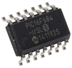
Break IC PIC16F684 Binary
Let’s get some knowledge about PIC16F684 to better Break IC PIC16F684 Binary
14-Pin Flash-Based, 8-Bit CMOS Microcontrollers with nanoWatt Technology
High-Performance RISC CPU:
· Only 35 instructions to learn:
– All single-cycle instructions except branches
· Operating speed:
– DC – 20 MHz oscillator/clock input
– DC – 200 ns instruction cycle
· Interrupt capability
· 8-level deep hardware stack
Break IC PIC16F684 Binary
· Direct, Indirect and Relative Addressing modes
Special Microcontroller Features:
· Precision Internal Oscillator:
– Factory calibrated to ±1%
– Software selectable frequency range of 8 MHz to 31 kHz
– Software tunable
– Two-speed Start-up mode which is useful for Break IC PIC16F616 Heximal
– Crystal fail detect for critical applications
– Clock mode switching during operation for power savings
· Power-saving Sleep mode
· Wide operating voltage range (2.0V-5.5V)
· Industrial and Extended Temperature range
· Power-on Reset (POR)
· Power-up Timer (PWRT) and Oscillator Start-up Timer (OST)
· Brown-out Detect (BOD) with software control option
· Enhanced low-current Watchdog Timer (WDT) with on-chip oscillator (software selectable nominal 268 seconds with full prescaler) with software enable
· Multiplexed Master Clear with pull-up/input pin
· Programmable code protection is one of the application for Break IC PIC12F609 Heximal
· High Endurance Flash/EEPROM cell:
– 100,000 write Flash endurance
– 1,000,000 write EEPROM endurance
– Flash/Data EEPROM retention: > 40 years
Peripheral Features:
· 12 I/O pins with individual direction control:
– High current source/sink for direct LED drive in the end
– Interrupt-on-pin change
– Individually programmable weak pull-ups
– Ultra Low-power Wake-up (ULPWU)
· Analog comparator module with:
– Two analog comparators
– Programmable on-chip voltage reference (CVREF) module (% of VDD)
– Comparator inputs and outputs externally accessible
· A/D Converter:
– 10-bit resolution and 8 channels
· Timer0: 8-bit timer/counter with 8-bit programmable prescaler
· Enhanced Timer1:
– 16-bit timer/counter with prescaler
– External Gate Input mode
– Option to use OSC1 and OSC2 in LP mode as Timer1 oscillator if INTOSC mode selected
· Timer2: 8-bit timer/counter with 8-bit period register, prescaler and postscaler
· Enhanced Capture, Compare, PWM module:
– 16-bit Capture, max resolution 12.5 ns
– Compare, max resolution 200 ns
– 10-bit PWM with 1, 2 or 4 output channels, programmable “dead time”, max frequency 20 kHz
· In-Circuit Serial ProgrammingTM (ICSPTM) via two pins
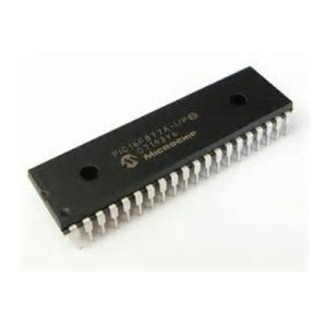
Break IC PIC16F877A Heximal
The data EEPROM and Flash program memory is readable after Break IC PIC16F877A Heximal and writable during normal operation (over the full VDD range). This memory is not directly mapped in the register file space. Instead, it is indirectly addressed through the Special Function Registers. There are six SFRs used to read and write this memory:
EECON1
EECON2
EEDATA
EEDATH
EEADR
EEADRH
When interfacing to the data memory block, EEDATA holds the 8-bit data for read/write and EEADR holds the address of the EEPROM location being accessed. These devices have 128 or 256 bytes of data EEPROM (depending on the device), with an address range from 00h to FFh. On devices with 128 bytes, addresses from 80h to FFh are unimplemented and will wraparound to the beginning of data EEPROM memory to facilitate the process of Break IC PIC12F635 Program. When writing to unimplemented locations, the on-chip charge pump will be turned off.
When interfacing the program memory block, the EEDATA and EEDATH registers form a two-byte word that holds the 14-bit data for read/write and the EEADR and EEADRH registers form a two-byte word that holds the 13-bit address of the program memory location being accessed.
Break IC PIC16F877A Heximal
These devices have 4 or 8K words of program Flash, with an address range from 0000h to 0FFFh for the PIC16F873A/874A and 0000h to 1FFFh for the PIC16F876A/877A. Addresses above the range of the respective device will wraparound to the beginning of program memory.
The EEPROM data memory allows single-byte read and write. The Flash program memory allows single-word reads and four-word block writes.
Program memory write operations automatically perform an erase-before-write on blocks of four words. A byte write in data EEPROM memory automatically erases the location and writes the new data (erase-before-write) in order to Attack MCU PIC16F630 Firmware.
The write time is controlled by an on-chip timer. The write/erase voltages are generated by an on-chip charge pump, rated to operate over the voltage range of the device for byte or word operations. When the device is code-protected, the CPU may continue to read and write the data EEPROM memory.
Depending on the settings of the write-protect bits, the device may or may not be able to write certain blocks of the program memory; however, reads of the program memory are allowed. When code-protected, the device programmer can no longer access data or program for the purpose of Microcontroller Unlocking.
Break IC PIC16F876A Binary
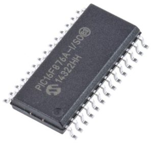
There are three memory blocks in each of the PIC16F87XA devices, the hacker who is preparing Break IC PIC16F876A Binary needs to understand this. The program memory and data memory have separate buses so that concurrent access can occur and is detailed in this section. The EEPROM data memory block is detailed in Section 3.0.
“Data EEPROM and Flash Program Memory”. Additional information on device memory may be found in the PICmicro® Mid-Range MCU Family Reference Manual (DS33023)
PROGRAM MEMORY ORGANIZATION
The PIC16F87XA devices have a 13-bit program counter capable of addressing an 8K word x 14 bit program memory space. The PIC16F876A/877A devices have 8K words x 14 bits of Flash program memory, while PIC16F873A/874A devices have 4K words x 14 bits. Accessing a location above the physically implemented address will cause a wraparound
Break IC PIC16F876A Binary
The Reset vector is at 0000h and the interrupt vector is at 0004h.
DATA MEMORY ORGANIZATION
The data memory is partitioned into multiple banks which contain the General Purpose Registers and the Special Function Registers. Bits RP1 (Status<6>) and RP0 (Status<5>) are the bank select bits.
Each bank extends up to 7Fh (128 bytes). The lower locations of each bank are reserved for the Special Function Registers. Above the Special Function Registers are General Purpose Registers, implemented as static RAM. All implemented banks contain Special Function Registers. Some frequently used Special Function Registers from one bank may be mirrored in another bank for code reduction and quicker access for the purpose of Copy Microcontroller PIC16F639 Heximal.
The Special Function Registers are registers used by the CPU and peripheral modules for controlling the desired operation of the device. These registers are implemented as static RAM.
The Special Function Registers can be classified into two sets: core (CPU) and peripheral. Those registers associated with the core functions are described in detail in this section to faciliate the process of Break Chip PIC16F785 Heximal. Those related to the operation of the peripheral features are described in detail in the peripheral features section.
Break IC PIC16F874A Software
Acquained with CMOS Technology can greatly help to Break IC PIC16F874A Software:
· Low-power, high-speed Flash/EEPROM technology
· Fully static design
· Wide operating voltage range (2.0V to 5.5V)
· Commercial and Industrial temperature ranges
· Low-power consumption
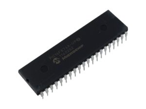
PIC16F874A devices are available only in 28-pin packages, while PIC16F874A/877A devices are available in 40-pin and 44-pin packages. All devices in the PIC16F87XA family share common architecture with the following differences:
· The PIC16F873A and PIC16F874A have one-half of the total on-chip memory of the PIC16F876A and PIC16F877A
· The 28-pin devices have three I/O ports, while the 40/44-pin devices have five
· The 28-pin devices have fourteen interrupts, while the 40/44-pin devices have fifteen for the purpose
· The 28-pin devices have five A/D input channels, while the 40/44-pin devices have eight
· The Parallel Slave Port is implemented only on the 40/44-pin devices
Break IC PIC16F874A Software
The available features are summarized in Table 1-1. Block diagrams of the PIC16F873A/876A and PIC16F874A/877A devices are provided in Figure 1-1 and Figure 1-2, respectively.
The pinouts for these device families are listed in Table 1-2 and Table 1-3. Additional information may be found in the PICmicro Mid-Range Reference Manual (DS33023), which may be obtained from your local Microchip Sales Representative or downloaded from the Microchip web site.
The Reference Manual should be considered a complementary document to this data sheet and is highly recommended reading for a better understanding of the device architecture and operation of the peripheral modules.
Break IC PIC16F873A Code
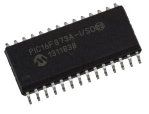
Below we will introduce some basic features of PIC16F873A which will be useful for Break IC PIC16F873A Code
High-Performance RISC CPU:
· Only 35 single-word instructions to learn
· All single-cycle instructions except for program branches, which are two-cycle
· Operating speed: DC – 20 MHz clock input DC – 200 ns instruction cycle
· Up to 8K x 14 words of Flash Program Memory,
Up to 368 x 8 bytes of Data Memory (RAM),
Up to 256 x 8 bytes of EEPROM Data Memory
· Pinout compatible to other 28-pin or 40/44-pin PIC16CXXX and PIC16FXXX microcontrollers
Peripheral Features:
· Timer0: 8-bit timer/counter with 8-bit prescaler
· Timer1: 16-bit timer/counter with prescaler, can be incremented during Sleep via external crystal/clock
· Timer2: 8-bit timer/counter with 8-bit period register, prescaler and postscaler
Break IC PIC16F873A Code
· Two Capture, Compare, PWM modules
– Capture is 16-bit, max. resolution is 12.5 ns
– Compare is 16-bit, max. resolution is 200 ns
– PWM max. resolution is 10-bit
· Synchronous Serial Port (SSP) with SPI™ for the purpose
(Master mode) and I2C™ (Master/Slave)
· Universal Synchronous Asynchronous Receiver Transmitter (USART/SCI) with 9-bit address detection which can be used for Break MCU PIC18F442 Software
· Parallel Slave Port (PSP) – 8 bits wide with external RD, WR and CS controls (40/44-pin only)
· Brown-out detection circuitry for Brown-out Reset (BOR)
· Analog Comparator module with:
– Two analog comparators
– Programmable on-chip voltage reference (VREF) module
– Programmable input multiplexing from device inputs and internal voltage reference
– Comparator outputs are externally accessible
Special Microcontroller Features:
· 100,000 erase/write cycle Enhanced Flash program memory typical
· 1,000,000 erase/write cycle Data EEPROM memory typical
· Data EEPROM Retention > 40 years which is a very important point for Recover MCU PIC16F874 Code
· Self-reprogrammable under software control
· In-Circuit Serial Programming™ (ICSP™) via two pins
· Single-supply 5V In-Circuit Serial Programming
· Watchdog Timer (WDT) with its own on-chip RC oscillator for reliable operation
· Programmable code protection
· Power saving Sleep mode
· Selectable oscillator options
· In-Circuit Debug (ICD) via two pins Serial Port (SSP) with SPI™
(Master mode) and I2C™ (Master/Slave)
· Universal Synchronous Asynchronous Receiver Transmitter (USART/SCI) with 9-bit address detection
· Parallel Slave Port (PSP) – 8 bits wide with external RD, WR and CS controls (40/44-pin only)
· Brown-out detection circuitry for Brown-out Reset (BOR) which can ease the process of MCU Cracking.
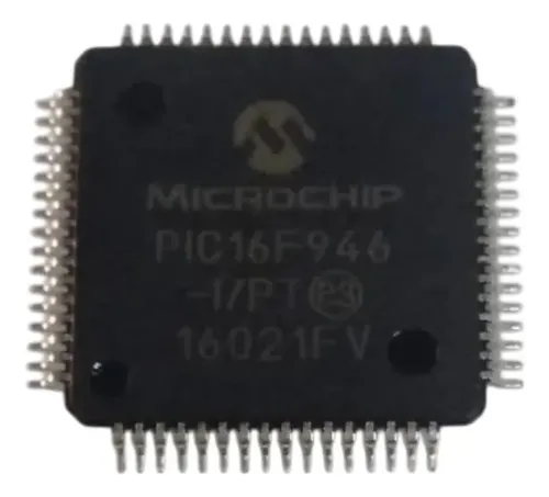
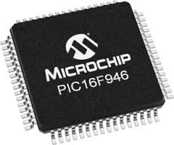
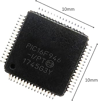
Break MCU PIC16F946 Program
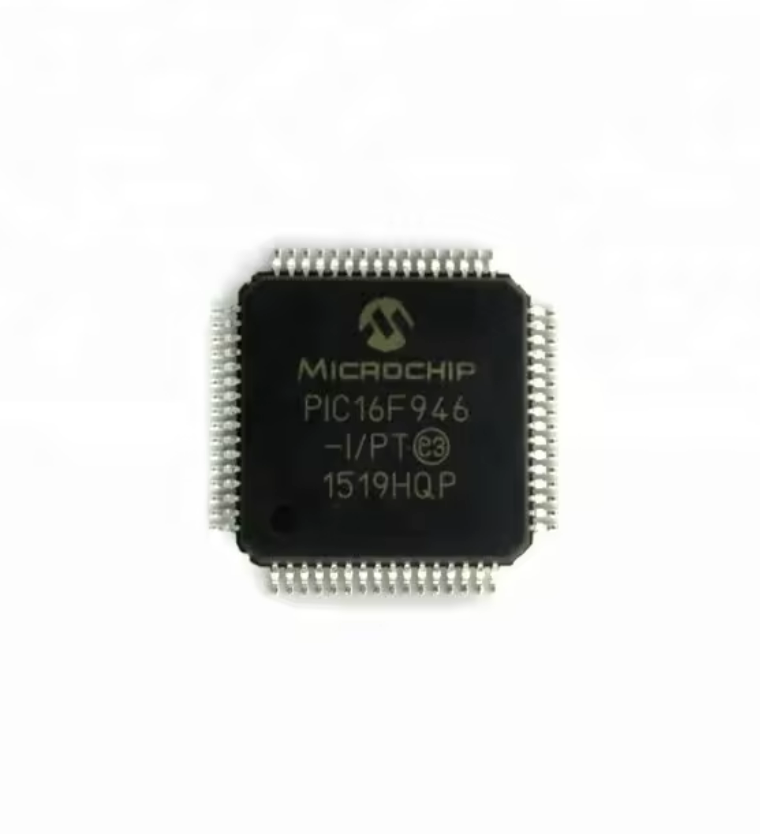
The PIC16F946 microcontroller is a highly integrated embedded MCU widely used in intelligent control systems that require stable performance, low power consumption, and compact hardware architecture. This device is frequently found in industrial automation platforms, medical electronics, instrumentation systems, security products, consumer appliances, and automotive control modules. With built-in peripheral functions and configurable internal memory, the PIC16F946 can store complex operational firmware, application program routines, and critical data archives directly within the chip. In commercial applications, manufacturers often configure the MCU as protected, locked, or encrypted in order to secure proprietary source code, binary, and heximal files against unauthorized access. However, when original development resources are unavailable, recovering these valuable assets becomes essential for maintenance and product continuity.
The AUSART will remain active during Sleep only in the Synchronous Slave mode. All other modes require the system clock and therefore cannot generate the necessary signals to run the Transmit or Receive Shift registers during Sleep.
Synchronous Slave mode uses an externally generated clock to run the Transmit and Receive Shift registers.
9.4.1 SYNCHRONOUS RECEIVE DURING SLEEP
To receive during Sleep, all the following conditions must be met before entering Sleep mode:
· RCSTA and TXSTA Control registers must be configured for Synchronous Slave Reception.
· If interrupts are desired, set the RCIE bit of the PIE1 register and the PEIE bit of the INTCON register.
Upon entering Sleep mode, the device will be breaky to accept data and clocks on the RX/DT and TX/CK pins, respectively. When the data word has been completely clocked in by the external device, the RCIF interrupt flag bit of the PIR1 register will be set. Thereby, waking the processor from Sleep.
Upon waking from Sleep, the instruction following the SLEEP instruction will be executed. If the GIE global interrupt enable bit of the INTCON register is also set, then the Interrupt Service Routine at address 004h will be called.
9.4.2 SYNCHRONOUS TRANSMIT DURING SLEEP
To transmit during Sleep, all the following conditions must be met before entering Sleep mode:
· RCSTA and TXSTA Control registers must be configured for Synchronous Slave Transmission (see Section 9.3.2.2 “Synchronous Slave Transmission Set-up:”).
· The TXIF interrupt flag must be cleared by writing the output data to the TXREG, thereby filling the TSR and transmit buffer. If interrupts are desired, set the TXIE bit of the PIE1 register and the PEIE bit of the INTCON register. Upon entering Sleep mode, the device will be breaky to accept clocks on TX/CK pin and transmit data on the RX/DT pin. When the data word in the TSR has been completely clocked out by the external device, the pending byte in the TXREG will transfer to the TSR and the TXIF flag will be set. Thereby, waking the processor from Sleep. At this point, the TXREG is available to accept another character for transmission, which will clear the TXIF flag.
Our “Break MCU PIC16F946 Program” service provides advanced solutions to attack, break, and decode these highly secured microcontrollers while maintaining maximum integrity of the original embedded data. Through precision decapsulate operations, voltage fault analysis, and proprietary extraction procedures, our engineers are able to retrieve hidden firmware, reconstruct damaged binary archives, and recover complete heximal program files from internal flash, EEPROM, and protected memory areas. Even if the device incorporates sophisticated protective mechanisms or multiple layers of encrypted storage, we apply specialized methods to effectively hack through these restrictions and obtain accurate source code representations. Once extracted, the recovered data files can be used to clone, duplicate, migrate, or restore existing products without requiring a complete redesign of the hardware platform.
Upon waking from Sleep, the instruction following the SLEEP instruction will be executed. If the GIE global interrupt enable bit is also set then the Interrupt Service Routine at address 0004h.
The technical process behind this service combines physical semiconductor analysis with advanced logical reconstruction. During the decapsulation stage, the package is carefully opened to expose the silicon die and allow direct interaction with internal circuitry. This enables low-level retrieval of embedded memory structures and facilitates extraction of raw binary and heximal content. Afterward, sophisticated decode algorithms analyze the collected data archive, organizing fragmented firmware files into coherent program structures suitable for engineering analysis. Our specialists then validate the extracted source code to ensure operational consistency with the original MCU behavior. By combining invasive and non-invasive methodologies, we are able to overcome many forms of locked and secured protection systems commonly implemented in legacy and modern PIC microcontrollers.
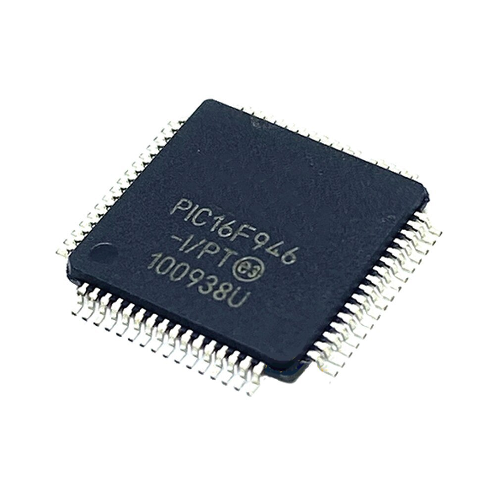
For manufacturers, maintenance providers, and engineering companies, the ability to recover PIC16F946 firmware offers major operational and commercial advantages. Access to original program files allows organizations to extend product life cycles, repair discontinued equipment, and maintain compatibility with legacy systems. Instead of investing significant time and cost into redevelopment, customers can utilize our service to attack, decode, and reconstruct protected memory data efficiently. The recovered binary archives and source code also support product migration, redesign optimization, and hardware replication projects. Through our expertise in breaking, retrieving, and duplicating secured MCU environments, we help clients regain control over critical electronic assets and preserve valuable technological resources for future development.
Break IC PIC12F629 Program
Break IC PIC12F629 Program
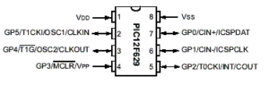
Break IC PIC12F629 Program from its memory needs to decapsulate its silicon layer as well as metal layer, use probe to get access to the internal wafer die for databus probing:
High-Performance RISC CPU:
· Only 35 Instructions to Learn
– All single-cycle instructions except branches
· Operating Speed:
– DC – 20 MHz oscillator/clock input
– DC – 200 ns instruction cycle
· Interrupt Capability
· 8-Level Deep Hardware Stack
· Direct, Indirect, and Relative Addressing modes
Break IC PIC12F629 Program
Special Microcontroller Features:
· Internal and External Oscillator Options
– Precision Internal 4 MHz oscillator factory calibrated to ±1%
– External Oscillator support for crystals and resonators
– 5 ms wake-up from Sleep, 3.0V, typical
· Power-Saving Sleep mode
· Wide Operating Voltage Range – 2.0V to 5.5V
· Industrial and Extended Temperature Range
· Low-Power Power-on Reset (POR)
· Power-up Timer (PWRT) and Oscillator Start-up Timer (OST)
· Brown-out Detect (BOD)
· Watchdog Timer (WDT) with Independent Oscillator for Reliable Operation
· Multiplexed MCLR/Input Pin
· Interrupt-on-Pin Change
· Individual Programmable Weak Pull-ups
· Programmable Code Protection
· High Endurance Flash/EEPROM Cell
– 100,000 write Flash endurance
– 1,000,000 write EEPROM endurance
– Flash/Data EEPROM Retention: > 40 years
Low-Power Features:
· Standby Current:
– 1 nA @ 2.0V, typical
· Operating Current:
– 8.5 mA @ 32 kHz, 2.0V, typical
– 100 mA @ 1 MHz, 2.0V, typical
· Watchdog Timer Current
– 300 nA @ 2.0V, typical
· Timer1 Oscillator Current:
– 4 mA @ 32 kHz, 2.0V, typical
Peripheral Features:
· 6 I/O Pins with Individual Direction Control
· High Current Sink/Source for Direct LED Drive
· Analog Comparator module with:
– One analog comparator
– Programmable on-chip comparator voltage reference (CVREF) module
– Programmable input multiplexing from device inputs
– Comparator output is externally accessible
· Analog-to-Digital Converter module (PIC12F675):
– 10-bit resolution
– Programmable 4-channel input
– Voltage reference input
· Timer0: 8-Bit Timer/Counter with 8-Bit Programmable Prescaler
· Enhanced Timer1:
– 16-bit timer/counter with prescaler
– External Gate Input mode
– Option to use OSC1 and OSC2 in LP mode as Timer1 oscillator, if INTOSC mode selected
· In-Circuit Serial ProgrammingTM (ICSPTM) via two pins through CRACK MCU
Break IC PIC12F639 Heximal
Break IC PIC12F639 Heximal
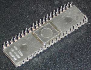
Break IC PIC12F639 Heximal from its memory needs to know its memory organization
PROGRAM MEMORY ORGANIZATION
The PIC16F639 devices have a 13-bit program counter capable of addressing an 8K x 14 program memory space. Only the first 1K x 14 (0000h-03FFh, for the PIC12F635) and 2K x 14 (0000h-07FFh, for the PIC16F636/639) is physically implemented. Accessing a location above these boundaries will cause a wrap around within the first 2K x 14 space. The Reset vector is at 0000h and the interrupt vector is at 0004h.
DATA MEMORY ORGANIZATION
The data memory (see below Figure) is partitioned into two banks, which contain the General Purpose Registers (GPR) and the Special Function Registers (SFR).
The Special Function Registers are located in the first 32 locations of each bank. Register locations 20h-7Fh in Bank 0 and A0h-BFh in Bank 1 are GPRs, implemented as static RAM for the PIC16F639.For the PIC12F635, register locations 40h through 7Fh are GPRs implemented as static RAM. Register locations F0h-FFh in Bank 1 point to addresses 70h-7Fh in Bank 0. All other RAM is unimplemented and returns ‘0’ when read. RP0 (STATUS<5>) is the bank select bit.
GENERAL PURPOSE REGISTER
The register file is organized as 64 x 8 for the PIC12F635 and 128 x 8 for the PIC16F636/639. Each register is accessed, either directly or indirectly, through the File Select Register;
Break IC PIC12F639 Heximal
SPECIAL FUNCTION REGISTERS
The Special Function Registers (SFRs) are registers used by the CPU and peripheral functions for controlling the desired operation of the device. These registers are static RAM. The special registers can be classified into two sets: core and peripheral. The Special Function Registers associated with the “core” are described in this section. Those related to the operation of the peripheral features are described in the section of that peripheral feature from MCU CRACK.
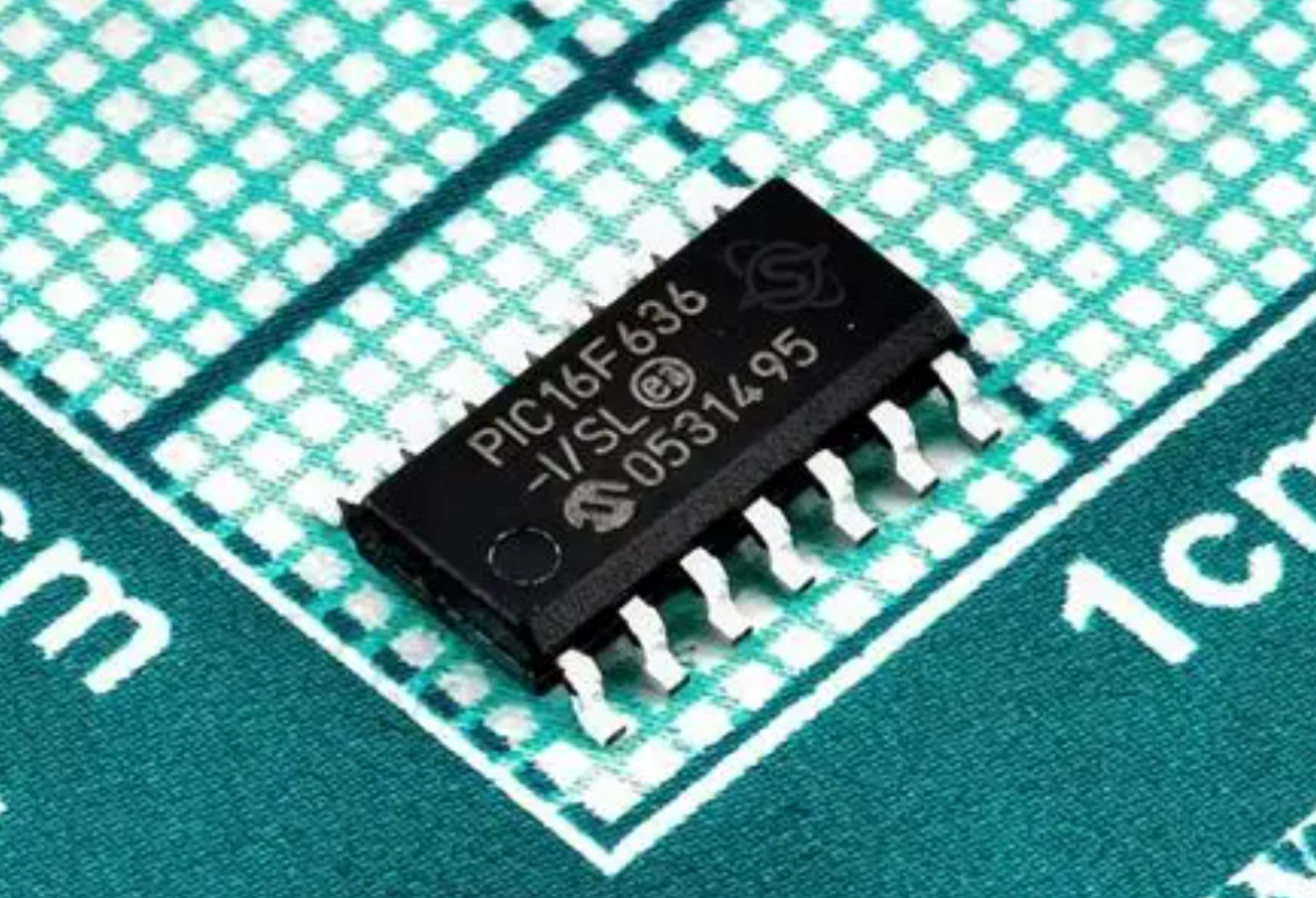
Break IC PIC16F636 Code
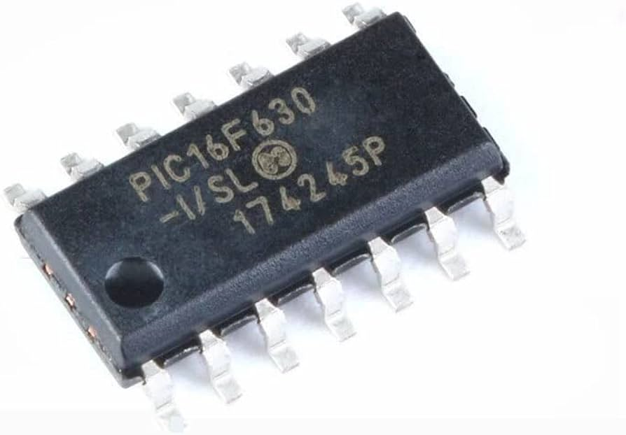
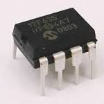
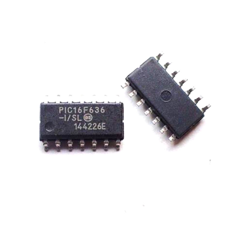
The PIC16F636 is a highly versatile, embedded MCU renowned for its robust protective features, including locked flash and encrypted EEPROM sections. Widely adopted in automotive body controls, consumer electronics, industrial timers, and medical alert systems, this chip manages critical operations where reliability is non-negotiable. Its unique 14-bit core, integrated comparator module, and programmable memory architecture allow engineers to store firmware that governs everything from LED lighting sequences to sensor data logging. However, when original source code or binary files are lost due to obsolete tools, unavailable archives, or legacy product maintenance needs, a legitimate requirement emerges: to break through the chip’s own secured perimeter not for malice, but for recovery, analysis, or compatibility upgrades.
Peripheral Features:
· 6/12 I/O pins with individual direction control:
– High-current source/sink for direct LED drive
– Interrupt-on-pin change
– Individually programmable weak pull-ups/pull-downs
– Ultra Low-Power Wake-up
· Analog comparator module with:
– Up to two analog comparators
– Programmable on-chip voltage reference (CVREF) module (% of VDD)
– Comparator inputs and outputs externally accessible
· Timer0: 8-bit timer/counter with 8-bit programmable prescaler
· Enhanced Timer1:
– 16-bit timer/counter with prescaler
– External Gate Input mode
– Option to use OSC1 and OSC2 in LP mode as Timer1 oscillator if INTOSC mode selected
· KEELOQ® compatible hardware Cryptographic module
· In-Circuit Serial ProgrammingTM (ICSPTM) via two pins
Low Frequency Analog Front-End Features (PIC16F639 only)
· Three input pins for 125 kHz LF input signals
· High input detection sensitivity (3 mVPP, typical)
· Demodulated data, Carrier clock or RSSI output selection
· Input carrier frequency: 125 kHz, typical
· Input modulation frequency: 4 kHz, maximum
· 8 internal configuration registers
· Bidirectional transponder communication (LF talk back)
· Programmable antenna tuning capacitance (up to 63 pF, 1 pF/step)
· Low standby current: 5 ìA (with 3 channels enabled), typical
· Low operating current: 15 ìA (with 3 channels enabled), typical
· Serial Peripheral Interface (SPI™) with internal MCU and external devices
· Supports Battery Back-up mode and batteryless operation with external circuits ly LOQ® compatible hardware Cryptographic module
· In-Circuit Serial ProgrammingTM (ICSPTM) IC breakion;
To attack the protected silicon directly, specialists first perform decapsulate – chemically removing the epoxy resin that shields the die. Under microscopic examination, focused ion beam (FIB) workarounds or low-level voltage glitching can hack the flash reading protection, allowing engineers to retrieve the raw heximal (Intel HEX format) file from memory. Another common method uses side-channel analysis to decode instruction sequences without triggering hardware locks. Once the data is extracted, technicians clone the entire MCU configuration – including eeprom calibration values and program counters – onto a new chip. Alternatively, they duplicate the archive into a software emulator, enabling firmware verification or behavioral modification. These processes require expensive labs and deep understanding of microarchitecture, which is why our service exists: to ethically break locked chips for clients who own the original hardware but cannot access its binary logic.
DEVICE OVERVIEW
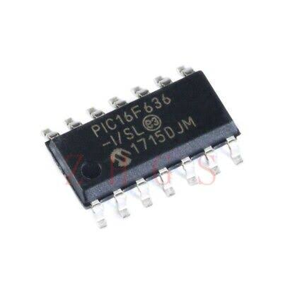
This document contains device specific information for the PIC12F635/PIC16F636/639 devices. Additional information may be found in the “PICmicro® Mid-Range MCU Family Reference Manual” (DS33023), which may be obtained from your local Microchip Sales Representative or downloaded from the Microchip web site. The reference manual should be considered a complementary document to this data sheet and is highly recommended reading for a better understanding of the device architecture and operation of the peripheral modules.
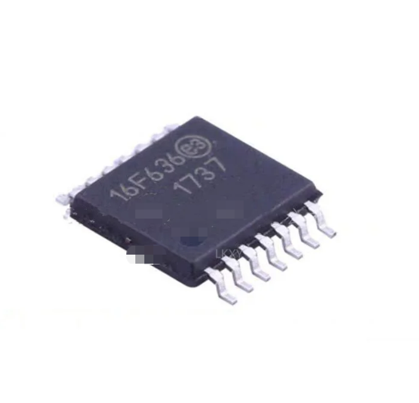
Our core purpose is to hack through encrypted barriers only after verifying legal ownership. The primary benefit is avoiding total system obsolescence. Consider an industrial conveyor controller built around the PIC16F636: if the sole source code was lost in a server crash, production lines would freeze. By allowing us to decapsulate and retrieve the firmware, you receive a complete archive of flash and eeprom content, which can be cloned onto replacement MCUs or duplicated for backup. Similarly, medical devices with secured but outdated logic can be decoded to improve safety patches without redesigning certified hardware. The data we recover remains bit-perfect – preserving timings, interrupt vectors, and trim values that generic heximal files often miss. End users gain a second life for embedded products, reduce e-waste, and circumvent expensive redesigns. Our service transforms a locked silicon puzzle into an open program that you control again, legally and efficiently.