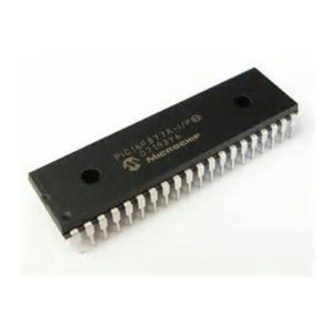
 Break IC PIC16F877A Heximal
The data EEPROM and Flash program memory is readable after Break IC PIC16F877A Heximal and writable during normal operation (over the full VDD range). This memory is not directly mapped in the register file space. Instead, it is indirectly addressed through the Special Function Registers. There are six SFRs used to read and write this memory:
EECON1
EECON2
EEDATA
EEDATH
EEADR
EEADRH
When interfacing to the data memory block, EEDATA holds the 8-bit data for read/write and EEADR holds the address of the EEPROM location being accessed. These devices have 128 or 256 bytes of data EEPROM (depending on the device), with an address range from 00h to FFh. On devices with 128 bytes, addresses from 80h to FFh are unimplemented and will wraparound to the beginning of data EEPROM memory to facilitate the process of Break IC PIC12F635 Program. When writing to unimplemented locations, the on-chip charge pump will be turned off.
When interfacing the program memory block, the EEDATA and EEDATH registers form a two-byte word that holds the 14-bit data for read/write and the EEADR and EEADRH registers form a two-byte word that holds the 13-bit address of the program memory location being accessed.

Break IC PIC16F877A Heximal
These devices have 4 or 8K words of program Flash, with an address range from 0000h to 0FFFh for the PIC16F873A/874A and 0000h to 1FFFh for the PIC16F876A/877A. Addresses above the range of the respective device will wraparound to the beginning of program memory.
The EEPROM data memory allows single-byte read and write. The Flash program memory allows single-word reads and four-word block writes.
Program memory write operations automatically perform an erase-before-write on blocks of four words. A byte write in data EEPROM memory automatically erases the location and writes the new data (erase-before-write) in order to Attack MCU PIC16F630 Firmware.
The write time is controlled by an on-chip timer. The write/erase voltages are generated by an on-chip charge pump, rated to operate over the voltage range of the device for byte or word operations. When the device is code-protected, the CPU may continue to read and write the data EEPROM memory.
Depending on the settings of the write-protect bits, the device may or may not be able to write certain blocks of the program memory; however, reads of the program memory are allowed. When code-protected, the device programmer can no longer access data or program for the purpose of Microcontroller Unlocking.