Archive for the ‘Break IC’ Category
 Break IC PIC16F621A Program
 February 27th, 2015 |
  Author:
 The PIC16C621A microcontroller remains a staple in industrial automation, automotive control modules, consumer electronics, and lighting systems due to its robust 8-bit RISC architecture, high-current LED drive capability, and dual analog comparators. This legacy CMOS microcontroller stores critical, time-tested logic within its internal configuration. However, manufacturers frequently face immense production bottlenecks when a legacy system requires updates, but the original source code is lost to time, or the primary supplier goes out of business. To prevent a complete and costly system redesign, engineering teams must find a reliable path to extract and preserve their embedded logic. Our specialized engineering services offer a safe, reliable process to break IC PIC16C621A program architectures, giving you a fresh opportunity to revive, update, or safeguard your valuable hardware investments.
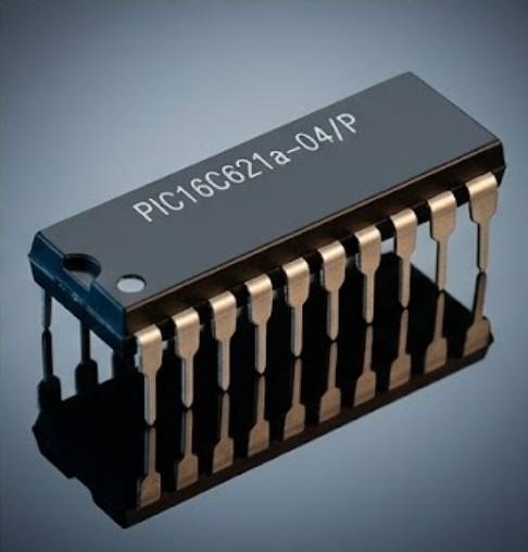
UV Erasable Devices
The UV erasable version, offered in CERDIP package is optimal for prototype development and pilot programs. This version can be erased and reprogrammed to any of the oscillator modes. Microchip’s PICSTART® and PRO MATE® programmers both support programming of the PIC16C62X.
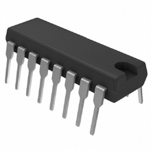
One-Time-Programmable (OTP) Devices
The availability of OTP devices is especially useful for customers who need the flexibility for frequent code updates and small volume applications. In addition to the program memory, the configuration bits must also be programmed.
QUICK TURNAROUND PRODUCTION
Microchip offers a QTP Programming Service for factory production orders. This service is made available for users who chose not to program a medium to high quantity of units and whose code patterns have stabilized. The devices are identical to the OTP devices but with all EPROM locations and configuration options already programmed by the factory. Certain code and prototype verification procedures apply before production shipments are available. Microchip offers a unique programming service where a few user-defined locations in each device are programmed with different serial numbers. The serial numbers may be random, pseudo-random or sequential. Serial programming allows each device to have a unique number which can serve as an entry-code, password or ID number.
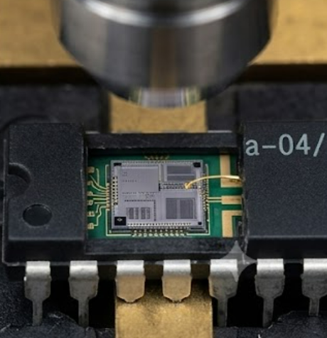
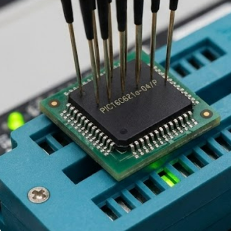
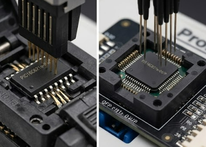
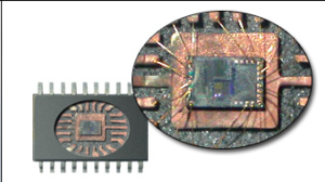
When a manufacturer ships a finished product, the controller is typically treated as a secured, locked environment to prevent unapproved tampering. Overriding this protective framework requires highly advanced laboratory techniques. To bypass these embedded security constraints, our technicians first decapsulate the outer physical packaging of the microcontroller to expose the raw silicon die underneath. Once the internal structures are visible, we use precision micro-probing to safely modify the internal state of the hardware. This temporary modification allows us to safely bypass the original protective code fuses without destroying the underlying architecture. By isolating the internal memory sectors, our technical experts can seamlessly extract the raw binary data. This highly targeted procedure allows us to decode the architecture, break the lock mechanisms, and retrieve a flawless heximal file representing the original machine instructions.
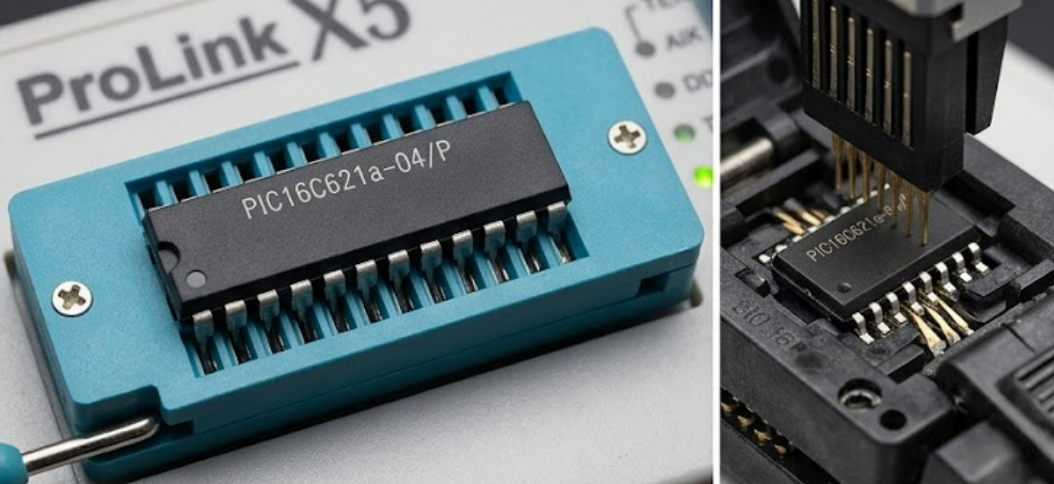
Why Engineering Teams Choose to Clone and Modify Legacy Firmware
The core purpose of opting to decode or hack into a tightly secured microcontroller is rarely about starting from scratch; rather, it is about maintaining operational continuity and extracting maximum value from established assets. Companies utilize our expert engineering solutions to reverse-engineer out-of-production systems, perform detailed competitive analysis, or update firmware when original source code files are entirely missing. Whether the target logic is stored in older EPROM, flash, or peripheral PLD matrices, our team can extract the complete data set. Once we successfully retrieve the core application, engineers can easily duplicate the functional parameters onto a modern, equivalent circuit. This process ensures you can seamlessly clone the device behavior and compile a verified archive, making sure your machinery keeps running without experiencing a single day of unexpected downtime.
Direct Benefits for the End User: Security, Stability, and Continuity
Partnering with an experienced team to break, attack, and extract locked hardware logic provides major technical and financial benefits to end users and product managers alike. Instead of devoting months of expensive engineering time to completely re-coding an embedded system from scratch—which invariably introduces fresh programming bugs—our laboratory provides a direct pipeline to a functional, verified binary file. This structural continuity ensures your newly produced duplicate boards behave exactly like the original field units. Our custom extraction service effectively eliminates the typical supply chain risks associated with obsolete chips, safeguards your intellectual property from losing its utility, and gives you a stable, long-term foundation to manage your hardware deployments smoothly for decades to come.
 Posted in
Break IC PIC12F635 Program
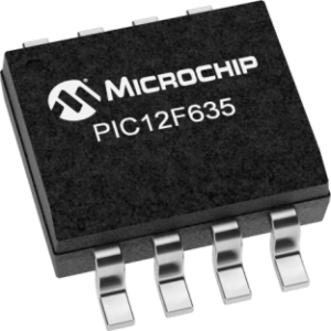
We can break IC PIC12F635 Program, please view the PIC12F635 features for your reference:
High-Performance RISC CPU:
· Only 35 instructions to learn:
– All single-cycle instructions except branches
· Operating speed:
– DC – 20 MHz oscillator/clock input
– DC – 200 ns instruction cycle
· Interrupt capability
· 8-level deep hardware stack
· Direct, Indirect and Relative Addressing modes
Special Microcontroller Features:
· Precision Internal Oscillator:
– Factory calibrated to ±1%
– Software selectable frequency range of 8 MHz to 31 kHz
– Software tunable
– Two-Speed Start-up mode
– Crystal fail detect for critical applications
· Clock mode switching for low power operation
· Power-saving Sleep mode
· Wide operating voltage range (2.0V-5.5V)
· Industrial and Extended Temperature range
· Power-on Reset (POR)
· Wake-up Reset (WUR)
Break IC PIC12F635 Program
· Independent weak pull-up/pull-down resistors
· Programmable Low-Voltage Detect (PLVD)
· Power-up Timer (PWRT) and Oscillator Start-up Timer (OST)
· Brown-out Detect (BOD) with software control option
· Enhanced Low-Current Watchdog Timer (WDT) with on-chip oscillator (software selectable nominal 268 seconds with full prescaler) with software enable
· Multiplexed Master Clear with pull-up/input pin
· Programmable code protection (program and data independent)
· High-Endurance Flash/EEPROM cell to crack MCU
– 100,000 write Flash endurance
– 1,000,000 write EEPROM endurance
– Flash/Data EEPROM Retention: > 40 years for the purpose of break IC PIC12F635 Program
Low Power Features:
· Standby Current:
– 1 nA @ 2.0V, typical
· Operating Current:
– 8.5 ìA @ 32 kHz, 2.0V, typical
– 100 ìA @ 1 MHz, 2.0V, typical
· Watchdog Timer Current:
– 1 ìA @ 2.0V, typical
Break IC PIC12F609 Flash Heximal
Break IC PIC12F609 Flash Heximal means the flash memory will have to set up as unlock status, in order to do that we must have an clear idea about its organization:
Program Memory Organization
The PIC12F609 has a 13-bit program counter capable of addressing an 8K x 14 program memory space. Only the first 1K x 14 (0000h-03FFh) for the PIC12F609 is physically implemented. Accessing a location above these boundaries will cause a wraparound within the first 1K x 14 space. The Reset vector is at 0000h and the interrupt vector is at 0004h.
Break IC PIC12F609 Flash Heximal
Data Memory Organization
The data memory (see Figure 2-2) is partitioned into two banks, which contain the General Purpose Registers (GPR) and the Special Function Registers (SFR). The Special Function Registers are located in the first 32 locations of each bank. Register locations 40h-7Fh in Bank 0 are General Purpose Registers, implemented as static RAM. Register locations F0h-FFh in Bank 1 point to addresses 70h-7Fh in Bank 0. All other RAM is unimplemented and returns ‘0’ when read. The RP0 bit of the STATUS register is the bank select bit.
The Special Function Registers are registers used by the CPU and peripheral functions for controlling the desired operation of the device. These registers are static RAM which can be manipulated by Recover MCU PIC16F877 Program.
The special registers can be classified into two sets: core and peripheral. The Special Function Registers associated with the “core” are described in this section. Those related to the operation of the peripheral features are described in the section of that peripheral feature.
The STATUS register, shown in Register 2-1, contains:
· the arithmetic status of the ALU
· the Reset status
· the bank select bits for data memory (RAM)
The STATUS register can be the destination for any instruction, like any other register. If the STATUS register is the destination for an instruction that affects the Z, DC or C bits, then the write to these three bits is disabled. These bits are set or cleared according to the device logic in order to Break IC PIC16F876A Binary. Furthermore, the TO and PD bits are not writable. Therefore, the result of an instruction with the STATUS register as destination may be different than intended for the purpose of Break IC PIC12F609 Flash Heximal.
Break IC PIC16F616 Heximal
Break IC PIC16F616 Heximal starts from get some knowledge about its structure:
PIC16F616/16HV616 only:
· A/D Converter:
– 10-bit resolution
– 8 external input channels
– 2 internal reference channels
· Timer2: 8-bit timer/counter with 8-bit period register, prescaler and postscaler
· Enhanced Capture, Compare, PWM module:
– 16-bit Capture, max. resolution 12.5 ns
– 16-bit Compare, max. resolution 200 ns
– 10-bit PWM with 1, 2 or 4 output channels, programmable “dead time”, max. frequency 20 kHz
Program Memory Organization of PIC16F616/16HV616
The PIC16F610/616/16HV610/616 has a 13-bit program counter capable of addressing an 8k x 14 program memory space. Only the first 1K x 14 (0000h-3FF) for the PIC16F610/16HV610 and the first 2K x 14 (0000h-07FFh) for the PIC16F616/16HV616 is physically implemented to facilitate the process of Recover MCU PIC16F648A Firmware.
Accessing a location above these boundaries will cause a wraparound within the first 1K x 14 space (PIC16F610/16HV610) and 2K x 14 space (PIC16F616/16HV616). The Reset vector is at 0000h and the interrupt vector is at 0004h to ease the process of MCU Cracking.
The data memory (see Figure 2-4) is partitioned into two banks, which contain the General Purpose Registers (GPR) and the Special Function Registers (SFR). The Special Function Registers are located in the first 32 locations of each bank.
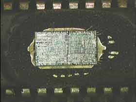
Break IC PIC16F616 Heximal
PIC16F610/16HV610 Register locations 40h-7Fh in Bank 0 are General Purpose Registers, implemented PC gram counter capable of addressing an 8k x 14 program memory space. Only the first 1K x 14 (0000h-3FF) for the PIC16F610/16HV610 and the first 2K x 14 (0000h-07FFh) for the PIC16F616/16HV616 is physically implemented to facilitate the process of Copy Microcontroller PIC16F737 Flash.
Accessing a location above these boundaries will cause a wraparound within the first 1K x 14 space (PIC16F610/16HV610) and 2K x 14 space (PIC16F616/16HV616). The Reset vector is at 0000h and the interrupt vector is at 0004h after Break IC PIC16F616 Heximal
Break IC PIC16F610 Binary
We can break IC PIC16F610 Binary, please view the Microchip IC PIC16F610 features for your reference:
High-Performance RISC CPU:
· Only 35 instructions to learn:
– All single-cycle instructions except branches
· Operating speed:
– DC – 20 MHz oscillator/clock input
– DC – 200 ns instruction cycle
· Interrupt capability
· 8-level deep hardware stack
· Direct, Indirect and Relative Addressing modes
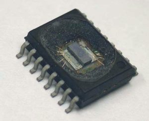
Break IC PIC16F610 Binary
Special Microcontroller Features:
· Precision Internal Oscillator:
– Factory calibrated to ±1%, typical
– User selectable frequency: 4 MHz or 8 MHz
· Power-Saving Sleep mode
· Voltage range:
– PIC16F610/616: 2.0V to 5.5V
– PIC16HV610/616: 2.0V to user defined maximum (see note)
· Industrial and Extended Temperature range
· Power-on Reset (POR)
· Power-up Timer (PWRT) and Oscillator Start-up Timer (OST)
· Brown-out Reset (BOR)
· Watchdog Timer (WDT) with independent oscillator for reliable operation only after the process of Attack MCU PIC12F675 Binary has been completed.
· Multiplexed Master Clear with pull-up/input pin
· Programmable code protection
· High Endurance Flash:
– 100,000 write Flash endurance
– Flash retention: > 40 years for the purpose of break IC PIC16F610 Binary
Low-Power Features:
· Standby Current:
– 50 nA @ 2.0V, typical
· Operating Current:
– 20 ìA @ 32 kHz, 2.0V, typical
– 220 ìA @ 4 MHz, 2.0V, typical
· Watchdog Timer Current:
– 1 ìA @ 2.0V, typical
Peripheral Features:
· Shunt Voltage Regulator (PIC16HV610/616 only):
– 5 volt regulation
– 4 mA to 50 mA shunt range
· 11 I/O pins and 1 input only
– High current source/sink for direct LED drive
– Interrupt-on-Change pins
– Individually programmable weak pull-ups
· Analog Comparator module with:
– Two analog comparators
– Programmable on-chip voltage reference (CVREF) module (% of VDD)
– Fixed Voltage Reference
– Comparator inputs and outputs externally accessible
– SR Latch
– Built-In Hysteresis (user selectable)
· Timer0: 8-bit timer/counter with 8-bit programmable prescaler
· Enhanced Timer1:
– 16-bit timer/counter with prescaler
– External Timer1 Gate (count enable)
– Option to use OSC1 and OSC2 in LP mode as Timer1 oscillator if INTOSC mode selected
– Timer1 oscillator
· In-Circuit Serial ProgrammingTM (ICSPTM) via two pins
Break IC PIC16F690 Code
The Program Counter (PC) is 13 bits wide. The low byte comes from the PCL register, which is a readable and writable register in order to Break IC PIC16F690 Code. The high byte (PC<12:8>) is not directly readable or writable and comes from PCLATH. On any Reset, the PC is cleared. Figure 2-9 shows the two situations for the loading of the PC.
The upper example in Figure 2-9 shows how the PC is loaded on a write to PCL (PCLATH<4:0> → PCH). The lower example in Figure 2-9 shows how the PC is loaded during aCALL or GOTO instruction (PCLATH<4:3> → PCH).
Executing any instruction with the PCL register as the destination simultaneously causes the Program Counter PC<12:8> bits (PCH) to be replaced by the contents of the PCLATH register.
This allows the entire contents of the program counter to be changed by writing the desired upper 5 bits to the PCLATH register to facilitate the process of Break IC PIC16C556A Software. When the lower 8 bits are written to the PCL register, all 13 bits of the program counter will change to the values contained in the PCLATH register and those being written to the PCL register.
ospace:none’>Figure 2-9 shows how the PC is loaded during aCALL or GOTO instruction (PCLATH<4:3> → PCH).
to the program counter (ADDWF PCL). Care should be exercised when jumping into a look-up table or program branch table (computed GOTO) by modifying the PCL register.

Break IC PIC16F690 Code
Assuming that PCLATH is set to the table start address, if the table length is greater than 255 instructions or if the lower 8 bits of the memory address rolls over from 0xFF to 0×00 in the middle of nd those being written to the PCL register. ospace:none’>Figure 2-9 shows how the PC is loaded during aCALL or GOTO instruction (PCLATH<4:3> → PCH).
the table, then PCLATH must be incremented for each address rollover that occurs between the table beginning and the target location within the table. For more information refer to Application Note AN556,
The INDF register is not a physical register. Addressing the INDF register will cause indirect addressing. Indirect addressing is possible by using the INDF register. Any instruction using the INDF register actually instruction (PCLATH<4:3> → PCH) can cause the problem on Copy Microcontroller PIC16CR83 Heximal.
accesses data pointed to by the File Select Register (FSR). Reading INDF itself indirectly will produce 00h. Writing to the INDF register indirectly results in a no operation (although Status bits may be affected). An effective 9-bit address is obtained by concatenating the 8-bit FSR and the IRP bit of the STATUS register before the MCU cracking has begun.
A simple program to clear RAM location 20h-2Fh using indirect addressing is shown in Example 2-1 address rolls over from 0xFF to 0×00 in the middle of nd those being written to the PCL register. ospace:none’>Figure 2-9 shows how the PC is loaded during aCALL or GOTO instruction (PCLATH<4:3> → PCH) for the purpose of Break IC PIC16F690 Code.
Break IC PIC16F689 Software
The data memory is partitioned into four banks which contain the General Purpose Registers (GPR) and the Special Function Registers (SFR). The Special Function Registers are located in the first 32 locations of each bank, in order to Break IC PIC16F689 Software, we need to figure out the location of special function register.
The General Purpose Registers, implemented as static RAM, are located in the last 96 locations of each Bank. Register locations F0h-FFh in Bank 1, 170h-17Fh in Bank 2 and 1F0h-1FFh in Bank 3 point to addresses 70h-7Fh in Bank 0.
The actual number of General Purpose Resisters (GPR) in each Bank depends on the device. Details are shown in Figures 2-4 through 2-8. All other RAM is unimplemented and returns ‘0’ when Reset Vector 0000h read. RP<1:0> of the STATUS register are the bank select bits.
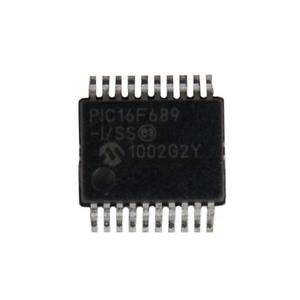
Break IC PIC16F689 Software
The register file is organized as 128 x 8 in the PIC16F687 and 256 x 8 in the PIC16F689. Each register is accessed, either directly or indirectly, through the File Select Register (FSR) (see Section 2.4 “Indirect Addressing, INDF and FSR Registers”). SPECIAL FUNCTION REGISTERS:
The Special Function Registers are registers used by the CPU and peripheral functions for controlling the desired operation of the device (see Tables 2-1 through 2-4). These registers are static RAM which are useful when Break Microcontroller PIC18F4220 Binary.
The special registers can be classified into two sets: core and peripheral. The Special Function Registers associated with the “core” are described in this section. Registers related to the operation of peripheral features are described in the section of that peripheral feature.
The STATUS register, shown in Register 2-1, contains:
· the arithmetic status of the ALU
· the Reset status
· the bank select bits for data memory (GPR and SFR)
The STATUS register can be the destination for any instruction, like any other register. If the STATUS register is the destination for an instruction that affects the Z, DC or C bits, then the write to these three bits is disabled. These bits are set or cleared according to the device logic to facilitate the process of Unlock Microcontroller. Furthermore, the TO and PD bits are not writable. Therefore, the result of an instruction with the STATUS register as destination may be different than intended for the purpose.
Break IC PIC16F687 Firmware
It is also very important to understand the peripheral features when Break IC PIC16F687 Firmware
Peripheral Features:
· 17 I/O pins and 1 input only pin:
– High current source/sink for direct LED drive
– Interrupt-on-Change pin
– Individually programmable weak pull-ups
– Ultra Low-Power Wake-up (ULPWU)
· Analog Comparator module with:
– Two analog comparators
– Programmable on-chip voltage reference (CVREF) module (% of VDD)
– Comparator inputs and outputs externally accessible which can be used for Copy MCU PIC16C72 Software
– SR Latch mode
– Timer 1 Gate Sync Latch
– Fixed 0.6V VREF
· A/D Converter:
– 10-bit resolution and 12 channels
· Timer0: 8-bit timer/counter with 8-bit programmable prescaler
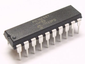
Break IC PIC16F687 Firmware
· Enhanced Timer1:
– 16-bit timer/counter with prescaler
– External Timer1 Gate (count enable)
– Option to use OSC1 and OSC2 in LP mode as Timer1 oscillator if INTOSC mode selected
· Timer2: 8-bit timer/counter with 8-bit period register, prescaler and postscaler
· Enhanced Capture, Compare, PWM+ module:
– 16-bit Capture, max resolution 12.5 ns
– Compare, max resolution 200 ns
– 10-bit PWM with 1, 2 or 4 output channels, programmable “dead time”, max frequency 20 kHz
– PWM output steering control which can be manipulated to Break MCU PIC16C717 Program
· Synchronous Serial Port (SSP):
– SPI mode (Master and Slave)
· I2C™ (Master/Slave modes):
– I2C™ address mask
· In-Circuit Serial ProgrammingTM (ICSPTM) via two pins for the purpose
Program Memory Organization
The PIC16F687 has a 13-bit program counter capable of addressing an 8K x 14 program memory space. Only the first 1K x 14 (0000h-03FFh) is physically implemented for the PIC16F631, the first 2K x 14 (0000h-07FFh) for the PIC16F687, and the first 4K x 14 (0000h-0FFFh) for the PIC16F687. Accessing a location above these
boundaries will cause a wraparound. The Reset vector is at 0000h and the interrupt vector is at 0004h.
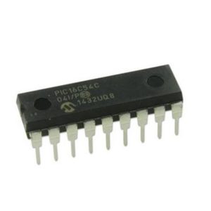
Break IC PIC16C54C Firmware
Break IC PIC16C54C Firmware from both eeprom and flash, needs to disable the security fuse bits:
12-bit wide instructions
8-bit wide data path
Seven or eight special function hardware registers
Two-level deep hardware stack
Direct, indirect and relative addressing modes for
data and instructions
Peripheral Features:
· 8-bit real time clock/counter (TMR0) with 8-bit programmable prescaler
· Power-on Reset (POR)
· Device Reset Timer (DRT)
(i.e., PIC16C54 refers to PIC16C54, PIC16C54A, and PIC16C54C), unless specifically called out otherwise for the purpose of break ic.
High-Performance RISC CPU:
· Only 33 single word instructions to learn
· All instructions are single cycle except for program branches which are two-cycle
· Operating speed: DC – 40 MHz clock input DC – 100 ns instruction cycle
Break IC PIC16C54C Firmware
· Watchdog Timer (WDT) with its own on-chip RC oscillator for reliable operation
· Programmable Code Protection
· Power saving SLEEP mode which can be used to Break IC PIC16F88 Data
· Selectable oscillator options:
– RC: Low cost RC oscillator
– XT: Standard crystal/resonator
– HS: High speed crystal/resonator
– LP: Power saving, low frequency crystal
CMOS Technology:
· Low power, high speed CMOS EPROM/ROM technology
· Fully static design
· Wide operating voltage and temperature range:
– EPROM Commercial/Industrial 2.0V to 6.25V
– ROM Commercial/Industrial 2.0V to 6.25V
– EPROM Extended 2.5V to 6.0V
– ROM Extended 2.5V to 6.0V
· Low power consumption
– < 2 mA typical @ 5V, 4 MHz
– 15 µA typical @ 3V, 32 kHz
– < 0.6 µA typical standby current
(with WDT disabled) @ 3V, 0°C to 70°C
Note:
In this document, figure and table titles refer to all varieties of the part number indicated, (i.e., The title “Figure 15-1: Load
Conditions For Device Timing Specifications – PIC16C54A”, also refers to PIC16LC54A and PIC16LV54A parts),
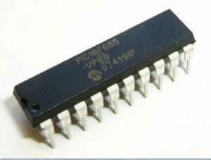
Break IC PIC16F685 Flash
Break IC PIC16F685 Flash needs to find out the location of this flash memory, so it is necessary to understand the structure of it:
Break IC PIC16F685 Flash
High-Performance RISC CPU:
· Only 35 instructions to learn:
– All single-cycle instructions except branches
· Operating speed:
– DC – 20 MHz oscillator/clock input
– DC – 200 ns instruction cycle
· Interrupt capability
· 8-level deep hardware stack
· Direct, Indirect and Relative Addressing modes
Special Microcontroller Features:
· Precision Internal Oscillator:
– Factory calibrated to ± 1%
– Software selectable frequency range of 8 MHz to 32 kHz
– Software tunable
– Two-Speed Start-up mode
– Crystal fail detect for critical applications and Break IC PIC16F873A Code
– Clock mode switching during operation for power savings
· Power-Saving Sleep mode
· Wide operating voltage range (2.0V-5.5V)
· Industrial and Extended Temperature range
· Power-on Reset (POR)
· Power-up Timer (PWRTE) and Oscillator Start-up Timer (OST)
· Brown-out Reset (BOR) with software control option
· Enhanced low-current Watchdog Timer (WDT) with on-chip oscillator (software selectable nominal 268 seconds with full prescaler) with software enable
· Multiplexed Master Clear/Input pin
· Programmable code protection to prevent the MCU Cracking
· High Endurance Flash/EEPROM cell:
– 100,000 write Flash endurance
– 1,000,000 write EEPROM endurance
– Flash/Data EEPROM retention: > 40 years
· Enhanced USART module:
– Supports RS-485, RS-232 and LIN 2.0
– Auto-Baud Detect
– Auto-wake-up on Start bit
Low-Power Features:
· Standby Current:
– 50 nA @ 2.0V, typical
· Operating Current:
– 11 ìA @ 32 kHz, 2.0V, typical
– 220 ìA @ 4 MHz, 2.0V, typical
· Watchdog Timer Current:
– <1 ìA @ 2.0V, typical for the purpose