Archive for the ‘Recover MCU’ Category
 Attack MCU PIC16F636 Binary
 October 15th, 2014 |
  Author:
 Attack MCU PIC16F636 Binary
Timer1 Operation in Asynchronous Counter Mode can greatly facilitate the process of Attack MCU PIC16F636 Binary.
If control bit T1SYNC (T1CON<2>) is set, the external clock input is not synchronized. The timer continues to increment asynchronous to the internal phase clocks. The timer will continue to run during SLEEP and can generate an interrupt on overflow, which will wake-up the processor. However, special precautions in software are needed to read/write the timer.
Timer1 Oscillator
A crystal oscillator circuit is built-in between pins OSC1 (input) and OSC2 (amplifier output). It is enabled by setting control bit T1OSCEN (T1CON<3>). The oscillator is a low power oscillator rated up to 32 kHz. It will continue to run during SLEEP. It is primarily intended for a 32 kHz crystal. Table 9-2 shows the capacitor selection for the Timer1 oscillator. The Timer1 oscillator is shared with the system LP oscillator. Thus, Timer1 can use this mode only when the system clock is derived from the internal oscillator.
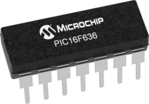
Attack MCU PIC16F636 Binary
Asynchronous Counter Mode.
As with the system LP oscillator, the user must provide a software time delay to ensure proper oscillator start-up.
TRISA5 and TRISA4 bits are set when the Timer1 oscillator is enabled. RA5 and RA4 read as ‘0’ and TRISA5 and TRISA4 bits read as ‘1’
The Timer1 oscillator is shared with the system LP oscillator. Thus, Timer1 can use this mode only when the system clock is derived from the internal oscillator.
Reading TMR1H or TMR1L, while the timer is running from an external asynchronous clock, will ensure a valid read (taken care of in hardware). However, the user should keep in mind that reading the 16-bit timer oscillator is enabled. RA5 and RA4 read as ‘0’ and TRISA5 and TRISA4 bits read as ‘1’ in two 8-bit values itself, poses certain problems, since the timer may overflow between the reads.
For writes, it is recommended that the user simply stop the timer and write the desired values. A write contention may occur by writing to the timer registers, while the register is incrementing. This may produce an unpredictable value in the timer register before CLONE IC.
Reading the 16-bit value requires some care. Examples 12-2 and 12-3 in the PICmicro™ Mid-Range MCU Family Reference Manual (DS33023) show how to read and write Timer1 when it is running in Asynchronous mode.
Attack MCU PIC16F676 Code
Attack MCU PIC16F676 Code
This document contains device specific information for the PIC16F676. Additional information may be found in the PICmicroTM Mid-Range Reference Manual (DS33023) from Attack MCU PIC16F676 Code, which may be obtained from your local Microchip Sales Representative or downloaded from the Microchip web site.
The Reference Manual should be considered a complementary document to this Data Sheet and is highly recommended reading for a better understanding of the device architecture and operation of the peripheral modules.
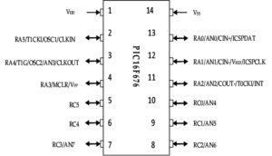
The PIC16F630 and PIC16F676 devices are covered by this Data Sheet. They are identical, except the PIC16F676 has a 10-bit A/D converter. They come in 14-pin PDIP, SOIC and TSSOP packages. Figure 1-1 shows a block diagram of the PIC16F630/676 devices. Table 1-1 shows the pinout description.
Attack MCU PIC16F676 Code
PROGRAM MEMORY ORGANIZATION
The PIC16F630/676 devices have a 13-bit program counter capable of addressing an 8K x 14 program memory space. Only the first 1K x 14 (0000h – 03FFh) for the PIC16F630/676 devices is physically implemented. Accessing a location above these boundaries will cause a wrap around within the first 1K x 14 space.
The RESET vector is at 0000h and the interrupt vector is at 0004h.
The data memory (see Figure 2-2) is partitioned into two banks, which contain the General Purpose registers and the Special Function registers. The Special Function registers are located in the first 32 locations of each bank. Register locations 20h-5Fh are General Purpose registers, implemented as static RAM and are mapped across both banks. All other RAM is unimplemented and returns ‘0’ when read. RP0 (STATUS<5>) is the bank select bit after CRACK MCU code.
SPECIAL FUNCTIONS REGISTERS
The Special Function registers are registers used by the CPU and peripheral functions for controlling the desired operation of the device (see Table 2-1). These registers are static RAM.
The special registers can be classified into two sets: core and peripheral. The Special Function registers associated with the “core” are described in this section. Those related to the operation of the peripheral features are described in the section of that peripheral feature.
Attack PIC MCU 16F506 Code
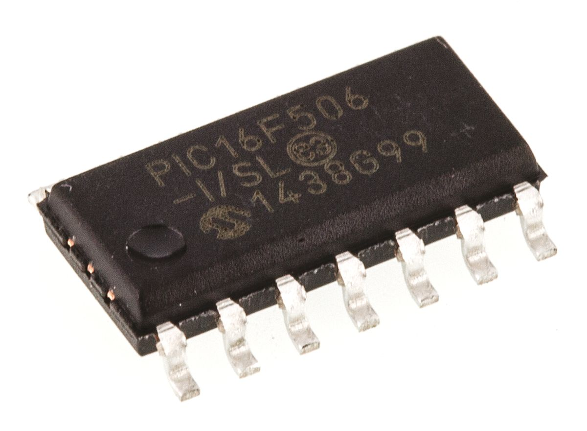
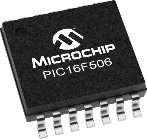
The PIC16F506 is a remarkably compact and efficient 14-pin MCU that has found its way into countless specialized applications since its inception. Known for its cost-effective Flash-based CMOS technology, this microcontroller is widely utilized in sectors ranging from basic consumer electronics and toy manufacturing to more sophisticated automotive climate controls and industrial timing relays. Its unique features, such as an internal 4MHz oscillator and a diverse set of I/O pins within a small footprint, make it an ideal candidate for embedded systems where space and power efficiency are paramount. However, most of these units are deployed with protective security bits enabled, creating a locked environment that safeguards the internal logic. For many organizations, the inability to access this secured program during a hardware failure or after losing the original development archive can lead to a complete operational standstill.
Our high-precision technical service offers a professional methodology to attack these hardware-level barriers and retrieve the critical binary data stored within the silicon. To successfully break the security of a protected MCU, our laboratory utilizes a specialized process to decapsulate the chip, exposing the internal memory structure for direct analysis. This allows our engineers to decode the heximal file directly from the flash or eeprom segments, effectively bypassing the encrypted or secured status of the device. Whether the objective is to clone a legacy controller to ensure production line continuity or to duplicate the firmware from a locked unit for essential maintenance, our service provides the most reliable way to hack the physical limitations of the chip. By transforming a protected binary back into a usable source code resource, we ensure that your embedded intelligence is never truly lost.
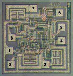
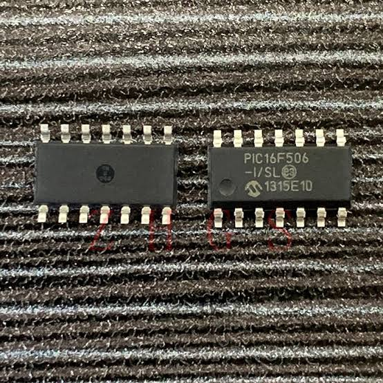
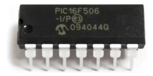
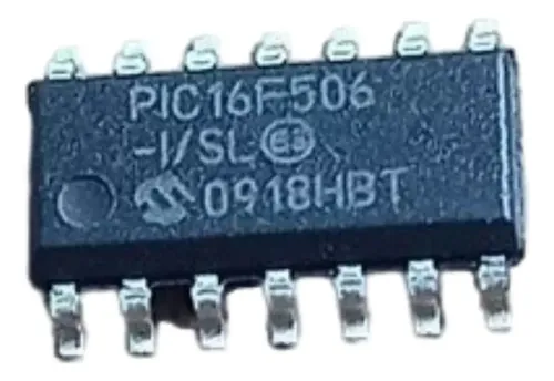
We can attack PIC MCU 16F506 Code, please view the PIC MCU features for your reference:
High-Performance RISC CPU:
· Only 33 single-word instructions to learn
· All single-cycle instructions except for program branches, which are two-cycle
· 12-bit wide instructions
· 2-level deep hardware stack
· Direct, Indirect and Relative Addressing modes for data and instructions
· 8-bit wide data path
· 10 Special Function Hardware registers (PIC12F510)
· 13 Special Function Hardware registers (PIC16F506)
· Operating speed:
– DC – 8 MHz Crystal Oscillator (PIC12F510)
– DC – 500 ns instruction cycle (PIC12F510)
– DC – 20 MHz Crystal Oscillator (PIC16F506)
– DC – 200 ns instruction cycle (PIC16F506)
Special Microcontroller Features:
· 4 or 8 MHz selectable precision internal oscillator:
– Factory calibrated to ±1% when attack PIC MCU
· In-Circuit Serial Programming™ (ICSP™)
· In-Circuit Debugging (ICD) support
· Power-on Reset (POR)
· Device Reset Timer (DRT):
– Short DRT (1.125 ms, typical) for INTOSC, EXTRC and EC
– DRT (18 ms, typical) for HS, XT and LP
· Watchdog Timer (WDT) with dedicated on-chip RC oscillator for reliable operation
· Programmable code protection
· Multiplexed MCLR input pin if attack PIC MCU
· Selectable internal weak pull-ups on I/O pins
· Power-Saving Sleep mode
· Wake-up from Sleep on pin change
· Wake-up from Sleep on comparator change
Selectable oscillator options:
– INTOSC: 4/8 MHz precision Internal oscillator
– EXTRC: External low-cost RC oscillator
– XT: Standard crystal/resonator
– LP: Power-saving, low-frequency crystal
– HS: High-speed crystal/resonator (PIC16F506 only)
– EC: High-speed external clock input (PIC16F506 only)
· Analog-to-Digital (A/D) Converter:
– 8-bit resolution
– 4-input channels (1 channel is dedicated to conversion of the internal 0.6V absolute voltage reference)
· High current sink/source for direct LED drive
· 8-bit real-time clock/counter (TMR0) with 8-bit programmable prescaler
Low-Power Features/CMOS Technology:
· Operating Current:
– < 170 ìA @ 2V, 4 MHz
· Standby Current:
– 100 nA @ 2V, typical
· Low-power, high-speed Flash technology:
– 100,000 cycle Flash endurance
– > 40-year retention
· Fully static design
· Wide operating voltage range: 2.0V to 5.5V
· Wide temperature range:
– Industrial: -40°C to +85°C
– Extended: -40°C to +125°C e:AR-SA’>programmable prescaler
The fundamental purpose of performing a targeted attack to break the security of a PIC16F506 is to protect the long-term viability of proprietary technology in an era of rapid obsolescence. For end users, the ability to retrieve a heximal archive from a locked MCU is often the only way to clone or duplicate vital system components when a supplier no longer exists. By choosing to decode or hack the secured architecture of an existing chip, you can successfully migrate your program data to new hardware without the massive expense of a ground-up redesign. Our expertise ensures that you can duplicate the flash and eeprom contents of any embedded controller, ensuring that your protected logic remains an accessible asset for your organization. This technical bridge allows for the seamless recovery of a binary file that would otherwise be permanently trapped within a secured silicon housing.
Ultimately, our recovery service provides the end user with an unparalleled level of hardware independence and peace of mind. Instead of struggling with the impossible task of recreating lost source code, you can simply retrieve the heximal program and clone the locked data directly onto a fresh MCU. We specialize in the precision required to decapsulate and attack these high-security chips, ensuring that every binary file is handled with surgical accuracy and total integrity. By providing a reliable way to decode and duplicate the firmware of a secured PIC16F506, we turn a protected archive into a living, functional part of your current technological ecosystem. Our commitment is to ensure that your data, memory, and program files remain within your control, regardless of the protective measures originally placed upon the embedded silicon.
Attack MCU PIC16C712 Binary
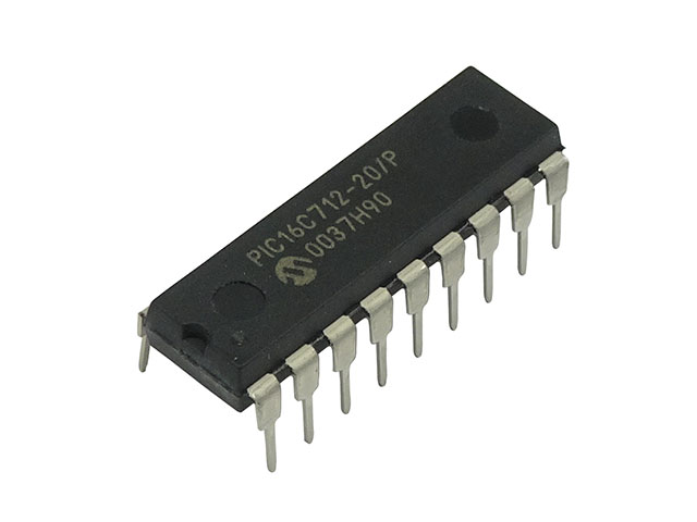
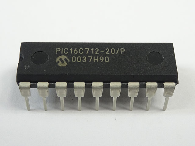
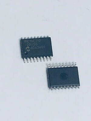
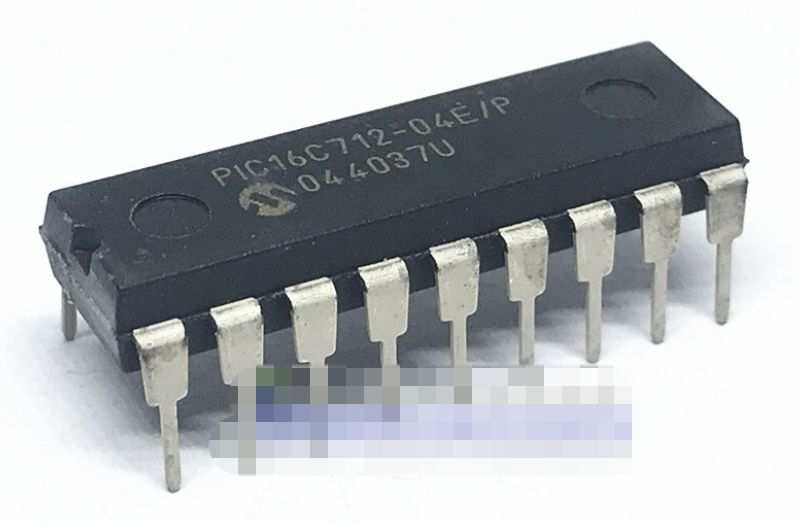
The PIC16C712 stands as a veteran of the 8-bit embedded world, specifically engineered for cost-sensitive applications that require high-speed performance and integrated analog capabilities. This MCU is widely utilized in sectors ranging from telecommunications and security systems to precise motor control and household appliances. Its unique features include a versatile capture/compare/PWM module and a high-performance RISC CPU, making it a reliable choice for managing complex data streams in real-time. Despite its age, many industrial machines still rely on this specific architecture to maintain operational stability. However, because these chips often utilize protective security bits to keep the internal firmware locked, organizations frequently face a crisis when hardware fails and the original source code or binary file is nowhere to be found.
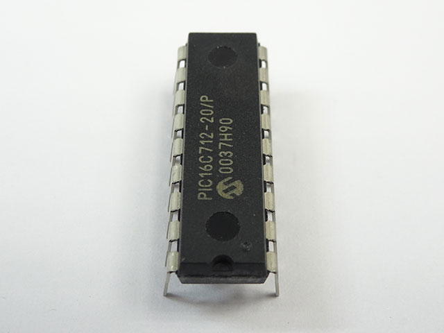
Our professional technical laboratory specializes in the ability to attack these hardware-level restrictions to retrieve the critical heximal data required for system restoration. To successfully break the security of a secured MCU, our engineers often perform a delicate procedure to decapsulate the integrated circuit, exposing the silicon die to specialized light or micro-probing equipment. This physical approach allows us to decode the protected logic gates and extract the binary archive directly from the memory cells. Whether the goal is to clone a legacy controller for a mission-critical backup or to duplicate the program from an encrypted chip to ensure future compatibility, our service provides a non-destructive pathway to hack the limitations of embedded silicon. By concentrating our expertise on the PIC16C712, we ensure that your locked flash or eeprom content is recovered with absolute precision, turning a secured component back into a viable source code asset.
We can Attack MCU PIC16C712 Binary, please view the MCU PIC16C712 features for your reference:
Microcontroller Core Features:
· High-performance RISC CPU
· Only 35 single word instructions to learn
· All single cycle instructions except for program branches which are two cycle when Attack MCU PIC16C712 Binary
· Operating speed: DC – 20 MHz clock input DC – 200 ns instruction cycle
· Interrupt capability (up to 7 internal/external interrupt sources)
· Eight level deep hardware stack
· Direct, indirect and relative addressing modes
· Power-on Reset (POR)
· Power-up Timer (PWRT) and Oscillator Start-up Timer (OST)
· Watchdog Timer (WDT) with its own on-chip RC oscillator for reliable operation
· Brown-out detection circuitry for Brown-out Reset (BOR)
· Programmable code-protection
· Power saving SLEEP mode
· Selectable oscillator options
· Low-power, high-speed CMOS EPROM technology
· Fully static design
· In-Circuit Serial Programming (ICSP) after Attack MCU PIC16C712 Binary
· Wide operating voltage range: 2.5V to 5.5V
· High Sink/Source Current 25/25 mA
· Commercial, Industrial and Extended temperature ranges
· Low-power consumption:
– < 2 mA @ 5V, 4 MHz
– 22.5 µA typical @ 3V, 32 kHz
– < 1 µA typical standby current
Peripheral Features:
· Timer0: 8-bit timer/counter with 8-bit prescaler
· Timer1: 16-bit timer/counter with prescaler can be incremented during sleep via external crystal/clock
· Timer2: 8-bit timer/counter with 8-bit period register, prescaler and postscaler
· Capture, Compare, PWM module
· Capture is 16-bit, max. resolution is 12.5 ns, Compare is 16-bit, max. resolution is 200 ns, PWM maximum resolution is 10-bit
· 8-bit multi-channel Analog-to-Digital converter
This document contains device-specific information. Additional information may be found in the PICmicro™ Mid-Range Reference Manual, (DS33023), which may be obtained from your local Microchip Sales Representative or downloaded from the Microchip website when Attack MCU. The Reference Manual should be considered a complementary document to this data sheet, and is highly recommended reading for a better understanding of the device architecture and operation of the peripheral modules before Attack MCU PIC16C712 Binary.
The underlying purpose of such a targeted attack is rarely about compromise, but rather about the survival of essential technology. For many end users, the ability to retrieve a heximal archive from a protected MCU is a mechanical necessity that saves thousands of dollars in redevelopment costs. By choosing to decode or hack the secured architecture of an aging PIC16C712, manufacturers can clone or duplicate the firmware to fresh hardware, effectively extending the lifecycle of their equipment. Our service serves as a vital bridge, allowing you to duplicate the flash and eeprom data that was previously trapped within a locked or encrypted environment. This ensures that the binary program remains functional, even when the original supplier is no longer available to provide support or replacement parts.
Ultimately, our recovery service provides the end user with the confidence that their embedded infrastructure is never truly lost. Instead of facing the impossibility of rewriting decades-old source code, you can retrieve the heximal file and clone the locked program directly onto a compatible MCU. We specialize in the precision required to decapsulate and attack these high-security chips, ensuring that the binary data is handled with the highest level of integrity. By providing a reliable way to decode and duplicate the firmware of a secured PIC16C712, we turn a protected archive into a living part of your current operations. Our commitment is to ensure that your data, memory, and program files remain accessible, regardless of the protective measures originally placed upon the silicon.
Attack MCU PIC16C715 Software
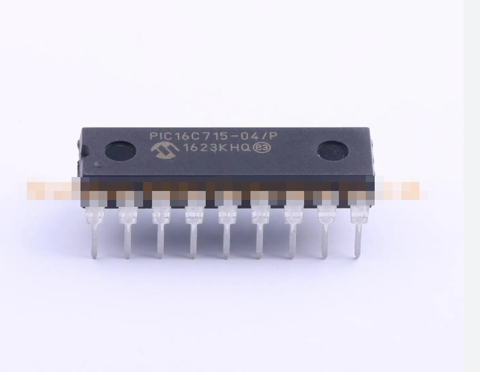
The PIC16C715 is a classic 8‑bit microcontroller from Microchip’s mid‑range family, built around embedded EPROM technology. Unlike modern flash devices, this chip is one‑time programmable (OTP) – meaning its memory can be written exactly once. It features 3.5KB of program memory, 128 bytes of EEPROM‑like data storage, and a built‑in 4‑channel 8‑bit ADC. Due to its high reliability and low cost, the PIC16C715 was widely deployed in automotive keyless entry systems, industrial sensor interfaces, medical infusion pumps, and consumer appliance controllers. Many manufacturers set protective lock bits to secure the binary file inside, turning the microcontroller into a locked black box. When the original source code is lost or the device becomes obsolete, the only archive of the firmware remains trapped in the protected memory. Recovering that data is critical to avoid scrapping expensive equipment.
PORTB is an 8-bit wide bi-directional port. The corresponding data direction register is TRISB. Setting a bit in the TRISB register puts the corresponding output driver in a hi-impedance input mode when Attack MCU PIC16C715 Software. Clearing a bit in the TRISB register puts the contents of the output latch on the selected pin(s).
Each of the PORTB pins has a weak internal pull-up. A single control bit can turn on all the pull-ups. This is performed by clearing bit RBPU (OPTION<7>). The weak pull-up is automatically turned off when the port pin is configured as an output. The pull-ups are disabled on a Power-on Reset.
Four of PORTB’s pins, RB7:RB4, have an interrupt on change feature. Only pins configured as inputs can cause this interrupt to occur (i.e. any RB7:RB4 pin configured as an output is excluded from the interrupt on change comparison).
To attack a locked PIC16C715, standard programmers are useless because the protective encrypted lock bits completely block any readout of the program memory. Our service employs specialised invasive techniques tailored for OTP chips. First, we decapsulate the plastic package using precise chemical etching to expose the silicon die. Then, we hack into the memory array by probing the data buses or exploiting the EPROM cell characteristics. The goal is to decode the binary program – a heximal file that represents the original source code logic. Once we retrieve the firmware, we can clone or duplicate it into a fresh microcontroller (such as a compatible flash‑based PIC or an exact OTP replacement). This break process is non‑destructive to the data itself, preserving the archive integrity. Unlike flash chips, OTP devices like the PIC16C715 require careful handling because the memory cannot be erased or rewritten, making our decapsulate and retrieve method the only viable solution.
The input pins (of RB7:RB4) are compared with the old value latched on the last attack of PORTB. The “mismatch” outputs of RB7:RB4 are OR’ed together to generate the RB Port Change Interrupt with flag bit RBIF (INTCON<0>).
Any instruction which writes, operates internally as a attack followed by a write operation. The BCF and BSF instructions, for example, attack the register into the CPU, execute the bit operation and write the result back to the register to ease the process of Attack MCU PIC16C715 Software. Caution must be used when these instructions are applied to a port with both inputs and outputs defined.
For example, a BSF operation on bit5 of PORTB will cause all eight bits of PORTB to be attack into the CPU. Then the BSF operation takes place on bit5 and PORTB is written to the output latches.
If another bit of PORTB is used as a bi-directional I/O pin (e.g., bit0) and it is defined as an input at this time, the input signal present on the pin itself would be attack into the CPU and rewritten to the data latch of this particular pin, overwriting the previous content. As long as the pin stays in the input mode, no problem occurs. However, if bit0 is switched to an output, the content of the data latch may now be unknown.
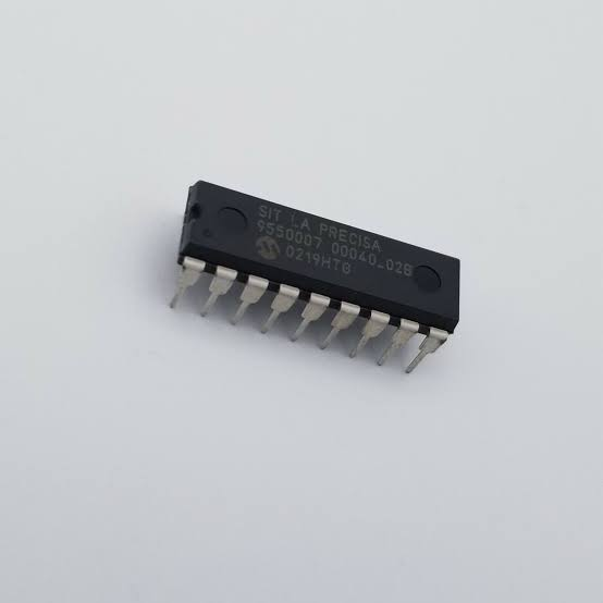
The demand to attack and recover firmware from secured PIC16C715 microcontrollers comes from urgent industrial needs. First, obsolete automation lines: many factory sensors and controllers still run on this chip, but the original heximal file was lost when a supplier closed. Second, medical device maintenance: infusion pumps and diagnostic tools using the PIC16C715 cannot be cloned without decoding the locked program. Third, automotive electronics: keyless entry modules with protected memory fail over time, and manufacturers no longer provide replacement chips. By performing a clean retrieve and duplicate of the binary archive, we enable clients to clone the firmware into new microcontrollers – avoiding costly system redesigns. The benefits are tangible: extended product lifecycle, reduced e‑waste, and preserved intellectual property without needing the original source code.
The actual write to an I/O port happens at the end of an instruction cycle, whereas for attacking, the data must be valid at the beginning of the instruction cycle. Therefore, care must be exercised if a write followed by a attack operation is carried out on the same I/O port. The sequence of instructions should be such to allow the pin voltage to stabilize (load dependent) before the next instruction which causes that file to be attack into the CPU is executed. Otherwise, the previous state of that pin may be attack into the CPU rather than the new state. When in doubt, it is better to separate these instructions with a NOP or another instruction not accessing this I/O port.
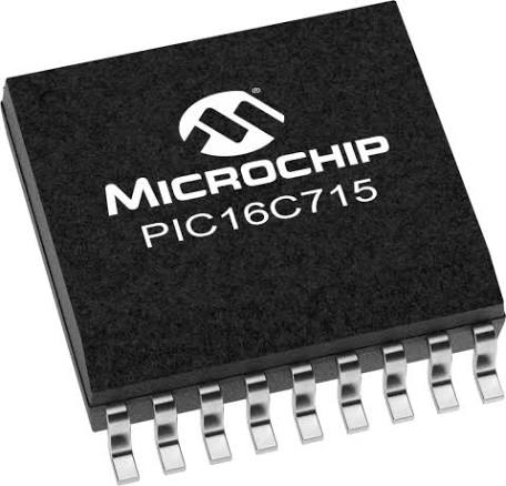
We offer confidential, fast, and precise attack services for the PIC16C715 and many other OTP microcontrollers. Every break procedure is performed with care to preserve data integrity. Contact us with your locked chip, and we will decapsulate, decode, and retrieve the complete binary or heximal file – turning a protective memory into a usable archive for production, cloning, or reverse engineering.
Attack Chip PIC16C73A Program
The Synchronous Serial Port can be configured as either a 3-wire Serial Peripheral Interface (SPI) or the two-wire Inter-Integrated Circuit (I2C) bus which can be used to Attack Chip PIC16C73A Program.
The Universal Synchronous Asynchronous Receiver Transmitter (USART) is also known as the Serial Communications Interface or SCI. Also a 5-channel high-speed 8-bit A/D is provided.The 8-bit resolution is ideally suited for applications requiring low-cost analog interface, e.g. thermostat control, pressure sensing, etc.
The PIC16C73A devices have 192 bytes of RAM, while the PIC16C73A has 368 bytes of RAM. Each device has 33 I/O pins. In addition several peripheral features are available including: three timer/counters, two Capture/Compare/PWM modules and two serial ports.
The Synchronous Serial Port can be configured as either a 3-wire Serial Peripheral Interface (SPI) or the two-wire Inter-Integrated Circuit (I2C) bus. The Universal Synchronous Asynchronous Receiver Transmitter (USART) is also known as the Serial Communications Interface or SCI.
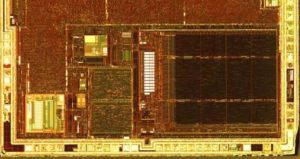
Attack Chip PIC16C73A Program
An 8-bit Parallel Slave Port is provided. Also an 8-channel high-speed 8-bit A/D is provided. The 8-bit resolution is ideally suited for applications requiring low-cost analog interface, e.g. thermostat control, pressure sensing, etc.
The PIC16C7X family has special features to reduce external components, thus reducing cost, enhancing system reliability and reducing power consumption.
There are four oscillator options, of which the single pin RC oscillator provides a low-cost solution, the LP oscillator minimizes power consumption, XT is a standard crystal, and the HS is for High Speed crystals. The SLEEP (power-down) feature provides a power saving mode. The user can wake up the chip from SLEEP through several external and internal interrupts and resets to Attack Chip PIC16C73A Program.
A highly reliable Watchdog Timer with its own on-chip RC oscillator provides protection against software lock-up. A UV erasable CERDIP packaged version is ideal for code development while the cost-effective One-Time-Programmable (OTP) version is suitable for production in any volume.
The PIC16C7X family fits perfectly in applications ranging from security and remote sensors to appliance control and automotive. The EPROM technology makes customization of application programs (transmitter codes, motor speeds, receiver frequencies, etc.) extremely fast and convenient.
The small footprint packages make this microcontroller series perfect for all applications with space limitations when Attack Chip. Low cost, low power, high performance, ease of use and I/O flexibility make the PIC16C7X very versatile even in areas where no microcontroller use has been considered before (e.g. timer functions, serial communication, capture and compare, PWM functions and coprocessor applications).
Attack IC PIC16C74B Binary
Depending on application and production requirements, the proper device option can be selected using the information in the PIC16C74B Product Identification System section at the end of this data sheet which can help to ease the process of Attack IC PIC16C74B Binary.
For the PIC16C7X family, there are two device “types” as indicated in the device number:
1. C, as in PIC16C74. These devices have EPROM type memory and operate over the standard voltage range.
2. LC, as in PIC16LC74. These devices have EPROM type memory and operate over an extended voltage range.
The UV erasable version, offered in windowed CERDIP packages, is optimal for prototype development and pilot programs. This version can be erased and reprogrammed to any of the oscillator modes. The availability of OTP devices is especially useful for customers who need the flexibility for frequent code updates and small volume applications.
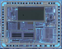
Attack IC PIC16C74B Binary
The OTP devices, packaged in plastic packages, permit the user to program them once. In addition to the program memory, the configuration bits must also be programmed.
Microchip offers a QTP Programming Service for factory production orders. This service is made available for users who choose not to program a medium to high quantity of units and whose code patterns have stabilized to prohibit the operation of Attack IC PIC16C74B Binary. The devices are identical to the OTP devices but with all EPROM locations and configuration options already programmed by the factory.
The high performance of the PIC16CXX family can be attributed to a number of architectural features commonly found in RISC microprocessors. To begin with, the PIC16CXX uses a Harvard architecture, in which program and data are accessed from separate memories using separate buses.
This improves bandwidth over traditional von Neumann architecture, in which program and data are fetched from the same memory using the same bus. Separating program and data buses further allows instructions to be sized differently than the 8-bit wide data word. Instruction opcodes are 14-bits wide, making it possible to have all single word instructions. A 14-bit wide program memory access bus fetches a 14-bit instruction in a single cycle.
A two-stage pipeline overlaps fetch and execution of instructions (Example 3-1). Consequently, most instructions execute in a single cycle (200 ns @ 20 MHz) except for program branches. All devices covered by this data sheet contain 4K x 14-bit program memory and 192 x 8-bit data memory.
Attack CPLD EPM7096QC100-10 Binary
We can Attack CPLD EPM7096QC100-10 Binary, please view CPLD EPM7096QC100-10 features for your reference:
High-performance, EEPROM-based programmable logic devices (PLDs) based on second-generation MAX® architecture 5.0-V in-system programmability (ISP) through the built-in IEEE Std. 1149.1 Joint Test Action Group (JTAG) interface available in MAX 7000S devices
– ISP circuitry compatible with IEEE Std. 1532
Includes 5.0-V MAX 7000 devices and 5.0-V ISP-based MAX 7000S devices
Built-in JTAG boundary-scan test (BST) circuitry in MAX 7000S devices with 128 or more macrocells
Complete EPLD family with logic densities ranging from 600 to 5,000 usable gates (see Tables 1 and 2) 5-ns pin-to-pin logic delays with up to 175.4-MHz counter frequencies (including interconnect) PCI-compliant devices available.
Open-drain output option in MAX 7000S devices
Programmable macrocell flipflops with individual clear, preset, clock, and clock enable controls
Programmable power-saving mode for a reduction of over 50% in each macrocell.
Configurable expander product-term distribution, allowing up to 32 product terms per macrocell 44 to 208 pins available in plastic J-lead chip carrier (PLCC), ceramic pin-grid array (PGA), plastic quad flat pack (PQFP), power quad flat pack (RQFP), and 1.0-mm thin quad flat pack (TQFP) packages.
Programmable security bit for protection of proprietary designs
– MultiVoltTM I/O interface operation, allowing devices to interface with 3.3-V or 5.0-V devices (MultiVolt I/O operation is not available in 44-pin packages) – Pin compatible with low-voltage MAX 7000A and MAX 7000B devices.
Enhanced features available in MAX 7000E and MAX 7000S devices
– Six pin- or logic-driven output enable signals
– Two global clock signals with optional inversion
– Enhanced interconnect resources for improved routability
– Fast input setup times provided by a dedicated path from I/O pin to macrocell registers
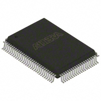
Attack CPLD EPM7096QC100-10 Binary
– Programmable output slew-rate control
Software design support and automatic place-and-route provided by
Altera’s development system for Windows-based PCs and Sun SPARCstation, and HP 9000 Series 700/800 workstations
Additional design entry and simulation support provided by EDIF 2 0 0 and 3 0 0 netlist files, library of parameterized modules (LPM), Verilog HDL, VHDL, and other interfaces to popular EDA tools from manufacturers such as Cadence, Exemplar Logic, Mentor Graphics, OrCAD, Synopsys, and VeriBest Programming support.
– Altera’s Master Programming Unit (MPU) and programming hardware from third-party manufacturers program all MAX 7000 devices
– The BitBlasterTM serial download cable, ByteBlasterMVTM parallel port download cable, and MasterBlasterTM serial/universal serial bus (USB) download cable program MAX 7000S devices.
 Posted in Recover MCU |
  Tags: ανακτώ ic eeprom, ανακτώ mcu archive, ανακτώ μικροελεγκτές firmware, ανακτώ ολοκληρωμένο κύκλωμα code, ανακτώ τσιπ program, αντιγράφω ic hex, αντιγράφω mcu bin, αντιγράφω μικροελεγκτές eeprom, αντιγράφω ολοκληρωμένο κύκλωμα software, αντιγράφω τσιπ flash |
  Comments Closed
Attack PLD EPM7128ELC84-10 Binary
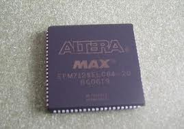
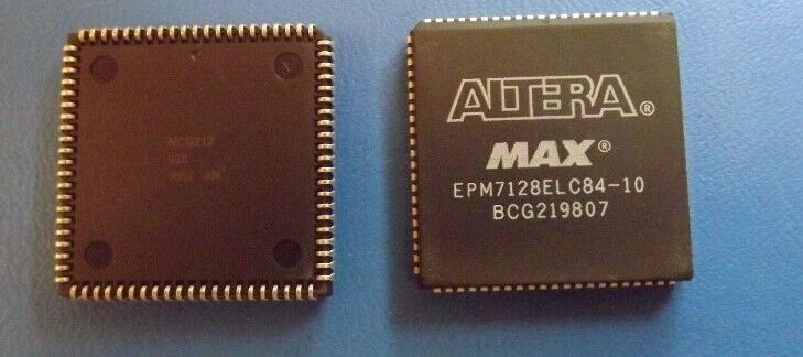
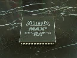
The EPM7128ELC84-10 is a high-density CPLD widely deployed in complex digital logic systems where deterministic timing, fast response, and stable embedded behavior are critical. It is commonly found in industrial automation platforms, telecom switching equipment, automotive control units, aerospace subsystems, and advanced instrumentation. As a programmable logic device, it stores configuration data that defines hardware-level logic behavior rather than executing traditional firmware instructions. This configuration, typically represented in binary or heximal form, acts as the functional equivalent of a program. However, when the original design archive, configuration file, or source code is lost, maintaining or replicating system functionality becomes extremely challenging. The Attack PLD EPM7128ELC84-10 Binary service is developed to help authorized users recover this critical embedded logic information from secured devices.
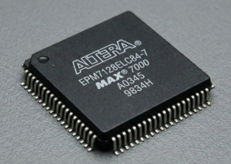
In real-world applications, the EPM7128ELC84-10 is often configured with protective, protected, locked, or encrypted mechanisms that restrict access to its internal memory and configuration data. These security measures prevent direct readout of the PLD’s binary or heximal program file, even for legitimate engineering purposes. Our service focuses on controlled methods to attack, break, or carefully decode these restrictions, allowing the safe retrieve of embedded configuration data. Through in-depth structural analysis of the PLD, we reconstruct the internal program, extract usable binary images, and rebuild complete archive outputs from secured devices. In advanced scenarios, specialized decapsulate approaches may be applied to expose deeply embedded memory structures, enabling access to otherwise inaccessible configuration elements. This process ensures that recovered data maintains fidelity to the original programmed logic.
Includes 5.0-V MAX 7000 devices and 5.0-V ISP-based MAX 7000S devices
Built-in JTAG boundary-scan test (BST) circuitry in MAX 7000S devices with 128 or more macrocells
Complete EPLD family with logic densities ranging from 600 to 5,000 usable gates (see Tables 1 and 2) 5-ns pin-to-pin logic delays with up to 175.4-MHz counter frequencies (including interconnect)
PCI-compliant devices available
Open-drain output option in MAX 7000S devices
Programmable macrocell flipflops with individual clear, preset, clock, and clock enable controls
Programmable power-saving mode for a reduction of over 50% in each macrocell
Configurable expander product-term distribution, allowing up to 32 product terms per macrocell
44 to 208 pins available in plastic J-lead chip carrier (PLCC), ceramic pin-grid array (PGA), plastic quad flat pack (PQFP), power quad flat pack (RQFP), and 1.0-mm thin quad flat pack (TQFP) packages.
Programmable security bit for protection of proprietary designs
3.3-V or 5.0-V operation
– MultiVoltTM I/O interface operation, allowing devices to interface with 3.3-V or 5.0-V devices after Attack PLD EPM7128ELC84-10 Binary (MultiVolt I/O operation is not available in 44-pin packages)
– Pin compatible with low-voltage MAX 7000A and MAX 7000B devices
Enhanced features available in MAX 7000E and MAX 7000S devices
– Six pin- or logic-driven output enable signals
– Two global clock signals with optional inversion
– Enhanced interconnect resources for improved routability
– Fast input setup times provided by a dedicated path from I/O pin to macrocell registers
– Programmable output slew-rate control
Software design support and automatic place-and-route provided by Altera’s development system for Windows-based PCs and Sun SPARCstation, and HP 9000 Series 700/800 workstations.
Additional design entry and simulation support provided by EDIF 2 0 0 and 3 0 0 netlist files, library of parameterized modules (LPM), Verilog HDL, VHDL, and other interfaces to popular EDA tools from manufacturers such as Cadence, Exemplar Logic, Mentor Graphics, OrCAD, Synopsys, and VeriBest.
Programming support
– Altera’s Master Programming Unit (MPU) and programming hardware from third-party manufacturers program all MAX 7000 devices
– The BitBlasterTM serial download cable, ByteBlasterMVTM parallel port download cable, and MasterBlasterTM serial/universal serial bus (USB) download cable program MAX 7000S devices
After extraction, the retrieved binary and heximal data must be translated into a usable engineering format. The recovered configuration is decoded and mapped into logical representations that reflect the original design intent. Although PLDs do not contain firmware in the conventional sense, their programmed logic functions as an embedded program, making accurate reconstruction essential. With properly processed file outputs and reconstructed source code equivalents, clients can clone or duplicate the original functionality onto replacement devices or migrate the design into newer CPLD or FPGA platforms. This allows legacy systems to continue operating without requiring a complete redesign from the ground up.
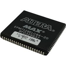
For equipment manufacturers, maintenance teams, and system integrators, the Attack PLD EPM7128ELC84-10 Binary service delivers substantial value. It enables recovery of critical configuration data, preservation of proven embedded logic, and extension of system lifecycle without disruption. Instead of replacing hardware due to locked or secured programmable devices, organizations can regain access to their essential design archive and embedded resources. By combining deep expertise in programmable logic with disciplined handling of protected and encrypted environments, this service provides a reliable pathway to restore, reuse, and replicate complex digital systems across a wide range of industries.
Attack AVR ATmega64L Program
Attack AVR ATmega64L Program is a professional embedded firmware recovery service developed for authorized projects that require access to critical program assets stored inside secured microcontrollers. The ATmega64L is a low-power AVR device widely deployed in industrial automation, portable instruments, access control systems, smart energy devices, and communication modules. Its efficient architecture, integrated flash and EEPROM memory, and stable embedded performance make it ideal for long-life applications. However, when original source code, firmware archives, or development documentation are lost, organizations often face serious operational risks that require controlled technical intervention.
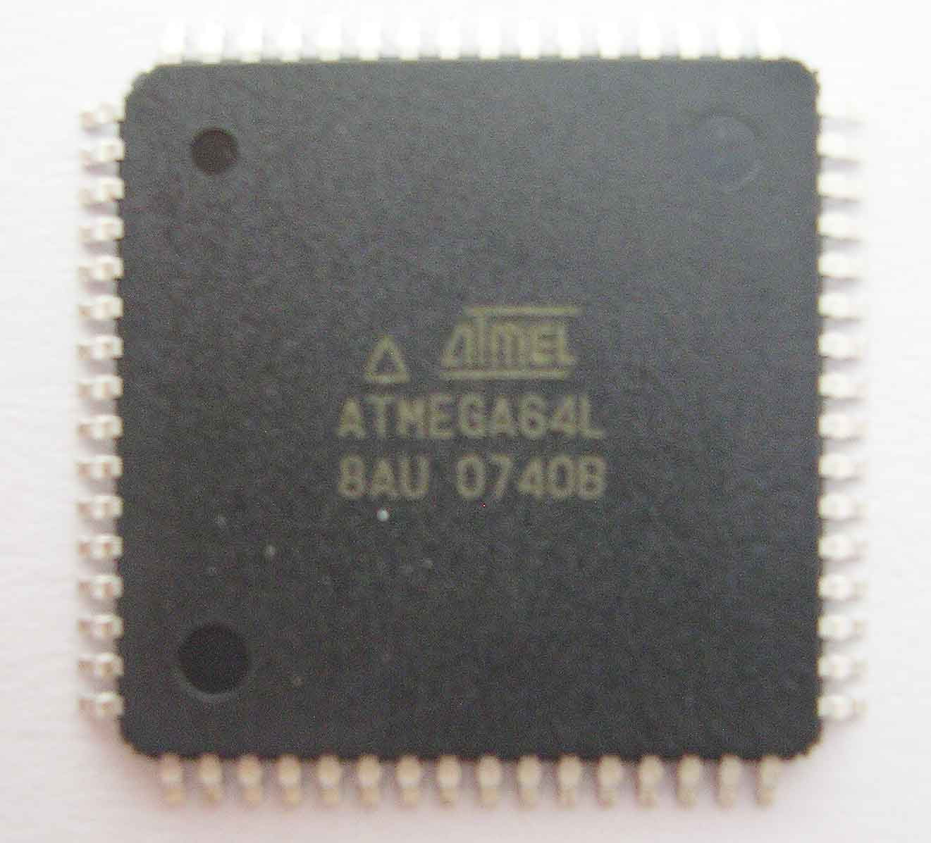
In many fielded products, the ATmega64L is configured with protective, protected, locked, or encrypted security mechanisms to secure firmware, binary, and heximal content stored in flash and EEPROM memory. Our Attack AVR ATmega64L Program service focuses on helping authorized clients attack and break these protection layers within a disciplined engineering framework. Through structured analysis, we work to decode secured memory regions, retrieve embedded firmware data, and reconstruct complete program files when official archives are no longer available. Whether the objective is to extract a binary image, recover a heximal file, or rebuild partial source code equivalents, the process centers on safely accessing flash memory and embedded data without compromising integrity. In advanced scenarios, controlled decapsulation concepts may be considered to reach deeply secured memory structures, always under strict handling procedures.
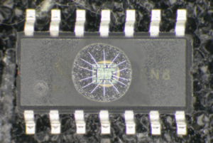
We can Attack AVR ATmega64L Program, please view below AVR ATMEGA64L features for your reference:
High-performance, Low-power Atmel® AVR® 8-bit Microcontroller
· Advanced RISC Architecture
– 130 Powerful Instructions – Most Single Clock Cycle Execution
– 32 x 8 General Purpose Working Registers + Peripheral Control Registers
– Fully Static Operation
– Up to 16 MIPS Throughput at 16 MHz
– On-chip 2-cycle Multiplier
High Endurance Non-volatile Memory segments
– 64 Kbytes of In-System Reprogrammable Flash program memory
– 2 Kbytes EEPROM
– 4 Kbytes Internal SRAM
– Write/Erase Cycles: 10,000 Flash/100,000 EEPROM
– Data retention: 20 years at 85°C/100 years at 25°C(1)
– Optional Boot Code Section with Independent Lock Bits
In-System Programming by On-chip Boot Program
True Read-While-Write Operation
– Up to 64 Kbytes Optional External Memory Space
– Programming Lock for Software Security
– SPI Interface for In-System Programming
JTAG (IEEE std. 1149.1 Compliant) Interface
– Boundary-scan Capabilities According to the JTAG Standard
– Extensive On-chip Debug Support
– Programming of Flash, EEPROM, Fuses, and Lock Bits through the JTAG Interface
Peripheral Features
– Two 8-bit Timer/Counters with Separate Prescalers and Compare Modes
– Two Expanded 16-bit Timer/Counters with Separate Prescaler, Compare Mode, and Capture Mode
– Real Time Counter with Separate Oscillator
– Two 8-bit PWM Channels
– 6 PWM Channels with Programmable Resolution from 1 to 16 Bits
– 8-channel, 10-bit ADC
8 Single-ended Channels
7 Differential Channels
2 Differential Channels with Programmable Gain (1x, 10x, 200x)
– Byte-oriented Two-wire Serial Interface
– Dual Programmable Serial USARTs
– Master/Slave SPI Serial Interface
– Programmable Watchdog Timer with On-chip Oscillator before Attack AVR
– On-chip Analog Comparator
Special Microcontroller Features
– Power-on Reset and Programmable Brown-out Detection
– Internal Calibrated RC Oscillator
– External and Internal Interrupt Sources
– Six Sleep Modes: Idle, ADC Noise Reduction, Power-save, Power-down, Standby and Extended Standby
– Software Selectable Clock Frequency
– ATmega103 Compatibility Mode Selected by a Fuse
– Global Pull-up Disable
I/O and Packages
– 53 Programmable I/O Lines
– 64-lead TQFP and 64-pad QFN/MLF
Operating Voltages
– 2.7V – 5.5V for ATmega64L
– 4.5V – 5.5V for ATmega64
Speed Grades
– 0 – 8 MHz for ATmega64L
– 0 – 16 MHz for ATmega64
Once firmware and memory data are retrieved, the next stage involves validation and preparation for practical use. Raw binary dumps must be decoded, organized into consistent program archives, and verified against expected memory layouts. This allows clients to clone or duplicate embedded functionality onto replacement devices, ensuring compatibility with existing hardware. By recovering secured firmware, EEPROM configuration data, and program files, we enable companies to maintain production continuity, support legacy systems, and migrate designs to updated platforms without rewriting complex embedded logic from the ground up.
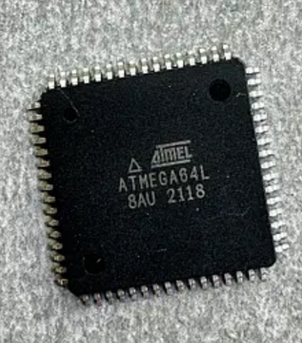
The benefits of the Attack AVR ATmega64L Program service extend beyond simple duplication. Clients gain long-term control over their embedded firmware assets, reduce downtime in critical industrial environments, and protect prior engineering investments. Instead of redesigning entire systems due to locked or encrypted memory, organizations can retrieve and preserve valuable embedded knowledge contained within the device. By combining AVR architecture expertise with careful handling of secured flash and memory environments, we provide a discreet, reliable solution for businesses that depend on stable, protected microcontroller platforms and require a responsible path to recover essential firmware and program data.