Archive for the ‘Recover MCU’ Category
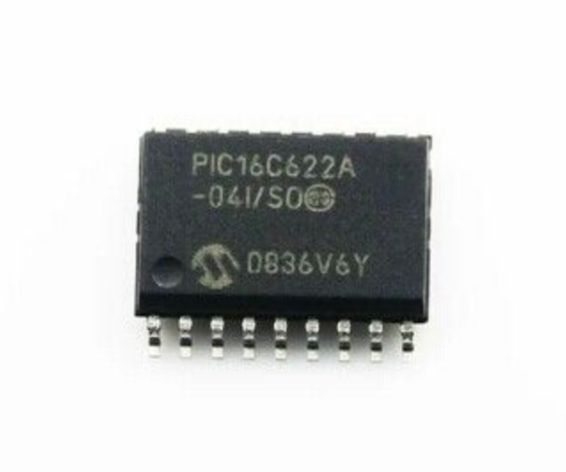
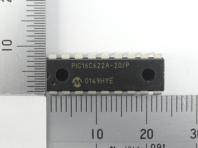
 Attack Chip PIC16C622A Software
 July 4th, 2014 |
  Author:
 The Microchip PIC16C622A remains a widely deployed 8-bit MCU across consumer electronics, industrial automation, automotive interfaces, security devices, sensor modules, and legacy embedded systems. Its reliability, compact architecture, and stable flash and eeprom handling make it a long-lasting favorite among engineers. However, once development archives or source code are lost, the internal software becomes extremely difficult to access—especially when the chip is in a protected, encrypted, or fully locked configuration. Our specialized service under the topic Attack Chip PIC16C622A Software is designed to help legitimate product owners safely retrieve, clone, or duplicate the MCU’s original firmware, without revealing or disclosing any sensitive technical methods.
Industrial Importance of the PIC16C622A
The PIC16C622A delivers a balance of low cost, low power usage, and versatile I/O features. This makes it a common choice in:
- Portable electronic products
- Access control, authentication, and smart security hardware
- Motor controllers and instrumentation devices
- Home appliances and small embedded consumer systems
- Customized OEM modules with long production cycles
In many of these applications, the internal binary, heximal, and configuration memory contain unique logic, calibration routines, and tailored program structures essential for stable system performance.
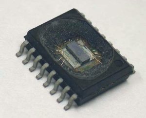
The high performance of the PIC16C62X family can be attributed to a number of architectural features commonly found in RISC microprocessors which is critical feature for Attack Chip PIC16C622A Software. To begin with, the PIC16C62X uses a Harvard architecture, in which, program and data are accessed from separate memories using separate busses. This improves bandwidth over traditional von Neumann architecture where program and data are fetched from the same memory. Separating program and data memory further allows instructions to be sized differently than 8-bit wide data word. Instruction opcodes are 14-bits wide making it possible to have all single word instructions.
A 14-bit wide program memory access bus fetches a 14-bit instruction in a single cycle. A two-stage pipeline overlaps fetch and execution of instructions.
Consequently, all instructions (35) execute in a single-cycle (200 ns @ 20 MHz) except for program branches. The PIC16C620A and PIC16CR620A address 512 x 14 on-chip program memory. The PIC16C621(A) addresses 1K x 14 program memory. The PIC16C622(A) addresses 2K x 14 program memory. All program memory is internal.
The PIC16C62X can directly or indirectly address its register files or data memory. All special function registers including the program counter are mapped in the data memory. The PIC16C62X have an orthogonal (symmetrical) instruction set that makes it possible to carry out any operation on any register using any addressing mode in order to Attack Chip PIC16C622A Software. This symmetrical nature and lack of ‘special optimal situations’ make programming with the PIC16C62X simple yet efficient. In addition, the learning curve is reduced significantly.
The PIC16C62X devices contain an 8-bit ALU and working register. The ALU is a general purpose arithmetic unit. It performs arithmetic and Boolean functions between data in the working register and any register file.
The ALU is 8-bit wide and capable of addition, subtraction, shift and logical operations. Unless otherwise mentioned, arithmetic operations are two’s complement in nature. In two-operand instructions, typically one operand is the working register (W register). The other operand is a file register or an immediate constant when Unlock Microcontroller. In single operand instructions, the operand is either the W register or a file register.
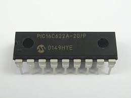
The W register is an 8-bit working register used for ALU operations. It is not an addressable register Depending on the instruction executed, the ALU may affect the values of the Carry (C), Digit Carry (DC), and Zero (Z) bits in the STATUS register. The C and DC bits operate as a Borrow and Digit Borrow out bit, respectively, bit in subtraction. See the SUBLW and SUBWF instructions for examples.
Our Service: Safe and Controlled Recovery of Embedded Software
We help businesses and engineers who need to break through inaccessible or obsolete MCU barriers to recover their own program files. Our objective is not unauthorized hacking but legitimate data restoration for owners who have lost the original design file or development archive.
Our service includes:
- Chip evaluation to confirm feasibility
- High-level security assessment before any attack or decode operation
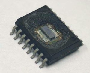
- Optional non-destructive techniques or advanced decapsulation, depending on chip condition
- Secure extraction of internal firmware, calibration data, or eeprom contents
- Output of a clean, validated binary or heximal program ready for production or system repair
All internal procedures remain confidential, and we do not share technical details of how protections are unlocked.
General Concept of the Recovery Process (Non-Technical Overview)
Recovering embedded software from a secured PIC16C622A involves precisely controlled steps that may include reading device states, analyzing memory integrity, and applying specialized methods to decode or retrieve protected data. The goal is always to preserve the original program while avoiding any physical damage to the chip.
Why End-Users Choose This Service
Customers depend on this recovery solution for several business-critical reasons:
- Reviving production lines when development source code is lost
- Eliminating high redesign costs for legacy devices
- Ensuring long-term serviceability for field-deployed equipment
- Restoring intellectual property already paid for and designed internally
- Maintaining competitive advantage by controlling system logic
The ability to clone or duplicate the recovered firmware ensures product continuity without forced redesign.
Technical Challenges You Might Encounter
Some PIC16C622A units exhibit difficulties such as worn flash, degraded memory, heavy encrypted protections, or complex protective configurations. These conditions require precise handling to avoid partial or corrupted data output. Our team is experienced in processing such cases with the highest reliability.
Attack Microcontroller PIC16C710 Program
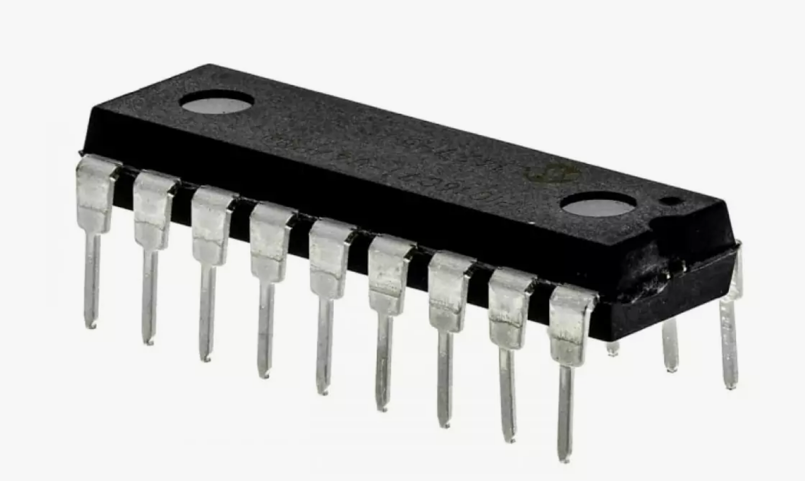
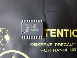
The Microchip PIC16C710 remains widely used in industrial controllers, home appliances, automotive interfaces, low-power automation boards, and specialized embedded modules. Over time, many companies face the challenge of maintaining or replicating systems built around this MCU, only to discover that the internal program, calibration data, or configuration eeprom cannot be accessed due to protected, encrypted, or fully locked security mechanisms. Our dedicated service under the subject Attack Microcontroller PIC16C710 Program is built specifically to help legitimate device owners retrieve and secure the original firmware when conventional development files or source code are no longer available.
Why the PIC16C710 Is Still Important Across Industries
Although it is part of an earlier generation of Microchip devices, the PIC16C710 offers dependable performance, integrated analog functionality, compact architecture, and stable embedded flash technology. These traits make it ideal for:
- Consumer electronic modules and appliance control boards
- Analog measurement devices and sensor processing units
- Automotive accessory drivers and interface systems
- Machine automation modules and industrial control panels
- Legacy devices that rely on highly customized logic
The internal binary and heximal code inside the PIC16C710 is often the heart of the product’s functional design—meaning that losing it can completely halt production or repair capabilities.
Our Service: Controlled Recovery of Protected Firmware
We provide specialized assistance to customers who need to break the barrier of inaccessible memory and safely retrieve, clone, or duplicate the MCU’s file contents. Our service focuses on legitimate recovery—never unauthorized hacking—and is structured to help owners restore what rightfully belongs to them.
What we offer includes:
- Non-destructive analysis of the chip’s protection state
- Controlled operations that may include chip-level evaluation or optional decapsulation, depending on condition
- Secure extraction of internal program, calibration memory, or eeprom
- Delivery of clean, verified firmware images suitable for future production or redesign
All technical processes remain confidential; we do not reveal how protections are bypassed or how decoding mechanisms function. We ensure compliance, safety, and professional handling.
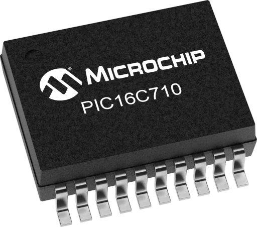
We can Attack Microcontroller PIC16C710 Program, please view the Microcontroller PIC16C710 features for your reference:
PIC16C71X Microcontroller Core Features:
· High-performance RISC CPU
· Only 35 single word instructions to learn
· All single cycle instructions except for program branches which are two cycle
· Operating speed: DC – 20 MHz clock input DC – 200 ns instruction cycle
· Up to 2K x 14 words of Program Memory, up to 128 x 8 bytes of Data Memory (RAM)
· Interrupt capability
· Eight level deep hardware stack
· Direct, indirect, and relative addressing modes
· Power-on Reset (POR)
· Power-up Timer (PWRT) and Oscillator Start-up Timer (OST)
· Watchdog Timer (WDT) with its own on-chip RC oscillator for reliable operation;
· Programmable code-protection
· Power saving SLEEP mode
· Selectable oscillator options
· Low-power, high-speed CMOS EPROM technology
· Fully static design
· Wide operating voltage range: 2.5V to 6.0V
· High Sink/Source Current 25/25 mA
· Commercial, Industrial and Extended temperature ranges
· Program Memory Parity Error Checking Circuitry
with Parity Error Reset (PER) (PIC16C715)
· Low-power consumption:
– < 2 mA @ 5V, 4 MHz
– 15 µA typical @ 3V, 32 kHz
– < 1 µA typical standby current
General Concept of the Recovery Process (High-Level Explanation Only)
Each PIC16C710 device undergoes a detailed preliminary check to determine the feasibility of recovery. Once confirmed, carefully orchestrated operations are performed to decode or access the internal archive without compromising memory integrity. The final output typically includes a binary or heximal dump that can be used to reprogram new units or verify system logic.
Why Clients Depend on This Service
Companies and engineers rely on our service to:
- Continue manufacturing products after losing original source code
- Rebuild or update legacy systems without redesigning from zero
- Reduce downtime caused by obsolete or discontinued MCUs
- Protect their technical investments and keep service departments operational
- Maintain strategic control over product functionality for the long term
Our ability to attack secured microcontrollers legally and professionally ensures business continuity and engineering independence.
Possible Challenges During Recovery
Some PIC16C710 units present more complex issues, such as degraded memory, ultra-tight secured configurations, or device aging that affects reliability. These conditions require specialized handling to guarantee a stable and complete firmware output.
Attack MCU PIC16F711 Heximal
Embedded systems built on the Microchip PIC16F711 microcontroller are widely deployed in industrial automation, automotive subsystems, consumer electronics, and sensor-based applications. Over time, these systems often become inaccessible due to protected, locked, or encrypted firmware configurations, preventing rightful owners from maintaining or updating their equipment. Our specialized service, centered on the keyword Attack MCU PIC16F711 Heximal, provides a secure, authorized solution to retrieve, clone, and restore embedded program files, binary data, and heximal archives—without disclosing proprietary technical methods.
The PIC16C71X family has special features to reduce external components, thus reducing cost, enhancing system reliability and reducing power consumption which is critical for Attack MCU PIC16F711 Heximal.
There are four oscillator options, of which the single pin RC oscillator provides a low-cost solution, the LP oscillator minimizes power consumption, XT is a standard crystal, and the HS is for High Speed crystals. The SLEEP (power-down) feature provides a power saving mode. The user can wake up the MCU from SLEEP through several external and internal interrupts and resets.
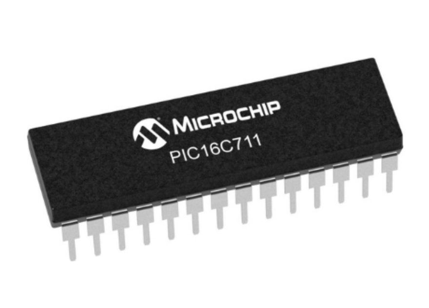
The PIC16F711 is a versatile 8-bit microcontroller known for its integrated analog-to-digital converters, compact design, and low-power operation. It is commonly found in:
- Industrial Control Modules: Sensor interfaces, motor controllers, and PLC peripherals.
- Automotive Electronics: Auxiliary control units, lighting systems, and diagnostic tools.
- Consumer Appliances: Power management systems, remote controls, and smart home devices.
- Medical Devices: Portable monitors and diagnostic equipment requiring reliable embedded control.
Its secured flash and EEPROM memory often store calibration data, operational logic, and configuration parameters critical to system functionality.
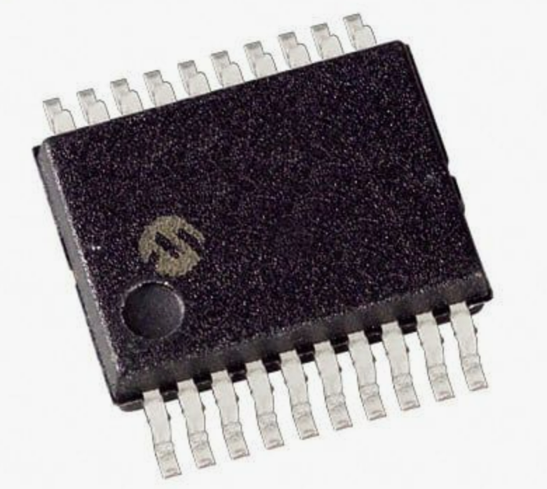
A highly reliable Watchdog Timer with its own on-MCU RC oscillator provides protection against software lock up. A UV erasable CERDIP packaged version is ideal for code development while the cost-effective One-Time-Programmable (OTP) version is suitable for production in any volume.
The PIC16C71X family fits perfectly in applications ranging from security and remote sensors to appliance control and automotive which is the reason for its MCU cracking. The EPROM technology makes customization of application programs (transmitter codes, motor speeds, receiver frequencies, etc.) extremely fast and convenient.
We assist clients in scenarios where firmware archives are lost, corrupted, or locked due to protective settings. Our end-to-end solution includes:
- Non-Destructive Analysis: Assessing the device’s security configuration and memory integrity.
- Controlled Extraction: Using advanced techniques to decode and retrieve the embedded heximal or binary program.
- Data Validation: Verifying the integrity of extracted firmware and eeprom data.
- Legal Compliance: Ensuring all work is conducted under authorization and confidentiality agreements.
We do not disclose methods to hack or decapsulate devices for unauthorized purposes. Instead, we deliver a validated file or archive that enables clients to duplicate, migrate, or restore their systems.
The small footprint packages make this microcontroller series perfect for all applications with space limitations. Low cost, low power, high performance, ease of use and I/O flexibility make the PIC16C71X very versatile even in areas where no microcontroller use has been considered before Attack MCU PIC16F711 Heximal (e.g. timer functions, serial communication, capture and compare, PWM functions and coprocessor applications).
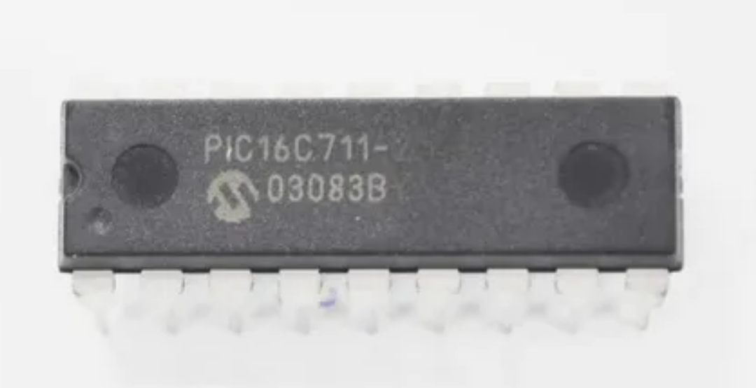
- Minimized Downtime: Rapid recovery of operational firmware keeps production lines and legacy systems running.
- IP Preservation: Safeguard proprietary source code and calibration data embedded in the microcontroller.
- Legacy System Support: Extend the lifespan of equipment reliant on obsolete or unsupported hardware.
- Authorized Cloning: Legally duplicate firmware for backup, scaling, or replacement units.
Users familiar with the PIC16C5X microcontroller family will realize that this is an enhanced version of the PIC16C5X architecture. Please refer to Appendix A for a detailed list of enhancements. Code written for the PIC16C5X can be easily ported to the PIC16CXX family of devices.
- Advanced Protections: Some PIC16F711 units employ layered encrypted or secured configurations.
- Hardware Degradation: Aging components may lead to partial memory corruption or read failures.
- Device Variants: Slight differences in silicon revisions can complicate extraction efforts.
Despite these challenges, our systematic approach maximizes success rates while prioritizing device integrity and data confidentiality. For organizations facing firmware accessibility issues with the PIC16F711, our service offers a reliable, ethical path to recover, clone, and preserve critical embedded data. By combining technical expertise with legal compliance, we help clients maintain operational continuity and protect their intellectual property.
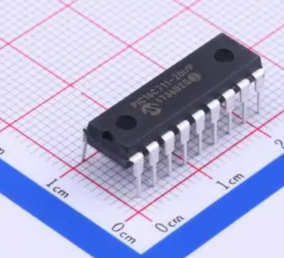
 Posted in Recover MCU |
  Tags: zaatakować mcu bin, zaatakować mcu code, zaatakować mcu data, zaatakować mcu eeprom, zaatakować mcu file, zaatakować mcu firmware, zaatakować mcu flash, zaatakować mcu hex, zaatakować mcu memory, zaatakować mcu program |
  Comments Closed
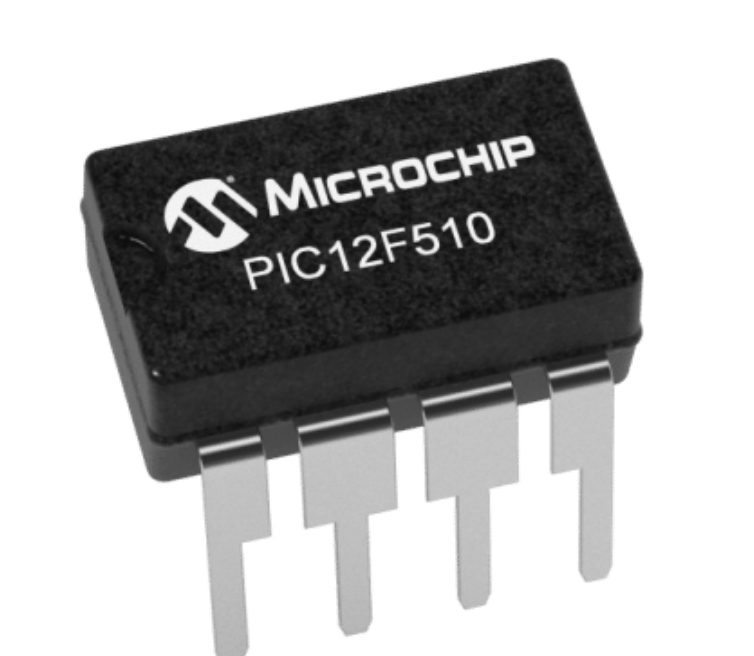
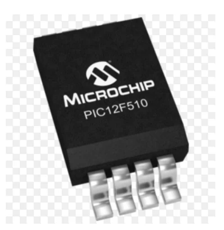
Attack IC PIC12F510 Program
Electronic systems built around the Microchip PIC12F510 microcontroller continue to operate in industrial equipment, compact control modules, consumer electronics, sensor hardware, and smart automation devices worldwide. As these systems mature, owners frequently discover that the internal program, calibration data, or eeprom configuration cannot be accessed due to encrypted, protected, or fully locked security settings. Our advanced service, operating under the subject Attack IC PIC12F510 Program, is designed to assist legitimate system owners with retrieving and safeguarding valuable firmware from this device when no alternative documentation or original source code exists.
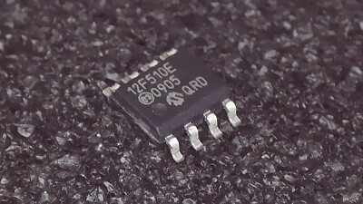
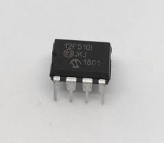
We can Attack IC PIC12F510 Program, please view the IC PIC12F510 features for your reference:
High-Performance RISC CPU:
· Only 33 single-word instructions to learn
· All single-cycle instructions except for program branches, which are two-cycle
· 12-bit wide instructions
· 2-level deep hardware stack
· Direct, Indirect and Relative Addressing modes for data and instructions
· 8-bit wide data path
Why PIC12F510 Matters in Modern and Legacy Systems
The PIC12F510 is a compact and highly efficient embedded microcontroller with an 8-bit architecture, onboard oscillator, and dedicated flash storage. Despite its small footprint, it supports a wide range of automation and control functions. It is widely deployed in:
- Smart sensors and IoT-style low-power modules
- Consumer electronic controllers and accessories
- Industrial interface boards and portable tools
- Compact robotics, power drivers, and lighting products
- Entry-level programmable devices used in educational engineering
Manufacturers often rely on custom-developed logic stored within the internal binary or heximal image, making the internal archive extremely valuable.
· 10 Special Function Hardware registers (PIC12F510)
· 13 Special Function Hardware registers (PIC16F506)
· Operating speed:
– DC – 8 MHz Crystal Oscillator (PIC12F510)
– DC – 500 ns instruction cycle (PIC12F510)
– DC – 20 MHz Crystal Oscillator (PIC16F506)
– DC – 200 ns instruction cycle (PIC16F506)
Special Microcontroller Features:
· 4 or 8 MHz selectable precision internal oscillator
– Factory calibrated to ±1%
· In-Circuit Serial Programming™ (ICSP™)
· In-Circuit Debugging (ICD) support
· Power-on Reset (POR)
· Device Reset Timer (DRT):
– Short DRT (1.125 ms, typical) for INTOSC, EXTRC and EC
– DRT (18 ms, typical) for HS, XT and LP
· Watchdog Timer (WDT) with dedicated on-chip RC oscillator for reliable operation
· Programmable code protection
· Multiplexed MCLR input pin
What Our Service Provides
Our role is to assist organizations or authorized owners who need to break through inaccessible security layers and safely extract the embedded file containing the functional logic of the device. We provide a full solution covering:
- Controlled evaluation of chip condition and security level
- Secure retrieve, clone, or duplicate memory output for approved clients
- Preservation of internal program and calibration memory
- Reconstruction of missing engineering documentation for long-term maintenance
While some cases require advanced measurement or optional decapsulation, we never disclose technical methodology. Our focus is on compliance, confidentiality, and precision—not teaching users how to hack or decode hardware protections on their own.
· Selectable internal weak pull-ups on I/O pins
· Power-Saving Sleep mode
· Wake-up from Sleep on pin change
· Wake-up from Sleep on comparator change
· Selectable oscillator options:
– INTOSC: 4/8 MHz precision Internal oscillator
– EXTRC: External low-cost RC oscillator
– XT: Standard crystal/resonator
– LP: Power-saving, low-frequency crystal
– HS: High-speed crystal/resonator (PIC16F506 only)
– EC: High-speed external clock input (PIC16F506 only)
· Analog-to-Digital (A/D) Converter:
– 8-bit resolution
General Recovery Approach (Non-Technical and Safe)
Each PIC12F510 is assessed based on its configuration state, environmental condition, and secured parameters. Once feasibility is confirmed, controlled extraction operations are performed to recover the internal firmware in a stable and verifiable format. After recovery, clients receive a clean binary or heximal memory image suitable for redevelopment, migration, or duplication into new hardware.
– 4-input channels (1 channel is dedicated to conversion of the internal 0.6V absolute voltage reference)
· High current sink/source for direct LED drive
· 8-bit real-time clock/counter (TMR0) with 8-bit programmable prescaler
Low-Power Features/CMOS Technology:
· Operating Current:
– < 170 ìA @ 2V, 4 MHz
· Standby Current:
– 100 nA @ 2V, typical
· Low-power, high-speed Flash technology:
– 100,000 cycle Flash endurance
– > 40-year retention
· Fully static design
· Wide operating voltage range: 2.0V to 5.5V
· Wide temperature range:
– Industrial: -40°C to +85°C
– Extended: -40°C to +125°C
Peripheral Features (PIC12F510):
· 6 I/O pins:
– 5 I/O pins with individual direction control
– 1 input only pin
· 1 Analog Comparator with absolute reference
Peripheral Features (PIC16F506):
· 12 I/O pins:
– 11 I/O pins with individual direction control
– 1 input only pin
· 2 Analog Comparators with absolute reference and programmable reference .
8-bit resolution
– 4-input channels (1 channel is dedicated to conversion of the internal 0.6V absolute voltage reference)
· High current sink/source for direct LED drive
· 8-bit real-time clock/counter (TMR0) with 8-bit programmable prescaler
Low-Power Features/CMOS Technology:
· Operating Current:
– < 170 ìA @ 2V, 4 MHz
· Standby Current:
– 100 nA @ 2V, typical
· Low-power, high-speed Flash technology:
– 100,000 cycle Flash endurance
– > 40-year retention
· Fully static design
· Wide operating voltage range: 2.0V to 5.5V
· Wide temperature range:
– Industrial: -40°C to +85°C
– Extended: -40°C to +125°C
Benefits to the End User
Clients choose this service because it allows them to:
- Continue production when the original developer or supplier is unavailable
- Protect operational investments tied to legacy microcontroller platforms
- Avoid rewriting devices from scratch due to lost source code
- Maintain or redesign systems without unknown programming risks
- Build a controlled archive for future engineering and servicing
This ensures long-term sustainability, reduced operational cost, and business continuity.
Attack IC PIC16F54 Eeprom
We can attack IC PIC16F54 Eeprom, please view the IC PIC16F54 features for your reference:
High-Performance RISC CPU:
· Only 33 single-word instructions to learn
· All instructions are single cycle except for program branches which are two-cycle
· Two-level deep hardware stack
· Direct, Indirect and Relative Addressing modes for data and instructions
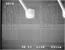
Attack IC PIC16F54 Eeprom
· Operating speed:
– DC – 20 MHz clock speed
– DC – 200 ns instruction cycle time
· On-ic Flash program memory:
– 512 x 12 on PIC16F54
– 2048 x 12 on PIC16F57
– 2048 x 12 on PIC16F59
· General Purpose Registers (SRAM)
– 25 x 8 on PIC16F54
– 72 x 8 on PIC16F57
– 134 x 8 on PIC16F59
Special Microcontroller Features:
· Power-on Reset (POR)
· Device Reset Timer (DRT)
· Watchdog Timer (WDT) with its own on-ic RC oscillator for reliable operation
· Programmable Code Protection to prevent Microcontroller unlocking
· Power-Saving Sleep mode
· In-Circuit Serial Programming™ (ICSP™)
· Selectable oscillator options:
– RC: Low-cost RC oscillator
– XT: Standard crystal/resonator
– HS: High-speed crystal/resonator
– LP: Power-saving, low-frequency crystal
· Packages:
– 18-pin PDIP and SOIC for PIC16F54
– 20-pin SSOP for PIC16F54
– 28-pin PDIP, SOIC and SSOP for PIC16F57
– 40-pin PDIP for PIC16F59
– 44-pin TQFP for PIC16F59
Low-Power Features:
· Operating Current:
– 170 ìA @ 2V, 4 MHz, typical
– 15 ìA @ 2V, 32 kHz, typical
· Standby Current:
– 500 nA @ 2V, typical
Peripheral Features:
· 12/20/32 I/O pins:
– Individual direction control
– High current source/sink
· 8-bit real-time clock/counter (TMR0) with 8-bit programmable prescaler
CMOS Technology:
· Wide operating voltage range:
– Industrial: 2.0V to 5.5V
– Extended: 2.0V to 5.5V
· Wide temperature range:
– Industrial: -40°C to 85°C
– Extended: -40°C to 125°C
· High-endurance Flash:
– 100K write/erase cycles
– > 40-year retention
Attack Chip DSP TMS320LF2406APZAR Flash
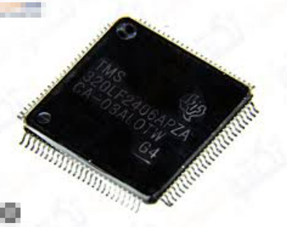
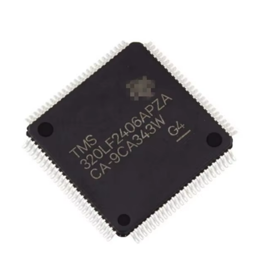
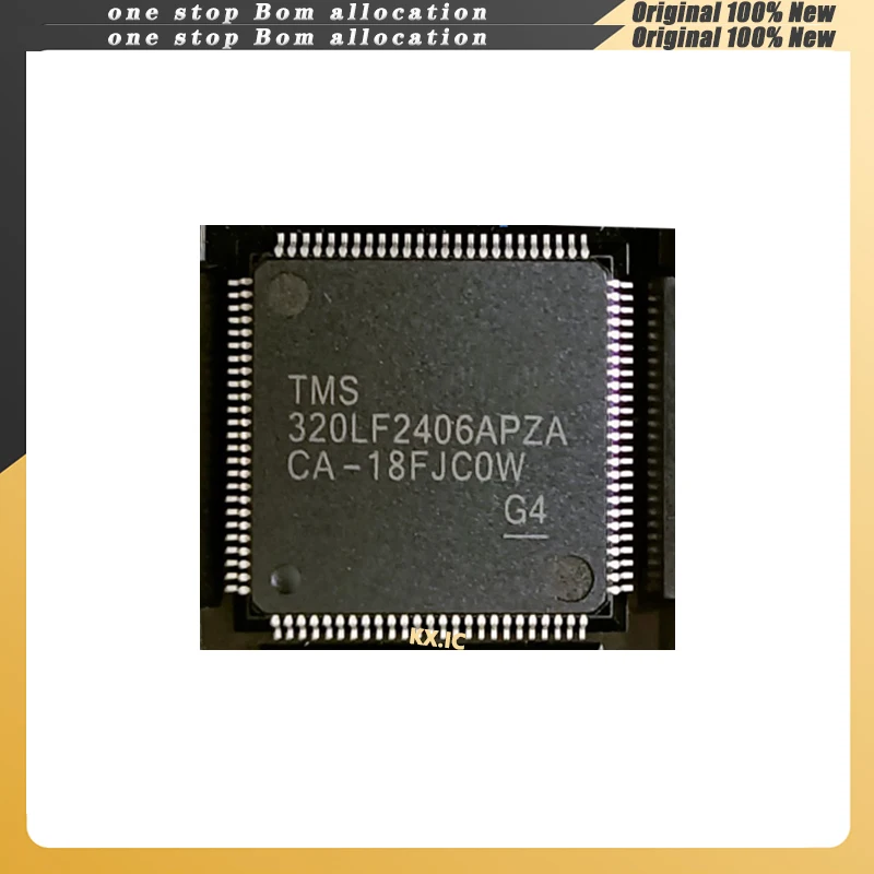
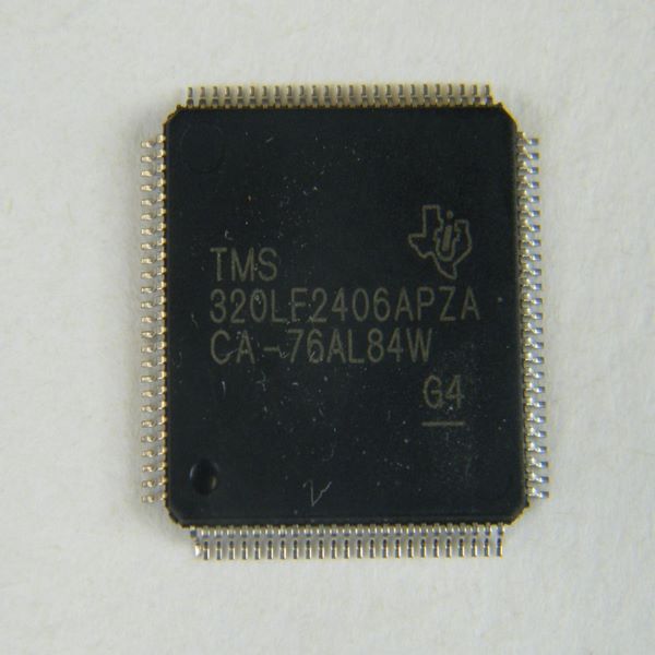
The Texas Instruments TMS320LF2406APZAR is a member of the TMS320 family of digital signal processors (DSPs) widely used where deterministic control and high-performance numeric processing are required. When the flash memory of such a device becomes protected, locked, or otherwise inaccessible, organizations may need a trusted partner to attack chip DSP TMS320LF2406APZAR flash in order to readout, recover, restore, or duplicate the embedded firmware/binary/heximal program. Our service provides lawful, confidential support to help end users regain access to their program files/archives without revealing technical bypass methods.
Why this service matters
Devices driven by the TMS320LF2406APZAR commonly contain mission-critical programs, calibration data, and timing-sensitive control algorithms. Legitimate reasons for requesting recovery include: restoring corrupted flash after failures, duplicating firmware for authorized spares provisioning, migrating legacy systems to new hardware, or performing authorized security audits. In each case, recovered binary or heximal images can be essential to get equipment back online and preserve operational continuity.
Where the chip is used
This DSP is often found in demanding applications such as:
- Motor control and servo systems (industrial drives, robotics).
- Power electronics (inverters, converters, UPS systems).
- Renewable energy equipment (solar/wind converters).
- Advanced instrumentation and embedded measurement systems.
Because these markets require precision and reliability, firmware on these devices is commonly treated as a secured asset and sometimes configured with protective settings.
What we offer (high level, non-actionable)
Our engagements are focused on authorized recovery and analysis. Services include:
- Validated extraction of on-chip images where permitted, producing verified heximal or binary dumps.
- Non-destructive handling and validation to preserve device integrity and avoid data loss.
- High-level decoding and annotated disassembly summaries to help engineers understand recovered program logic (without providing instructions to bypass protections).
- Delivery of recovered files and clear documentation to support restoration, duplication, or migration efforts.
We require proof of ownership or explicit authorization for all work and operate under strict confidentiality agreements.
General (conceptual) approach
A responsible project begins with verification and a risk assessment, followed by careful, conservative recovery attempts. The goal is to obtain a reliable archive of the device’s memory and then translate raw data into a usable representation for maintenance, testing, or authorized redevelopment. We do not disclose or provide instructions for circumventing manufacturer security measures.
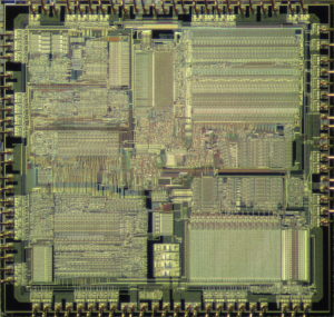
We can Attack Chip DSP TMS320LF2406APZAR Flash, below is the Chip DSP TMS320LF2406APZAR features for your reference:
High-Performance Static CMOS Technology
− 25-ns Instruction Cycle Time (40 MHz)
− 40-MIPS Performance
− Low-Power 3.3-V Design
D Based on TMS320C2xx DSP CPU Core
− Code-Compatible With F243/F241/C242
− Instruction Set and Module Compatible With F240 D Flash (LF) and ROM (LC) Device Options
− LF240xA: LF2407A, LF2406A, LF2403A, LF2402A
− LC240xA: LC2406A, LC2404A, LC2403A, LC2402A D On-Chip Memory
− Up to 32K Words x 16 Bits of Flash EEPROM (4 Sectors) or ROM
− Programmable “Code-Security” Feature for the On-Chip Flash/ROM
− Up to 2.5K Words x 16 Bits of Data/Program RAM
− 544 Words of Dual-Access RAM
− Up to 2K Words of Single-Access RAM D Boot ROM (LF240xA Devices)
− SCI/SPI Bootloader D Up to Two Event-Manager (EV) Modules (EVA and EVB), Each Includes:
− Two 16-Bit General-Purpose Timers
− Eight 16-Bit Pulse-Width Modulation (PWM) Channels Which Enable:
− Three-Phase Inverter Control can be used for MCU Cracking
− Center- or Edge-Alignment of PWM Channels
− Emergency PWM Channel Shutdown With External PDPINTx Pin
− Programmable Deadband (Deadtime) Prevents Shoot-Through Faults
− Three Capture Units for Time-Stamping of External Events
− Input Qualifier for Select Pins
− On-Chip Position Encoder Interface Circuitry
− Synchronized A-to-D Conversion
− Designed for AC Induction, BLDC, Switched Reluctance, and Stepper Motor
Control
− Applicable for Multiple Motor and/or Converter Control
D External Memory Interface (LF2407A)
− 192K Words x 16 Bits of Total Memory:
64K Program, 64K Data, 64K I/O
D Watchdog (WD) Timer Module
D 10-Bit Analog-to-Digital Converter (ADC)
− 8 or 16 Multiplexed Input Channels
− 500-ns MIN Conversion Time
− Selectable Twin 8-State Sequencers
Triggered by Two Event Managers
D Controller Area Network (CAN) 2.0B Module
(LF2407A, 2406A, 2403A)
D Serial Communications Interface (SCI)
D 16-Bit Serial Peripheral Interface (SPI) (LF2407A, 2406A, LC2404A, 2403A)
D Phase-Locked-Loop (PLL)-Based Clock
Generation
D Up to 40 Individually Programmable, Multiplexed General-Purpose Input / Output (GPIO) Pins
D Up to Five External Interrupts (Power Drive Protection, Reset, Two Maskable Interrupts)
D Power Management:
− Three Power-Down Modes
− Ability to Power Down Each Peripheral Independently
D Real-Time JTAG-Compliant Scan-Based Emulation, IEEE Standard 1149.1† (JTAG)
D Development Tools Include:
− Texas Instruments (TI) ANSI C Compiler, Assembler/ Linker, and Code Composer Studio Debugger
− Evaluation Modules
− Scan-Based Self-Emulation (XDS510)
− Broad Third-Party Digital Motor Control Support
D Package Options
− 144-Pin LQFP PGE (LF2407A)
− 100-Pin LQFP PZ (2406A, LC2404A)
− 64-Pin TQFP PAG (LF2403A, LC2403A, LC2402A)
− 64-Pin QFP PG (2402A) D Extended Temperature Options (A and S)
− A: − 40°C to 85°C
− S: − 40°C to 125°C
Clients who use this service can expect reduced downtime, secure backups of previously inaccessible firmware, and the ability to maintain or scale legacy platforms. Recovered program data enables authorized cloning, duplication, and migration—helping preserve product lifecycles and protect investment in specialized hardware.
Challenges and limitations
Recovery from DSPs like the TMS320LF2406APZAR can be complex due to proprietary memory maps, layered protections, partial data corruption, or checksum/integrity checks. Not every recovery yields source-level code; sometimes only binary/heximal archives and assembly-level annotations are recoverable. We evaluate feasibility up front and keep clients informed about likely outcomes.
Legal & ethical safeguards
All projects are undertaken only after proper authorization and under legal agreements. Our focus is to unlock, restore, or duplicate firmware for legitimate, constructive purposes—repair, continuity, authorized audit, and migration—while protecting intellectual property and safety.
If you need help to Attack Chip DSP TMS320LF2406APZAR Flash for lawful recovery or maintenance, our experienced team provides confidential, professional support to retrieve and document embedded program data while safeguarding your assets and operations.
Attack Microcontroller TMS320C32PCM40 Firmware
Attack Microcontroller TMS320C32PCM40 Firmware
We can Attack Microcontroller TMS320C32PCM40 Firmware, please view below Microcontroller TMS320C32PCM40 features for your reference:
High-Performance Floating-Point DSP
– TMS320C32-60 (5 V)
33-ns Instruction Cycle Time
330 Million Operations Per Second (MOPS), 60 Million Floating-Point Operations Per Second (MFLOPS), 30 Million Instructions Per Second (MIPS)
– TMS320C32-50 (5 V)
40-ns Instruction Cycle Time
275 MOPS, 50 MFLOPS, 25 MIPS
– TMS320C32-40 (5 V)
50-ns Instruction Cycle Time 220 MOPS, 40 MFLOPS, 20 MIPS
32-Bit High-Performance CPU
16- / 32-Bit Integer and 32- / 40-Bit
Floating-Point Operations
32-Bit Instruction Word, 24-Bit Addresses
Two 256 × 32-Bit Single-Cycle, Dual-Access
On-Chip RAM Blocks
Flexible Boot-Program Loader to Unlocking Microcontroller
On-Chip Memory-Mapped Peripherals:
– One Serial Port
– Two 32-Bit Timers
– Two-Channel Direct Memory Access (DMA) Coprocessor With Configurable Priorities
Enhanced External Memory Interface That Supports 8- / 16- / 32-Bit-Wide External RAM for Data Access and Program Execution From 16- / 32-Bit-Wide External RAM
TMS320C30 and TMS320C31 Object Code Compatible Fabricated using 0.7 µm Enhanced Performance Implanted CMOS (EPIC)
Technology by Texas Instruments (TI) 144-Pin Plastic Quad Flat Package ( PCM Suffix ) 5 V Eight Extended-Precision Registers
Two Address Generators With Eight
Auxiliary Registers and Two Auxiliary
Register Arithmetic Units (ARAUs)
Two Low-Power Modes
Two- and Three-Operand Instructions
Parallel Arithmetic Logic Unit (ALU) and
Multiplier Execution in a Single Cycle
Block-Repeat Capability
Zero-Overhead Loops With Single-Cycle
Branches
Conditional Calls and Returns
Interlocked Instructions for
Multiprocessing Support
One External Pin, PRGW, That Configures the External-Program-Memory Width to 16 or 32 Bits
Two Sets of Memory Strobes (STRB0 and STRB1) and One I / O Strobe (IOSTRB)
Allow Zero-Glue Logic Interface to Two
Banks of Memory and One Bank of External
Peripherals
Separate Bus-Control Registers for Each
Strobe-Control Wait-State Generation,
External Memory Width, and Data Type Size
STRB0 and STRB1 Memory Strobes Handle 8-, 16-, or 32-Bit External Data Accesses (Reads and Writes)
Multiprocessor Support Through the HOLD and HOLDA Signals Is Valid for All Strobes
Posted in Recover MCU |
Tags: знаходзіць зноў locked ic binary, знаходзіць зноў locked ic data, знаходзіць зноў locked ic eeprom, знаходзіць зноў locked ic file, знаходзіць зноў locked ic firmware, знаходзіць зноў locked ic flash, знаходзіць зноў locked ic heximal, знаходзіць зноў locked ic memory, знаходзіць зноў locked ic program |
Comments Closed
Attack MCU TMS320F241PG Heximal
When a device relies on a Texas Instruments DSP such as the TMS320F241PG, the firmware stored in its on-chip memory is often the heart of the system — controlling timing, signal processing, and safety-critical loops. Our service, searchable under the keyword Attack MCU TMS320F241PG Heximal, helps authorized users restore, readout, decode, and recover the firmware/binary/heximal program and data from these protected or locked devices. We focus on lawful, confidential work that returns usable program images and high-level analysis without enabling misuse.
Legitimate needs to open, copy, clone, duplicate, or restore TMS320F241PG firmware commonly include: repairing equipment after firmware corruption; backing up archived program files for legacy support; migrating control software to replacement hardware; performing security audits; and recovering crucial calibration data or configuration archives. In many industrial settings, losing access to the embedded program can mean costly downtime — so secure recovery is essential.
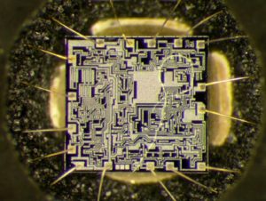
We can Attack MCU TMS320F241PG Heximal, please view the MCU TMS320F241PG features below for your reference:
High-Performance Static CMOS Technology
D Includes the T320C2xx Core CPU
– Object-Compatible With the TMS320C2xx
– Source-Code-Compatible With TMS320C25
D Single 10-Bit Analog-to-Digital Converter
(ADC) Module With 8 Multiplexed Input Channels
D 26 Individually Programmable, Multiplexed
General-Purpose I / O (GPIO) Pins
– Upwardly Compatible With TMS320C5x
– 50-ns Instruction Cycle Time
Pin Compatible to Emulation Device
TMS320F241 (64-Pin/68-Pin)
Code Compatible to Emulation Devices TMS320F243 and TMS320F241
Commercial and Industrial Temperature Available
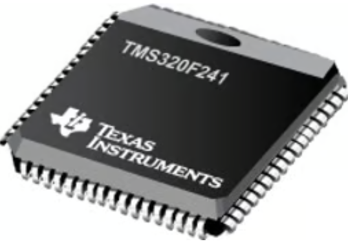
Memory
– 544 Words x 16 Bits of On-Chip Data/Program Dual-Access RAM (DARAM)
– 4K Words x 16 Bits of On-chip Program ROM Event-Manager Module
– Eight Compare/ Pulse-Width Modulation (PWM) Channels
– Two 16-Bit General-Purpose Timers With Six Modes, Including Continuous Up and Up / Down Counting
– Three 16-Bit Full Compare Units With Phase-Locked-Loop (PLL)-Based Clock Watchdog (WD) Timer Module
Serial Communications Interface (SCI);
Five External Interrupts (Power Drive Protection, Reset, NMI, and Two Maskable Interrupts)
Three Power-Down Modes for Low-Power
Operation
Scan-Based Emulation
Development Tools Available:
– Texas Instruments (TI) ANSI Compiler, Assembler / Linker, and
C-Source Debugger
– Full Range of Emulation Products
– Self-Emulation (XDS510)
– Third-Party Digital Motor Control and Fuzzy-Logic Development Support
68-Pin PLCC FN Package
64-Pin QFP PG Package
Deadband
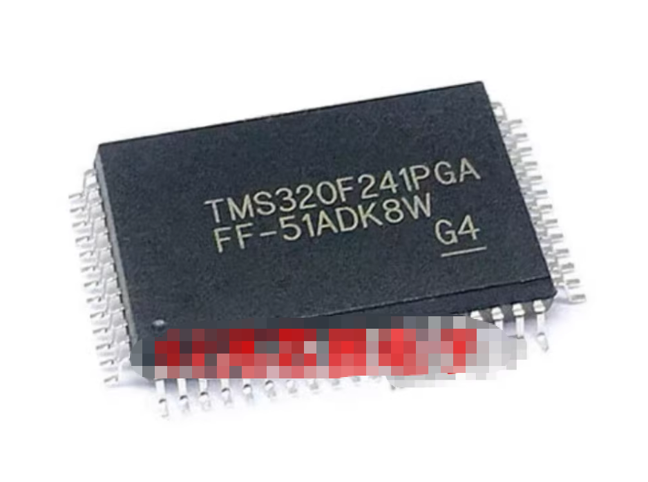
– Three Capture Units (Two With Quadrature Encoder-Pulse Interface Capability)
TMS320C2xx generation of 16-bit fixed-point DSPs.
The TMS320F241 device is fully compatible with the C242 to allow emulation during prototype development. (These two devices share similar core and peripherals.) This new family is optimized for digital motor / motion control applications
The DSP controllers combine the enhanced TMS320 architectural design of the ’C2xx core CPU for low-cost, high-performance processing capabilities and several advanced peripherals optimized for motor/motion control applications, These peripherals include the event manager module, which provides general-purpose timers and PWM registers to generate PWM outputs, and a single,10-bit analog-to-digital converter (ADC), which can perform conversion within 1 µs.
The TMS320 family and its variants like the F241PG are widely used across industries that require deterministic, high-performance signal processing and control:
- Motor drives and servo controllers (precision torque/speed loops).
- Power conversion and inverter systems (renewables, UPS, power supplies).
- Industrial automation (motion controllers, PLC peripherals).
- Advanced instrumentation and measurement systems requiring fast DSP math.
Because these applications often incorporate calibration tables, control algorithms, and safety logic, the flash/EEPROM contents are frequently treated as protected or secured assets.
What we provide (high level, non-actionable)
Our engagement is built around safe, authorized firmware recovery and analysis. Typical services include:
- Verified extraction of raw binary/heximal images from on-chip memory where permitted.
- Non-destructive validation and checksum checks of extracted archives.
- High-level disassembly and annotated summaries that convert raw dumps into readable assembly-level views and contextual commentary (not step-by-step bypass instructions).
- Support to restore devices to operation using recovered firmware, and assistance preparing migration packages for replacement hardware.
- Confidential handling and delivery of recovered program files and documented reports.
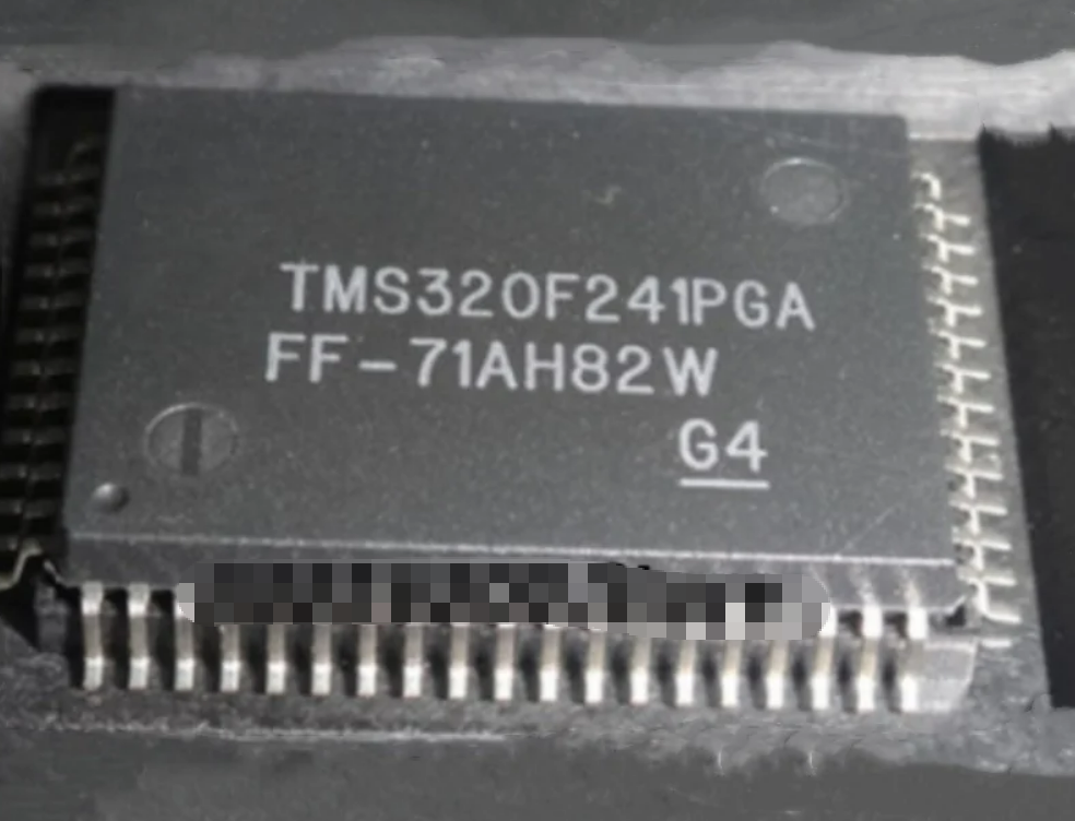
We do not provide step-by-step guidance for illegally circumventing manufacturer protections, nor do we assist unauthorized copying or distribution of copyrighted or safety-critical code.
General idea of the workflow (conceptual)
A responsible recovery project typically begins with device and chip identification, verification of ownership/authorization, and a risk assessment. Engineers then attempt non-destructive readout and validate the integrity of the extracted memory image. Once a stable dump is obtained, analysis and decoding transform the raw data into an intelligible program representation and recovery artifacts that customers can use for testing, repair, or redeployment.
Benefits and expected outcomes
Clients gain reduced downtime, secure backups of previously inaccessible firmware, and the ability to maintain and support legacy systems. Recovered heximal or binary files enable replication, authorized cloning, and safer migration strategies — all under controlled, legal terms.
Difficulties you may encounter
Challenges include layered manufacturer protections, partial data corruption, device variants with different memory maps, and the presence of proprietary encryption or integrity checks. Not all recoveries yield full source-level clarity; in many cases, only the binary/heximal archives and assembly-level annotations are recoverable.
Ethics, authorization & confidentiality
All projects require proof of ownership or explicit authorization. Work is performed under strict confidentiality and legal agreements; our goal is to unlock and restore embedded systems for legitimate, constructive purposes only.
If you need to Attack MCU TMS320F241PG Heximal for lawful recovery, migration, or audit, our team provides secure, professional support to retrieve and document embedded firmware while protecting your IP and operational continuity.
Attack IC TMS320BC57 Flash
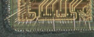
Attack IC TMS320BC57 Flash
We can Attack IC TMS320BC57 Flash, please view below IC TMS320BC57 features for your reference:
Powerful 16-Bit TMS320C5x CPU 20-, 25-, 35-, and 50-ns Single-Cycle
Instruction Execution Time for 5-V
Operation
25-, 40-, and 50-ns Single-Cycle Instruction
Execution Time for 3-V Operation
Single-Cycle 16 × 16-Bit Multiply/Add 224K × 16-Bit Maximum Addressable
External Memory Space (64K Program, 64K
Data, 64K I/O, and 32K Global)
2K, 4K, 8K, 16K, 32K × 16-Bit Single-Access
On-Chip Program ROM
1K, 3K, 6K, 9K × 16-Bit Single-Access
On-Chip Program / Data RAM (SARAM)
1K Dual-Access On-Chip Program / Data
RAM (DARAM)
Full-Duplex Synchronous Serial Port for Coder/Decoder Interface to crack MCU
Time-Division-Multiplexed (TDM) Serial Port
Hardware or Software Wait-State
Generation Capability
On-Chip Timer for Control Operations
Repeat Instructions for Efficient Use of
Program Space
Buffered Serial Port
Host Port Interface
Multiple Phase-Locked Loop (PLL)
Clocking Options (×1, ×2, ×3, ×4, ×5, ×9
Depending on Device)
Block Moves for Data/Program
Management
On-Chip Scan-Based Emulation Logic
Boundary Scan
Five Packaging Options
– 100-Pin Quad Flat Package (PJ Suffix)
– 100-Pin Thin Quad Flat Package (PZ Suffix)
– 128-Pin Thin Quad Flat Package (PBK Suffix)
– 132-Pin Quad Flat Package (PQ Suffix)
– 144-Pin Thin Quad Flat Package (PGE Suffix)
Low Power Dissipation and Power-Down
Modes:
– 47 mA (2.35 mA / MIP) at 5 V, 40-MHz Clock (Average)
– 23 mA (1.15 mA / MIP) at 3 V, 40-MHz
Description
The TMS320C5x generation of the Texas Instruments (TI ) TMS320 digital signal processors (DSPs) is fabricated with static CMOS integrated circuit technology; the architectural design is based upon that of an earlier TI DSP, the TMS320C25. The combination of advanced Harvard architecture, on-chip peripherals, on-chip memory, and a highly specialized instruction set is the basis of the operational flexibility and speed of the ’C5x‡ devices. They execute up to 50 million instructions per second (MIPS).
The ’C5x devices offer these advantages: Enhanced TMS320 architectural design for increased performance and versatility Modular architectural design for fast development of spin-off devices Advanced integrated-circuit processing technology for increased performance Upward-compatible source code (source code for ’C1x and ’C2x DSPs is upward compatible with ’C5x DSPs.) Enhanced TMS320 instruction set for faster algorithms and for optimized high-level language operation New static-design techniques for minimizing power consumption and maximizing radiation tolerance Clock (Average).
– 10 mA at 5 V, 40-MHz Clock (IDLE1 Mode)
– 3 mA at 5 V, 40-MHz Clock (IDLE2 Mode)
– 5 µA at 5 V, Clocks Off (IDLE2 Mode)
High-Performance Static CMOS Technology
IEEE Standard 1149.1† Test-Access Port (JTAG)
Posted in Recover MCU |
Tags: капіраваць ic binary, капіраваць ic code, капіраваць ic data, капіраваць ic eeprom, капіраваць ic file, капіраваць ic firmware, капіраваць ic heximal, капіраваць ic memory, капіраваць ic program |
Comments Closed
Attack Chip ST62T00CB6 Firmware
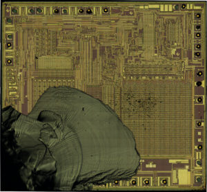
Attack Chip ST62T00CB6 Firmware
We can Attack Chip ST62T00CB6 Firmware and extract its source code out of eeprom, please view below Chip ST62T00CB6 features for your reference:
Memories
– 1K or 2K bytes Program memory (OTP, EPROM, FASTROM or ROM) with read-out protection
– 64 bytes RAM
Clock, Reset and Supply Management
– Enhanced reset system
PDIP16
– Low voltage detector (LVD) for safe Reset and Crack MCU
– Clock sources: crystal/ceramic resonator or RC network, external clock, backup oscillator (LFAO)
– Oscillator safeguard (OSG)
SO16
– 2 Power saving modes: Wait and Stop
Interrupt Management
– 4 interrupt vectors plus NMI and RESET
– 9 external interrupt lines (on 2 vectors)
SSOP16
9 I/O Ports
– 9 multifunctional bidirectional I/O lines
– 4 alternate function lines
– 3 high sink outputs (20mA)
2 Timers
– Configurable watchdog timer
CDIP16W
– 8-bit timer/counter with a 7-bit prescaler
Analog Peripheral
(See Section 11.5 for Ordering Information)
– 8-bit ADC with 4 input channels (except on ST6203C) Instruction Set
Development Tools
– Full hardware/software development package
– 8-bit data manipulation
– 40 basic instructions
– 9 addressing modes
– Bit manipulation
Posted in Recover MCU |
Tags: ламаць чып binary, ламаць чып code, ламаць чып data, ламаць чып eeprom, ламаць чып file, ламаць чып firmware, ламаць чып heximal, ламаць чып memory, ламаць чып program |
Comments Closed