 Attack MCU PIC16C715 Software
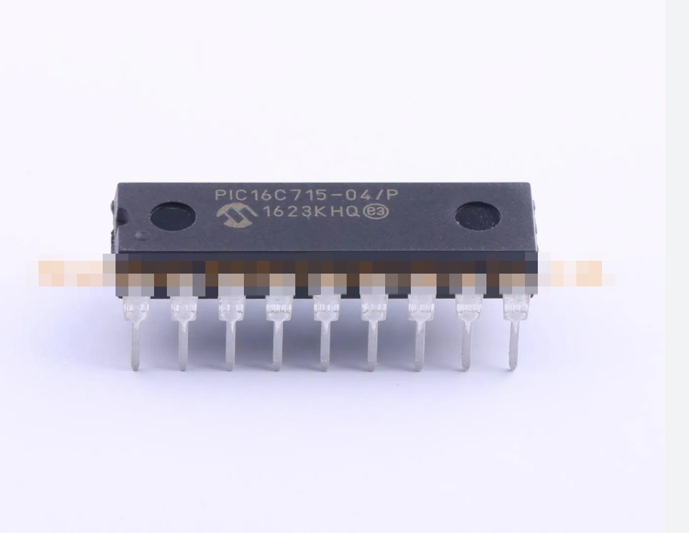
The PIC16C715 is a classic 8‑bit microcontroller from Microchip’s mid‑range family, built around embedded EPROM technology. Unlike modern flash devices, this chip is one‑time programmable (OTP) – meaning its memory can be written exactly once. It features 3.5KB of program memory, 128 bytes of EEPROM‑like data storage, and a built‑in 4‑channel 8‑bit ADC. Due to its high reliability and low cost, the PIC16C715 was widely deployed in automotive keyless entry systems, industrial sensor interfaces, medical infusion pumps, and consumer appliance controllers. Many manufacturers set protective lock bits to secure the binary file inside, turning the microcontroller into a locked black box. When the original source code is lost or the device becomes obsolete, the only archive of the firmware remains trapped in the protected memory. Recovering that data is critical to avoid scrapping expensive equipment.
PORTB is an 8-bit wide bi-directional port. The corresponding data direction register is TRISB. Setting a bit in the TRISB register puts the corresponding output driver in a hi-impedance input mode when Attack MCU PIC16C715 Software. Clearing a bit in the TRISB register puts the contents of the output latch on the selected pin(s).
Each of the PORTB pins has a weak internal pull-up. A single control bit can turn on all the pull-ups. This is performed by clearing bit RBPU (OPTION<7>). The weak pull-up is automatically turned off when the port pin is configured as an output. The pull-ups are disabled on a Power-on Reset.
Four of PORTB’s pins, RB7:RB4, have an interrupt on change feature. Only pins configured as inputs can cause this interrupt to occur (i.e. any RB7:RB4 pin configured as an output is excluded from the interrupt on change comparison).
To attack a locked PIC16C715, standard programmers are useless because the protective encrypted lock bits completely block any readout of the program memory. Our service employs specialised invasive techniques tailored for OTP chips. First, we decapsulate the plastic package using precise chemical etching to expose the silicon die. Then, we hack into the memory array by probing the data buses or exploiting the EPROM cell characteristics. The goal is to decode the binary program – a heximal file that represents the original source code logic. Once we retrieve the firmware, we can clone or duplicate it into a fresh microcontroller (such as a compatible flash‑based PIC or an exact OTP replacement). This break process is non‑destructive to the data itself, preserving the archive integrity. Unlike flash chips, OTP devices like the PIC16C715 require careful handling because the memory cannot be erased or rewritten, making our decapsulate and retrieve method the only viable solution.
The input pins (of RB7:RB4) are compared with the old value latched on the last attack of PORTB. The “mismatch” outputs of RB7:RB4 are OR’ed together to generate the RB Port Change Interrupt with flag bit RBIF (INTCON<0>).
Any instruction which writes, operates internally as a attack followed by a write operation. The BCF and BSF instructions, for example, attack the register into the CPU, execute the bit operation and write the result back to the register to ease the process of Attack MCU PIC16C715 Software. Caution must be used when these instructions are applied to a port with both inputs and outputs defined.
For example, a BSF operation on bit5 of PORTB will cause all eight bits of PORTB to be attack into the CPU. Then the BSF operation takes place on bit5 and PORTB is written to the output latches.
If another bit of PORTB is used as a bi-directional I/O pin (e.g., bit0) and it is defined as an input at this time, the input signal present on the pin itself would be attack into the CPU and rewritten to the data latch of this particular pin, overwriting the previous content. As long as the pin stays in the input mode, no problem occurs. However, if bit0 is switched to an output, the content of the data latch may now be unknown.
The demand to attack and recover firmware from secured PIC16C715 microcontrollers comes from urgent industrial needs. First, obsolete automation lines: many factory sensors and controllers still run on this chip, but the original heximal file was lost when a supplier closed. Second, medical device maintenance: infusion pumps and diagnostic tools using the PIC16C715 cannot be cloned without decoding the locked program. Third, automotive electronics: keyless entry modules with protected memory fail over time, and manufacturers no longer provide replacement chips. By performing a clean retrieve and duplicate of the binary archive, we enable clients to clone the firmware into new microcontrollers – avoiding costly system redesigns. The benefits are tangible: extended product lifecycle, reduced e‑waste, and preserved intellectual property without needing the original source code.
The actual write to an I/O port happens at the end of an instruction cycle, whereas for attacking, the data must be valid at the beginning of the instruction cycle. Therefore, care must be exercised if a write followed by a attack operation is carried out on the same I/O port. The sequence of instructions should be such to allow the pin voltage to stabilize (load dependent) before the next instruction which causes that file to be attack into the CPU is executed. Otherwise, the previous state of that pin may be attack into the CPU rather than the new state. When in doubt, it is better to separate these instructions with a NOP or another instruction not accessing this I/O port.
We offer confidential, fast, and precise attack services for the PIC16C715 and many other OTP microcontrollers. Every break procedure is performed with care to preserve data integrity. Contact us with your locked chip, and we will decapsulate, decode, and retrieve the complete binary or heximal file – turning a protective memory into a usable archive for production, cloning, or reverse engineering.