 Copy Microcontroller PIC16F627A Binary
 August 22nd, 2014 |
  Author:
 We can Copy Microcontroller PIC16F627A Binary, please view the Microcontroller PIC16F627A features for your reference:
High Performance RISC CPU:
Operating speeds from DC – 20 MHz
Interrupt capability
Direct, Indirect and Relative Addressing modes
35 single word instructions
– All instructions single cycle except branches
Special Microcontroller Features:
· Internal and external oscillator options
– Precision Internal 4 MHz oscillator factory calibrated to ±1%
– Low Power Internal 37 kHz oscillator
– External Oscillator support for crystals and resonators
· Power saving SLEEP mode
· Programmable weak pull-ups on PORTB
· Multiplexed Master Clear/Input-pin
· Watchdog Timer with independent oscillator for reliable operation
· Low voltage programming
· In-Circuit Serial Programming™ (via two pins)
· Programmable code protection
· Brown-out Reset
· Power-on Reset
· Power-up Timer and Oscillator Start-up Timer
· Wide operating voltage range. (2.0 – 5.5V)
· Industrial and extended temperature range
· High Endurance FLASH/EEPROM Cell
– 100,000 write FLASH endurance
– 1,000,000 write EEPROM endurance
Low Power Features:
· Standby Current:
– 100 nA @ 2.0V, typical
· Operating Current:
– 12 µA @ 32 kHz, 2.0V, typical
– 120 µA @ 1 MHz, 2.0V, typical
· Watchdog Timer Current
– 1 µA @ 2.0V, typical
· Timer1 oscillator current:
– 1.2 µA @ 32 kHz, 2.0V, typical
· Dual Speed Internal Oscillator:
– Run-time selectable between 4 MHz and 37 kHz
– 4 µs wake-up from SLEEP, 3.0V, typical
Peripheral Features:
· 16 I/O pins with individual direction control
· High current sink/source for direct LED drive
· Analog comparator module with:
– Two analog comparators
– Programmable on-chip voltage reference (VREF) module
– Selectable internal or external reference
– Comparator outputs are externally accessible
· Timer0: 8-bit timer/counter with 8-bit programmable prescaler
· Timer1: 16-bit timer/counter with external crystal/clock capability
· Timer2: 8-bit timer/counter with 8-bit period register, prescaler and postscaler
· Capture, Compare, PWM module
– 16-bit Capture/Compare
– 10-bit PWM
· Addressable Universal Synchronous/Asynchronous Receiver/Transmitter USART/SCI
 Posted in
Attack IC PIC16C74B Binary
Depending on application and production requirements, the proper device option can be selected using the information in the PIC16C74B Product Identification System section at the end of this data sheet which can help to ease the process of Attack IC PIC16C74B Binary.
For the PIC16C7X family, there are two device “types” as indicated in the device number:
1. C, as in PIC16C74. These devices have EPROM type memory and operate over the standard voltage range.
2. LC, as in PIC16LC74. These devices have EPROM type memory and operate over an extended voltage range.
The UV erasable version, offered in windowed CERDIP packages, is optimal for prototype development and pilot programs. This version can be erased and reprogrammed to any of the oscillator modes. The availability of OTP devices is especially useful for customers who need the flexibility for frequent code updates and small volume applications.
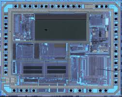
Attack IC PIC16C74B Binary
The OTP devices, packaged in plastic packages, permit the user to program them once. In addition to the program memory, the configuration bits must also be programmed.
Microchip offers a QTP Programming Service for factory production orders. This service is made available for users who choose not to program a medium to high quantity of units and whose code patterns have stabilized to prohibit the operation of Attack IC PIC16C74B Binary. The devices are identical to the OTP devices but with all EPROM locations and configuration options already programmed by the factory.
The high performance of the PIC16CXX family can be attributed to a number of architectural features commonly found in RISC microprocessors. To begin with, the PIC16CXX uses a Harvard architecture, in which program and data are accessed from separate memories using separate buses.
This improves bandwidth over traditional von Neumann architecture, in which program and data are fetched from the same memory using the same bus. Separating program and data buses further allows instructions to be sized differently than the 8-bit wide data word. Instruction opcodes are 14-bits wide, making it possible to have all single word instructions. A 14-bit wide program memory access bus fetches a 14-bit instruction in a single cycle.
A two-stage pipeline overlaps fetch and execution of instructions (Example 3-1). Consequently, most instructions execute in a single cycle (200 ns @ 20 MHz) except for program branches. All devices covered by this data sheet contain 4K x 14-bit program memory and 192 x 8-bit data memory.
Copy IC PIC16F884 Code
Copy IC PIC16F884 Code is covered by this data sheet. The PIC16F884 is available in 28-pin PDIP, SOIC, SSOP and QFN packages. The PIC16F884/887 is available in a 40-pin PDIP and 44-pin QFN and TQFP packages when Copy IC. Figure 1-1 shows the block diagram of PIC16F884 and Figure 1-2 shows a block diagram of the PIC16F884 device.
Table 1-1 and Table 1-2 show the corresponding pinout descriptions. The PIC16F884 has a 13-bit program counter capable of addressing a 2K x 14 (0000h-07FFh) for the PIC16F882, 4K x 14 (0000h-0FFFh) for the PIC16F883/PIC16F884, and 8K x 14 (0000h-1FFFh) for the PIC16F884 program memory space.
Accessing a location above these boundaries will cause a wrap-around within the first 8K x 14 space. The Reset vector is at 0000h and the interrupt vector is at 0004h.
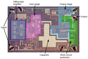
Copy IC PIC16F884 Code
The data memory is partitioned into four banks which contain the General Purpose Registers (GPR) and the Special Function Registers (SFR). The Special Function Registers are located in the first 32 locations of each bank. The General Purpose Registers, implemented as static RAM, are located in the last 96 locations of each Bank.
Register locations F0h-FFh in Bank 1, 170h-17Fh in Bank 2 and 1F0h-1FFh in Bank 3, point to addresses 70h-7Fh in Bank 0. The actual number of General Purpose Resisters (GPR) implemented in each Bank depends on the device when Copy IC PIC16F884 Code. Details are shown in Figures 2-5 and 2-6. All other RAM is unimplemented and returns ‘0’ when read. RP<1:0> of the STATUS register are the bank select bits:
RP1 RP0
→Bank 0 is selected
→Bank 1 is selected
→Bank 2 is selected
→Bank 3 is selected
Circuit Engineering Company Limited continues to be recognized as the Southern China Leader in Services for IC Read, MCU Crack, Chip Copy, Microcontroller Unlock service. With the advancement of today’s modern circuit board technology, it is more important than ever to have specialists available to help you at a moment’s notice. Our engineering and commercial teams collectively have a vast amount of electronic experience covering field include Consumer Electronics, Industrial Automation Electronics, Wireless Communication Electronics., etc. For more information please contact us through email.
Copy Microcontroller PIC18F4515 Code
Like previous PIC18 devices, Copy Microcontroller PIC18F4515 Code includes a feature that allows the device clock source to be switched from the main oscillator to an alternate low-frequency clock source. PIC18F2X1X/4X1X devices offer two alternate clock sources.
When an alternate clock source is enabled, the various power managed operating modes are available. Essentially, there are three clock sources for these devices:
· Primary oscillators
· Secondary oscillators
· Internal oscillator block
The primary oscillators include the External Crystal and Resonator modes, the External RC modes, the External Clock modes and the internal oscillator block. The particular mode is defined by the FOSC3:FOSC0 configuration bits. The details of these modes are covered earlier in this chapter.
The secondary oscillators are those external sources not connected to the OSC1 or OSC2 pins. These sources may continue to operate even after the controller is placed in a power managed mode. PIC18F2X1X/4X1X devices offer the Timer1 oscillator as a secondary oscillator which will bring more difficult in the process of Copy Microcontroller PIC18F4515 Code. This oscillator, in all power managed modes, is often the time base for functions such as a real-time clock.
Most often, a 32.768 kHz watch crystal is connected between the RC0/T1OSO/T13CKI and RC1/T1OSI pins. Like the LP mode oscillator circuit, loading capacitors are also connected from each pin to ground. The Timer1 oscillator is discussed in greater detail in Section 11.3 “Timer1 Oscillator”.
In addition to being a primary clock source, the internal oscillator block is available as a power managed mode clock source. The INTRC source is also used as the clock source for several special features, such as the WDT and Fail-Safe Clock Monitor.
The clock sources for the PIC18F2X1X/4X1X devices are shown in Figure 2-8. See Section 22.0 “Special Features of the CPU” for Configuration register details. The OSCCON register (Register 2-2) controls several aspects of the device clock’s operation, both in full power operation and in power managed modes.
The System Clock Select bits, SCS1:SCS0, select the clock source. The available clock sources are the primary clock (defined by the FOSC3:FOSC0 configuration bits), the secondary clock (Timer1 oscillator) and the internal oscillator block. The clock source changes immediately after one or more of the bits is written to, following a brief clock transition interval.
Copy IC PIC12C671 Eeprom
We can Copy IC PIC12C671 Eeprom, please view the IC PIC12C671 features for your reference:
High-Performance RISC CPU:
· Only 35 single word instructions to learn
· All instructions are single cycle (400 ns) except for program branches which are two-cycle
· Operating speed: DC – 10 MHz clock input DC – 400 ns instruction cycle
· 14-bit wide instructions 8-bit wide data path
· Interrupt capability
· Special function hardware registers
· 8-level deep hardware stack
· Direct, indirect and relative addressing modes for data and instructions
Peripheral Features:
· Four-channel, 8-bit A/D converter
· 8-bit real time clock/counter (TMR0) with 8-bit programmable prescaler
· 1,000,000 erase/write cycle EEPROM data memory
· EEPROM data retention > 40 years
Special Microcontroller Features:
In-Circuit Serial Programming (ICSP™)
Internal 4 MHz oscillator with programmable calibration
Selectable clockout
Power-on Reset (POR)
Power-up Timer (PWRT) and Oscillator Start-up
Timer (OST)
Copy IC PIC12C671 Eeprom
Watchdog Timer (WDT) with its own on-chip RC oscillator for reliable operation and facilitate the operation of Copy IC PIC12C671 Eeprom
Power saving SLEEP mode
Interrupt-on-pin change (GP0, GP1, GP3)
Internal pull-ups on I/O pins (GP0, GP1, GP3)
Internal pull-up on MCLR pin
Selectable oscillator options:
– INTRC: Precision internal 4 MHz oscillator
– EXTRC: External low-cost RC oscillator
– XT: Standard crystal/resonator
– HS: High speed crystal/resonator
– LP: Power saving, low frequency crystal
CMOS Technology:
· Low-power, high-speed CMOS EPROM/EEPROM technology
· Fully static design
· Wide operating voltage range 2.5V to 5.5V
· Commercial, Industrial and Extended temperature ranges
· Low power consumption
< 2 mA @ 5V, 4 MHz
15 µA typical @ 3V, 32 kHz
< 1 µA typical standby current
Copy Microcontroller PIC18F4220 Binary
Memory Endurance: The Enhanced Flash cells for both program memory and data EEPROM are rated to last for many thousands of erase/write cycles – up to 100,000 for program memory and 1,000,000 for EEPROM which has provide a preferential terms for Copy Microcontroller PIC18F4220 Binary. Data retention without refresh is conservatively estimated to be greater than 40 years.
· Self-programmability: These devices can write to their own program memory spaces under internal software control. By using a bootloader routine located in the protected Boot Block at the top of program memory, it becomes possible to create an application that can update itself in the field.
· Enhanced CCP Module: In PWM mode, this module provides 1, 2 or 4 modulated outputs for controlling half-bridge and full-bridge drivers. Other features include Auto-Shutdown for disabling PWM outputs on interrupt or other select conditions and Auto-Restart to reactivate outputs once the condition has cleared.
Addressable USART: This serial communication module is capable of standard RS-232 operation using the internal oscillator block, removing the need for an external crystal (and its accompanying power requirement) in applications that talk to the outside world.
· 10-bit A/D Converter: This module incorporates programmable acquisition time, allowing for a channel to be selected and a conversion to be initiated without waiting for a sampling period and thus, reduce code overhead.
· Extended Watchdog Timer (WDT): This enhanced version incorporates a 16-bit prescaler, allowing a time-out range from 4 ms to over 2 minutes, that is stable across operating voltage and temperature.
The EC and ECIO Oscillator modes require an external clock source to be connected to the OSC1 pin. There is no oscillator start-up time required after a Power-on Reset or after an exit from Sleep mode after Copy Microcontroller PIC18F4220 Binary.
In the EC Oscillator mode, the oscillator frequency divided by 4 is available on the OSC2 pin. This signal may be used for test purposes or to synchronize other logic. Figure 2-4 shows the pin connections for the EC Oscillator mode.
For timing insensitive applications, the “RC” and “RCIO” device options offer additional cost savings. The RC oscillator frequency is a function of the supply voltage, the resistor (REXT) and capacitor (CEXT) values and the operating temperature.
In addition to this, the oscillator frequency will vary from unit to unit due to normal manufacturing variation. Furthermore, the difference in lead frame capacitance between package types will also affect the oscillation frequency, especially for low CEXT values.
The user also needs to take into account variation due to tolerance of external R and C components used. Figure 2-6 shows how the R/C combination is connected. In the RC Oscillator mode, the oscillator frequency divided by 4 is available on the OSC2 pin. This signal may be used for test purposes or to synchronize other logic.
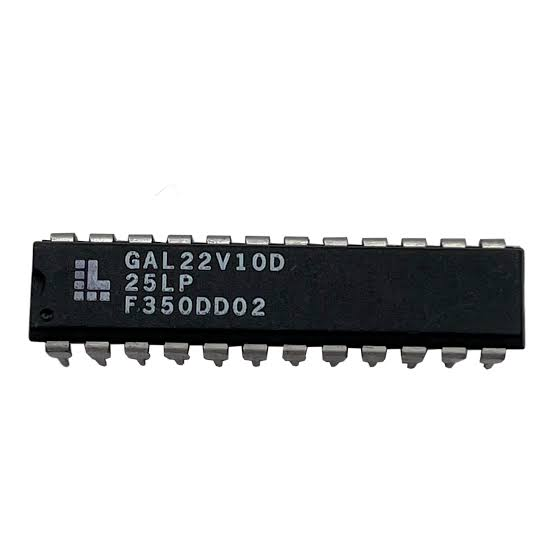
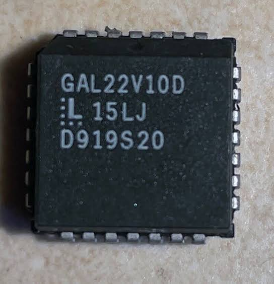
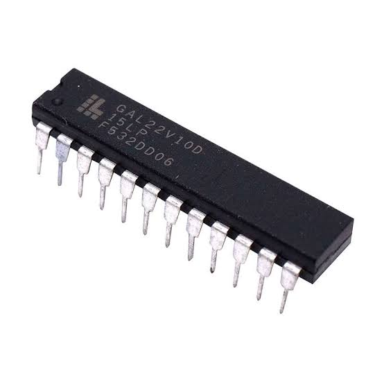
Break IC GAL22V10D-10LJ Binary
The GAL22V10D-10LJ is a classic Programmable Logic Device (PLD) from Lattice Semiconductor, widely deployed in automotive engine control units, industrial automation controllers, telecommunications infrastructure, medical instrumentation, and military avionics. Unlike a standard microcontroller, this chip contains a embedded logic array that implements custom firmware – typically in the form of binary logic equations rather than source code.
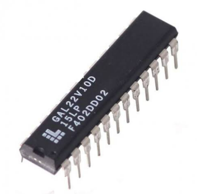
Its key features include 10 macrocells, 22 inputs, high-speed operation (10 ns propagation delay), and a protective security fuse that, when locked, prevents any readout of the internal data. Many legacy systems still rely on this PLD because of its reliability and low power consumption. However, when the original design file or heximal program is lost, the secured memory becomes an inaccessible archive that threatens the entire product’s maintainability.

Break IC GAL22V10D-10LJ Binary from its memory and rewrite the program into new PLD GAL22V10D:
HIGH PERFORMANCE E2CMOS® TECHNOLOGY
— 4 ns Maximum Propagation Delay
— Fmax = 250 MHz
— 3.5 ns Maximum from Clock Input to Data Output
— UltraMOS® Advanced CMOS Technology which has been fully developed in the process of Break IC GAL22V10D-10LJ Binary
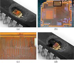
The need to break into a locked GAL22V10D arises when equipment becomes obsolete and the original source code or binary file no longer exists. Without the ability to retrieve the internal firmware, a failed chip would scrap expensive machinery. To hack this PLD, one must first decapsulate the plastic package using chemical or laser techniques, then physically probe the embedded memory cells or exploit timing faults to decode the encrypted logic pattern. The goal is to clone or duplicate the exact program into a new device. The protective security fuse on the GAL22V10D is designed to block standard programmers from performing a readout. Thus, a direct attack is impossible without invasive methods. Our service specializes in this break process:
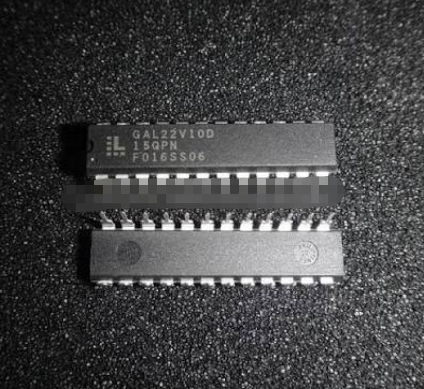
we decapsulate the chip, retrieve the binary data from the flash-equivalent cells, and produce a complete heximal file that mirrors the original firmware. This archive can then be cloned into fresh PLD units, restoring full functionality.
· ACTIVE PULL-UPS ON ALL PINS
· COMPATIBLE WITH STANDARD 22V10 DEVICES
— Fully Function/Fuse-Map/Parametric Compatible with Bipolar and UVCMOS 22V10 Devices
· 50% to 75% REDUCTION IN POWER VERSUS BIPOLAR
— 90mA Typical Icc on Low Power Device
— 45mA Typical Icc on Quarter Power Device
· E2 CELL TECHNOLOGY
— Reconfigurable Logic
— Reprogrammable Cells
— 100% Tested/100% Yields
— High Speed Electrical Erasure (<100ms)
— 20 Year Data Retention
· TEN OUTPUT LOGIC MACROCELLS
— Maximum Flexibility for Complex Logic Designs
Our break procedure follows a disciplined workflow. First, we chemically decapsulate the protected GAL22V10D without damaging the silicon die. Next, using micro‑probing stations, we decode the locked logic configuration stored in the EEPROM‑like cells. The extracted binary is then verified against the original chip’s behavior. Finally, we deliver a heximal file that can be programmed into any compatible PLD – effectively allowing you to clone or duplicate the program for unlimited replacements. The benefits for our clients are substantial: you avoid costly system redesigns, extend the life of obsolete equipment, and regain control over your embedded firmware. Whether you need to retrieve a lost archive, clone a failing chip, or simply decode a secured logic pattern for reverse engineering, our service delivers a clean, reliable binary output.
· PRELOAD AND POWER-ON RESET OF REGISTERS
— 100% Functional Testability
· APPLICATIONS INCLUDE:
— DMA Control
— State Machine Control
— High Speed Graphics Processing
— Standard Logic Speed Upgrade
· ELECTRONIC SIGNATURE FOR IDENTIFICATION
The GAL22V10, at 4ns maximum propagation delay time, combines a high performance CMOS process with Electrically Erasable (E2) floating gate technology to provide the highest performance available of any 22V10 device on the market.
CMOS circuitry allows the GAL22V10 to consume much less power when compared to bipolar 22V10 devices. E2 technology offers high speed (<100ms) erase times, providing the ability to reprogram or reconfigure the device quickly and efficiently which is critical for Break IC GAL22V10D-10LJ Binary.
The generic architecture provides maximum design flexibility by allowing the Output Logic Macrocell (OLMC) to be configured by the user. The GAL22V10 is fully function/fuse map/parametric compatible with standard bipolar and CMOS 22V10 devices.
Unique test circuitry and reprogrammable cells allow complete AC, DC, and functional testing during manufacture. As a result, Lattice Semiconductor delivers 100% field programmability and functionality of all GAL products. In addition, 100 erase/write cycles and data retention in excess of 20 years are specified.
We offer confidential, fast, and precise break services for the GAL22V10D-10LJ and many other PLD families. Every attack is performed with care to preserve the data integrity. Contact us with your locked chip, and we will decapsulate, decode, and retrieve the complete binary file – turning a protected memory into a usable archive for production.
Break Microcontroller MSP430F4361 Software
Break Microcontroller MSP430F4361 Software
MSP430 Microcontrollers (MCUs) from Texas Instruments (TI) are 16-bit, RISC-based, mixed-signal processors designed specifically for ultra-low-power. MSP430 MCUs have the right mix of intelligent peripherals, ease-of-use, low cost and lowest power consumption for thousands of applications which makes it becomes popular to Break Microcontroller MSP430F4361 Software.
TI offers robust design support for the MSP430 MCU platform along with technical documents, training, tools and software to help designers develop products and release them to market faster.
MSP430 Microcontroller DNA
Ultra-Low Power
The MSP430 MCU is designed specifically for ultra-low-power applications. Its flexible clocking system, multiple low-power modes, instant wakeup and intelligent autonomous peripherals enable true ultra-low-power optimization, dramatically extending battery life.
Flexible Clocking System – The MSP430 MCU clock system has the ability to enable and disable various clocks and oscillators which allow the device to enter various low-power modes (LPMs). The flexible clocking system optimizes overall current consumption by only enabling the required clocks when appropriate.
Multiple-Oscillator Clock System
Key Features
· Integrated intelligent peripherals including a wide range of high-performance analog and digital peripherals that off-load the CPU
· Easy-to-use 16-bit RISC CPU architecture enables new applications with industry-leading code density.
· Complete development ecosystem with tools starting at $4.30
400+ Ultra-Low-Power Devices
8-MHz to 25-MHz CPU Speed
0.5KB to 256KB Flash
128B to 18KB RAM
14 to 113 pins; 25+ packages
Sub-Main Clock (SMCLK) – Source for faster individual peripheral modules that may be driven by the internal DCO up to 25 MHz or with external crystal.
Instant Wakeup – The MSP430 MCU can wake-up instantly from LPMs. This ultra-fast wake-up is enabled by the MSP430 MCU’s internal digitally controlled oscillator (DCO), which can source up to 25 MHz and be active and stable in 1µs. Instant wake-up functionality is important in ultra-low-power applications since it allows the microcontroller to use the CPU in very efficient bursts and spend more time in LPMs and provide a better chance to Break Microcontroller MSP430F4361 Software.
Zero-Power Brown-Out Reset (BOR) – The MSP430 MCU’s BOR is always enabled and active in all modes of operation.
the most reliable performance possible while maintaining ultra-low-power consumption. The BOR circuit detects low supply voltages and Lower-Power Peripherals resets the device when power is applied or removed. This functionality is especially critical in battery-powered applications.
Recover IC PIC16C74 Code
A variety of frequency ranges and packaging options are available when Recover IC PIC16C74 Code. Depending on application and production requirements, the proper device option can be selected using the information in the PIC16C7X Product Identification System section at the end of this data sheet.
When placing orders, please use that page of the data sheet to specify the correct part number.
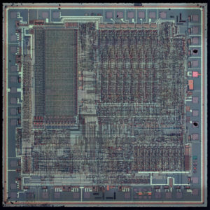
Recover IC PIC16C74 Code
For the PIC16C7X family, there are two device “types” as indicated in the device number:
1. C, as in PIC16C74. These devices have EPROM type memory and operate over the standard voltage range.
2. LC, as in PIC16LC74. These devices have EPROM type memory and operate over an extended voltage range.
The UV erasable version, offered in CERDIP package is optimal for prototype development and pilot programs. This version can be erased and reprogrammed to any of the oscillator modes to Recover IC PIC16C74 Code. Microchip’s PICSTART® Plus and PRO MATE® II programmers both support programming of the PIC16C7X.
The OTP devices, packaged in plastic packages, permit the user to program them once. In addition to the program memory, the configuration bits must also be programmed.
Microchip offers a QTP Programming Service for factory production orders. This service is made available for users who choose not to program a medium to high quantity of units and whose code patterns have stabilized. The devices are identical to the OTP devices but with all EPROM locations and configuration options already programmed by the factory.
Microchip offers a unique programming service where a few user-defined locations in each device are programmed with different serial numbers. The serial numbers may be random, pseudo-random, or sequential. Serial programming allows each device to have a unique number which can serve as an entry-code, password, or ID number.
Copy MCU PIC16C72 Software
We can Copy MCU PIC16C72 Software, please see the MCU PIC16C72 features for your reference:
PIC16C7X Microcontroller Core Features:
· High-performance RISC CPU
· Only 35 single word instructions to learn
· All single cycle instructions except for program branches which are two cycle
· Operating speed: DC – 20 MHz clock input DC – 200 ns instruction cycle
· Up to 8K x 14 words of Program Memory, up to 368 x 8 bytes of Data Memory (RAM)
· Interrupt capability
· Eight level deep hardware stack
· Direct, indirect, and relative addressing modes
· Power-on Reset (POR)
Copy MCU PIC16C72 Software
· Power-up Timer (PWRT) and Oscillator Start-up Timer (OST)
· Watchdog Timer (WDT) with its own on-chip RC oscillator for reliable operation
· Programmable code-protection
· Power saving SLEEP mode
· Selectable oscillator options
· Low-power, high-speed CMOS EPROM technology
· Fully static design
· Wide operating voltage range: 2.5V to 6.0V
· High Sink/Source Current 25/25 mA
· Commercial, Industrial and Extended temperature ranges
· Low-power consumption:
· < 2 mA @ 5V, 4 MHz
· 15 µA typical @ 3V, 32 kHz
· < 1 µA typical standby current
PIC16C7X Peripheral Features:
· Timer0: 8-bit timer/counter with 8-bit prescaler
· Timer1: 16-bit timer/counter with prescaler, can be incremented during sleep via external crystal/clock
· Timer2: 8-bit timer/counter with 8-bit period register, prescaler and postscaler
· Capture, Compare, PWM module(s)
· Capture is 16-bit, max. resolution is 12.5 ns, Compare is 16-bit, max. resolution is 200 ns, PWM max. resolution is 10-bit from Copy MCU PIC16C72 Software
· 8-bit multichannel analog-to-digital converter
· Synchronous Serial Port (SSP) with SPI and I2C
· Universal Synchronous Asynchronous Receiver Transmitter (USART/SCI)
· Parallel Slave Port (PSP) 8-bits wide, with external RD, WR and CS controls
· Brown-out detection circuitry for Brown-out Reset (BOR)