 Copy Microcontroller PIC16F767 Program
 November 3rd, 2010 |
  Author:
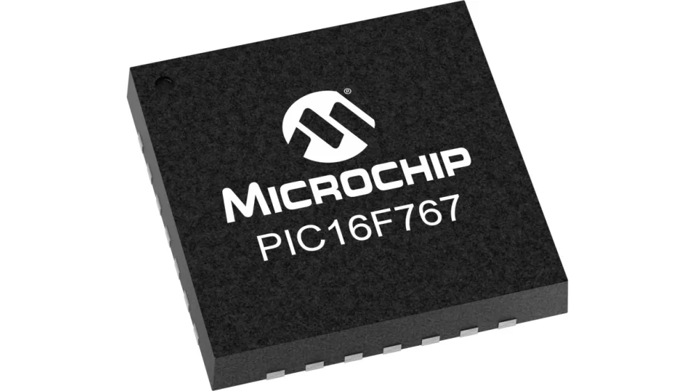
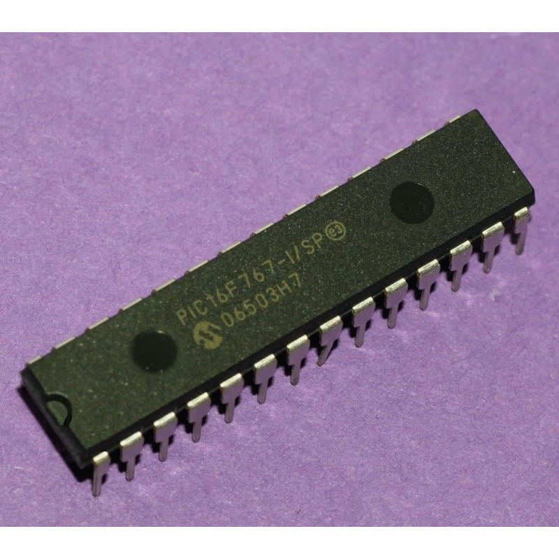
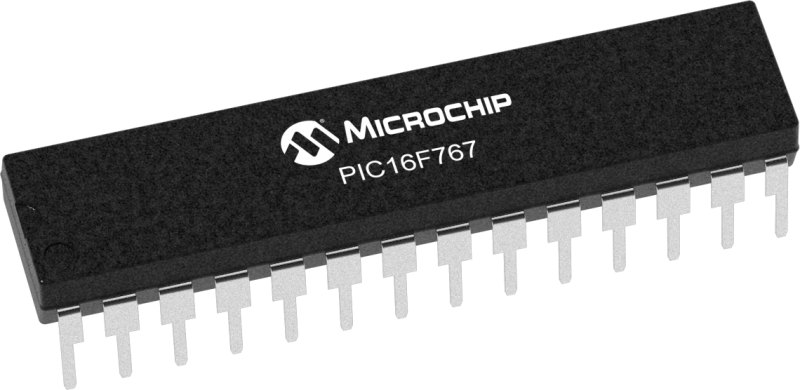
 The PIC16F767 is a highly sophisticated 28-pin MCU that has become a cornerstone in mid-range industrial and commercial applications. Known for its integrated analog-to-digital converters, multiple timers, and nanoWatt technology for low power consumption, this chip is frequently found in medical respiratory equipment, advanced HVAC control systems, and high-precision weighing scales. Its unique architecture provides a generous flash memory and an internal eeprom for non-volatile data storage, allowing for complex program routines in a compact package. However, many of these embedded systems are deployed with protective locks to safeguard intellectual property. When a legacy board fails or the original source code is lost, the locked or secured state of the chip makes traditional troubleshooting impossible, leaving the protected logic trapped within the silicon.
MEMORY ORGANIZATION
There are two memory blocks in each of these PICmicro® MCUs. The program memory and data memory have separate buses so that concurrent access can occur and is detailed in this section. The program memory can be read internally by user code (see Section 3.0 “Reading Program Memory”). Additional information on device memory may be found in the “PICmicro® Mid-Range MCU Family Reference Manual” (DS33023). The PIC16F767 devices have a 13-bit program counter capable of addressing an 8K word x 14-bit program memory space. The PIC16F767 devices have 8K words of Flash program memory and the PIC16F767 devices have 4K words. The program memory maps for PIC16F7X7 devices are shown in Figure 2-1. Accessing a location above the physically implemented address will cause a wraparound. in the “PICmicro® Mid-Range MCU Family Reference.
The Reset vector is at 0000h and the interrupt vector is at 0004h. The data memory is partitioned into multiple banks which contain the General Purpose Registers and the Special Function Registers. Bits RP1 (Status<6>) and RP0 (Status<5>) are the bank select bits. Each bank extends up to 7Fh (128 bytes). The lower locations of each bank are reserved for the Special Function Registers. Above the Special Function Registers are General Purpose Registers, implemented as static RAM. All implemented banks contain Special Function Registers. Some frequently used Special Function Registers from one bank may be mirrored in another bank for code reduction and quicker access.
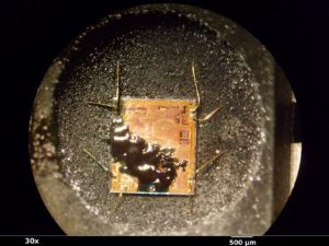
Our specialized laboratory offers a high-level technical service to break through these hardware-level restrictions and retrieve the critical binary archive necessary for system continuity. To successfully attack a secured MCU, our engineers employ advanced laboratory techniques to decapsulate the physical housing, allowing direct access to the internal circuitry for micro-probing and analysis. This process enables us to decode the heximal data directly from the protected memory layers without damaging the underlying logic. Whether the goal is to clone an obsolete controller to keep a production line running or to duplicate the firmware from a locked device for disaster recovery, our service provides a reliable pathway to hack the physical and logical barriers of the embedded chip. By extracting the binary file with 100% integrity, we transform a secured component back into a functional, portable program archive.
The primary purpose of performing a targeted attack to break the security of a protected PIC16F767 is to avoid the devastating costs of forced hardware obsolescence. For many end users, the ability to retrieve a heximal archive from a locked MCU is a strategic necessity that protects decades of investment in specialized machinery. By choosing to decode or hack the secured architecture of an existing chip, organizations can clone or duplicate their vital firmware onto replacement hardware, bypassing the need for a costly ground-up redesign. Our expertise allows you to duplicate the flash and eeprom data from any embedded controller, ensuring that the binary logic is preserved and ready for deployment. This service turns a locked or encrypted “black box” into a manageable and secure source code asset for your maintenance team.
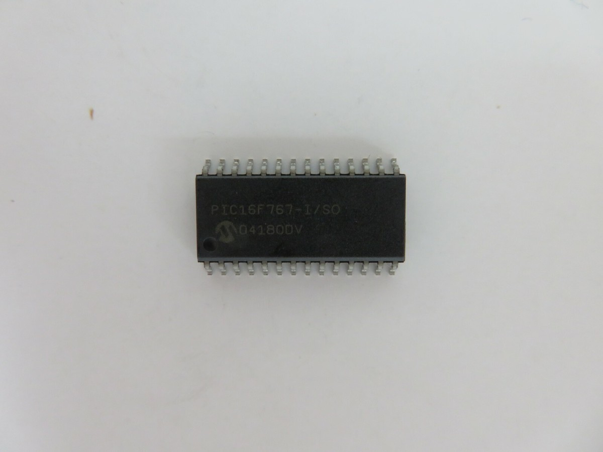
Ultimately, our recovery service provides the end user with total autonomy over their hardware maintenance and software lifecycle. Instead of facing the impossible task of recreating lost program logic, you can simply retrieve the heximal file and clone the locked data directly onto a fresh MCU. We specialize in the precision required to decapsulate and attack these high-security components, ensuring that the binary data is handled with surgical accuracy. By providing a reliable way to decode and duplicate the firmware of a secured PIC16F767, we turn a protected archive into a functional reality once again. Our commitment is to ensure that your data, memory, and program files remain accessible, regardless of the protective measures originally placed upon the silicon, ensuring your systems remain operational for years to come.
Copy Microcontroller PIC16F747 Code
The PIC16F747 is a powerful embedded MCU featuring 7 KB of flash memory, 256 bytes of eeprom, and a 10-bit ADC, making it a cornerstone in automotive dashboards, industrial pumps, HVAC controllers, and medical monitoring devices. Its protected architecture includes locked configuration bits and encrypted readout protection, designed to safeguard proprietary source code.
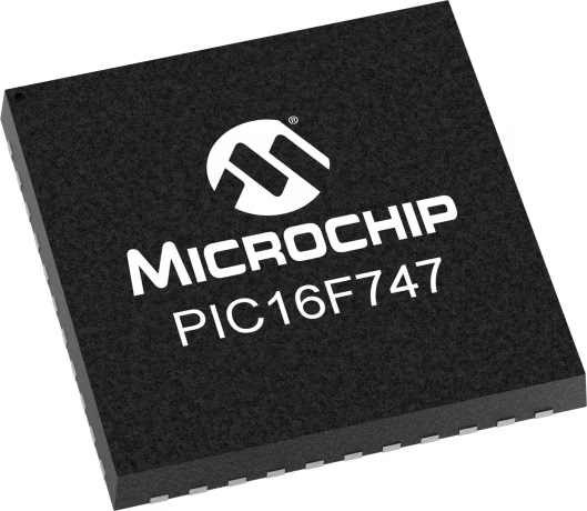
Yet when original binary files are lost due to outdated programming tools or supplier bankruptcy, engineers need legitimate ways to duplicate the chip’s logic. Unlike simpler 8-bit cousins, the PIC16F747 uses a complex interrupt vector table and internal oscillator calibration values stored in protected memory – losing these means replacing whole systems. Our service specializes in ethical clone operations: we retrieve every data byte from the secured die, enabling production continuity without redesigning the entire PCB.
Special Microcontroller Features:
· Fail-Safe Clock Monitor for protecting critical applications against crystal failure;
· Two-Speed Start-up mode for immediate code execution
· Power-on Reset (POR), Power-up Timer (PWRT) and Oscillator Start-up Timer (OST)
· Programmable Code Protection
· Processor Read Access to Program Memory
· Power-Saving Sleep mode
· In-Circuit Serial Programming (ICSP) via two pins
· MPLAB® In-Circuit Debug (ICD) via two pins
· MCLR pin function replaceable with input only pin
DEVICE OVERVIEW
This document contains device specific information about the following devices:
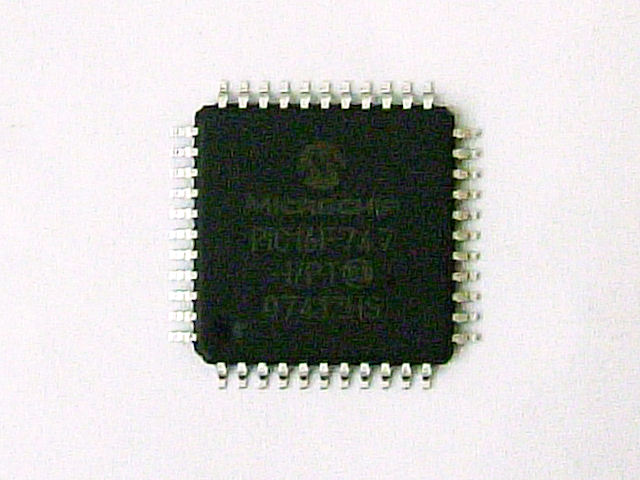
PIC16F737/767 devices are available only in 28-pin packages, while PIC16F747/777 devices are available in 40-pin and 44-pin packages. All devices in the PIC16F7X7 family share common architecture with the following differences:
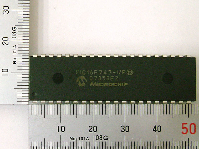
· The PIC16F737 and PIC16F767 have one-half of the total on-chip memory of the PIC16F747 and PIC16F777.
· The 28-pin devices have 3 I/O ports, while the 40/44-pin devices have 5.
· The 28-pin devices have 16 interrupts, while the 40/44-pin devices have 17.
· The 28-pin devices have 11 A/D input channels, while the 40/44-pin devices have 14.
· The Parallel Slave Port is implemented only on the 40/44-pin devices.
· Low-Power modes: RC_RUN allows the core and peripherals to be clocked from the INTRC, while SEC_RUN allows the core and peripherals to be clocked from the low-power Timer1. Refer to
Section 4.7 “Power-Managed Modes” for further details.
· Internal RC oscillator with eight selectable frequencies, including 31.25 kHz, 125 kHz, 250 kHz, 500 kHz, 1 MHz, 2 MHz, 4 MHz and 8 MHz. The INTRC can be configured as a primary or secondary clock source. Refer to Section 4.5 “Internal Oscillator Block” for further details.
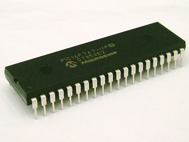
To break into a locked PIC16F747, the first step is decapsulate the epoxy using acid or laser etching, exposing the silicon die. Then, specialists apply fault injection or side-channel analysis to attack the protective readout guard. This non-destructive method reveals the heximal (Intel HEX) program stored in flash and eeprom. Alternatively, we can decode the firmware via brute-force voltage glitching, effectively bypassing hardware locks. Once the archive is extracted, we clone the complete MCU – including configuration fuses and calibration constants – onto a new chip. For clients needing software updates, we also duplicate the binary into a file for emulation or disassembly. This process requires precision equipment and years of experience, as the PIC16F747’s secured boot block can self-destruct if probed incorrectly. Our lab ensures 100% data integrity, recovering even hidden memory sections that standard programmers ignore.
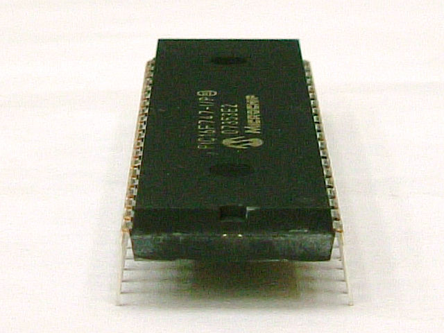
Why would a company need to hack its own embedded device? Consider a factory automation line using PIC16F747-based motor drives. The original source code was lost in a server migration, and the sole working unit is degrading. Without extraction, thousands of machines become obsolete. Our service lets you retrieve the firmware from that last good sample, then duplicate it onto fresh MCUs – saving millions in redesign costs. Similarly, medical syringe pumps with encrypted program logic can be decoded for safety recertification or feature enhancement. End users benefit from: (1) avoiding costly hardware re-engineering, (2) extending product life cycles, (3) creating backup archives for legacy repair, and (4) legally cloning batches of discontinued chips. Unlike reverse engineering for theft, our service requires proof of ownership. We turn a locked silicon puzzle into a usable heximal file – empowering you to maintain, upgrade, or migrate your embedded systems confidently.
Recover Chip ATmega261A Program
Recover Chip ATmega261A means the program of MCU ATmega261A from flash memory and eeprom memory will be readout and fuse bit of Microcontroller ATmega261A will be unlocked;
There are basically two types of interrupts. The first type is triggered by an event that sets the Interrupt Flag. For these interrupts, the Program Counter is vectored to the actual Interrupt Vector in order to execute the interrupt handling routine, and hardware clears the corresponding Interrupt Flag.
Interrupt Flags can also be cleared by writing a logic one to the flag bit position(s) to be cleared. If an interrupt condition occurs while the corresponding interrupt enable bit is cleared, the Interrupt Flag will be set and remembered until the interrupt is enabled, or the flag is cleared by software if break mcu atmega64pa binary.
Similarly, if one or more interrupt conditions occur while the Global Interrupt Enable bit is cleared, the corresponding Interrupt Flag(s) will be set and remembered until the Global Interrupt Enable bit is set, and will then be executed by order of priority.
The second type of interrupts will trigger as long as the interrupt condition is present. These interrupts do not necessarily have Interrupt Flags. If the interrupt condition disappears before the interrupt is enabled, the interrupt will not be triggered after break ic atmega128a firmware.
When the AVR exits from an interrupt, it will always return to the main program and execute one more instruction before any pending interrupt is served. Note that the Status Register is not automatChipally stored when entering an interrupt routine, nor restored when returning from an interrupt routine.
This must be handled by software. When using the CLI instruction to disable interrupts, the interrupts will be immediately disabled. No interrupt will be executed after the CLI instruction, even if it occurs simultaneously with the CLI instruction. The following example shows how this can be used to avoid interrupts during the timed EEPROM write sequence.
The interrupt execution response for all the enabled AVR interrupts is five clock cycles minimum. After five clock cycles the program vector address for the actual interrupt handling routine is executed. During these five clock cycle period, the Program Counter is pushed onto the Stack when Recover ic atmega168pa program.
The vector is normally a jump to the interrupt routine, and this jump takes three clock cycles. If an interrupt occurs during execution of a multi-cycle instruction, this instruction is completed before the interrupt is served.
If an interrupt occurs when the MCU is in sleep mode, the interrupt execution response time is increased by five clock cycles. This increase comes in addition to the start-up time from the selected sleep mode.
A return from an interrupt handling routine takes five clock cycles. During these five clock cycles, the Program Counter (three bytes) is popped back from the Stack, the Stack Pointer is incremented by three, and the I-bit in SREG is set.
 Posted in Recover Chip |
  Tags: recover chip embedded archive, recover chip embedded code, recover chip embedded content, recover chip embedded data, recover chip embedded eeprom, recover chip embedded file, recover chip embedded firmware, recover chip embedded information, recover chip embedded memory, recover chip embedded program |
  Comments Closed
Recover MCU ATtiny88A Program
Recover MCU ATtiny88A Program from secured flash memory, unlock microcontroller attiny88a security fuse bit by focus ion beam skill and read the firmware from microprocessor attiny88a memory;
The ATtiny48/88 is a low-power CMOS 8-bit microcontroller based on the AVR enhanced RISC architecture. By executing powerful instructions in a single clock cycle, the ATtiny48/88 achieves throughputs approaching 1 MIPS per MHz allowing the system designer to optimize power consumption versus processing speed.
The AVR core combines a rich instruction set with 32 general purpose working registers. All the 32 registers are directly connected to the Arithmetic Logic Unit (ALU), allowing two independent registers to be accessed in one single instruction executed in one clock cycle if Reverse engineering pic18f248 MCU.
The resulting architecture is more code efficient while achieving throughputs up to ten times faster than conventional CISC microcontrollers. The ATtiny48/88 provides the following features: 4/8K bytes of In-System Programmable Flash, 64/64 bytes EEPROM, 256/512 bytes SRAM, 24 general purpose I/O lines (28 I/Os in 32-lead TQFP and 32-pad QFN/MLF packages).
32 general purpose working registers, two flexible Timer/Counters with compare modes, internal and external interrupts, a byte-oriented 2-wire serial interface, an SPI serial port, a 6-channel 10-bit ADC (8 channels in 32-lead TQFP and 32-pad QFN/MLF packages), a programmable Watchdog Timer with internal oscillator, and three software selectable power saving modes.
Idle mode stops the CPU while allowing Timer/Counters, 2-wire serial interface, SPI port, and interrupt system to continue functioning. Power-down mode saves the register contents but freezes the oscillator, disabling all other MCU functions until the next interrupt or hardware reset. ADC Noise Reduction mode stops the CPU and all I/O modules except ADC, and helps to minimize switching noise during ADC conversions.
The device is manufactured using Atmel’s high density non-volatile memory technology. The On-MCU ISP Flash allows the program memory to be reprogrammed In-System through an SPI serial interface, by a conventional non-volatile memory programmer, or by an on-MCU boot program running on the AVR core.
The boot program can use any interface to download the application program in the Flash memory. By combining an 8-bit RISC CPU with In-System Self-Programmable Flash on a monolithic MCU, the Atmel ATtiny48/88 is a powerful microcontroller that provides a highly flexible and cost effective solution to many embedded control applications.
The ATtiny48/88 AVR is supported by a full suite of program and system development tools including: C compilers, macro assemblers, program debugger/simulators and evaluation kits. This documentation contains simple code examples that briefly show how to use various parts of the device.
These code examples assume that the part specific header file is included before compilation. Be aware that not all C compiler vendors include bit definitions in the header files and interrupt handling in C is compiler dependent. Please confirm with the C compiler documentation for more details.
For I/O Registers located in extended I/O map, “IN”, “OUT”, “SBIS”, “SBIC”, “CBI”, and “SBI” instructions must be replaced with instructions that allow access to extended I/O. Typically “LDS” and “STS” combined with “SBRS”, “SBRC”, “SBR”, and “CBR”.
Reliability Qualification results show that the projected data retention failure rate is much less than 1 PPM over 20 years at 85°C or 100 years at 25°C. Typical values contained in this datasheet are based on simulations and characterization of other AVR microcontrollers manufactured on the same process technology. Min and Max values will be available after the device is characterized.
Posted in Recover Chip |
Tags: recover mcu embedded archive, recover mcu embedded bin, recover mcu embedded code, recover mcu embedded content, recover mcu embedded data, recover mcu embedded eeprom, recover mcu embedded file, recover mcu embedded firmware, recover mcu embedded hex, recover mcu embedded information, recover mcu embedded memory, recover mcu embedded program |
Comments Closed
Recover MCU ATtiny88V Software
Recover MCU ATtiny88V Software and make the firmware cloning from master attiny88v which will provide the same functions, program from attiny88v memory will be readout by programmer;
The Stack is mainly used for storing temporary data, for storing local variables and for storing return addresses after interrupts and subroutine calls. The Stack Pointer Register always points to the top of the Stack. Note that the Stack is implemented as growing from higher memory locations to lower memory locations when Recover Mcu pic16f628 firmware.
This implies that a Stack PUSH command decreases the Stack Pointer. The Stack Pointer points to the data SRAM Stack area where the Subroutine and Interrupt Stacks are located. This Stack space in the data SRAM must be defined by the program before any subroutine calls are executed or interrupts are enabled.
The Stack Pointer must be set to point above 0x0200. The initial value of the stack pointer is the last address of the internal SRAM. The Stack Pointer is decremented by one when data is pushed onto the Stack with the PUSH instruction, and it is decremented by three when the return address is pushed onto the Stack with subroutine call or interrupt.
The Stack Pointer is incremented by one when data is popped from the Stack with the POP instruction, and it is incremented by three when data is popped from the Stack with return from subroutine RET or return from interrupt RETI after break pic12hv615 Mcu.
The AVR Stack Pointer is implemented as two 8-bit registers in the I/O space. The number of bits actually used is implementation dependent. Note that the data space in some implementations of the AVR architecture is so small that only SPL is needed.
In this case, the SPH Register will not be present. This section describes the general access timing concepts for instruction execution. The AVR CPU is driven by the CPU clock clkCPU, directly generated from the selected clock source for the chip. No internal clock division is used.
Figure 9 shows the parallel instruction fetches and instruction executions enabled by the Harvard architecture and the fast-access Register File concept. This is the basic pipelining concept to obtain up to 1 MIPS per MHz with the corresponding unique results for functions per cost, functions per clocks, and functions per power-unit.
The AVR provides several different interrupt sources. These interrupts and the separate Reset Vector each have a separate program vector in the program memory space. All interrupts are assigned individual enable bits which must be written logic one together with the Global Interrupt Enable bit in the Status Register in order to enable the interrupt.
Depending on the Program Counter value, interrupts may be automatically disabled when Boot Lock bits BLB02 or BLB12 are programmed. This feature improves software security.
The lowest addresses in the program memory space are by default defined as the Reset and Interrupt Vectors. The complete list of vectors is shown in “Interrupts” on page 69. The list also determines the priority levels of the different interrupts. The lower the address the higher is the priority level.
RESET has the highest priority, and next is INT0 – the External Interrupt Request 0. The Interrupt Vectors can be moved to the start of the Boot Flash section by setting the IVSEL bit in the MCU Control Register (MCUCR).
Refer to “Interrupts” on page 69 for more information. The Reset Vector can also be moved to the start of the Boot Flash section by programming the BOOTRST Fuse. When an interrupt occurs, the Global Interrupt Enable I-bit is cleared and all interrupts are disabled.
The user software can write logic one to the I-bit to enable nested inter rupts. All enabled interrupts can then interrupt the current interrupt routine. The I-bit is automatically set when a Return from Interrupt instruction – RETI – is executed.
Posted in Recover Chip |
Tags: recover mcu embedded archive, recover mcu embedded binary, recover mcu embedded code, recover mcu embedded content, recover mcu embedded data, recover mcu embedded eeprom, recover mcu embedded file, recover mcu embedded firmware, recover mcu embedded heximal, recover mcu embedded information, recover mcu embedded memory, recover mcu embedded program |
Comments Closed
Break IC ATtiny88 Heximal
Break IC ATtiny88 flash and eeprom memory, then readout Heximal from MCU ATtiny88 program memory, unlock microcontroller attiny88 security fuse bit and extract the embedded firmware;
High Performance, Low Power AVR® 8-Bit Microcontroller
Advanced RISC Architecture
– 123 Powerful Instructions – Most Single Clock Cycle Execution
– 32 x 8 General Purpose Working Registers
– Fully Static Operation if reverse engineering microcontroller pic16c558a
High Endurance Non-volatile Memory Segments
– 4K/8K Bytes of In-System Self-Programmable Flash program memory(ATtiny48/88)
– 64/64 Bytes EEPROM (ATtiny48/88)
– 256/512 Bytes Internal SRAM (ATtiny48/88)
– Write/Erase Cycles: 10,000 Flash/100,000 EEPROM
– Data retention: 20 years at 85°C / 100 years at 25°C
– Programming Lock for Software Security
Peripheral Features
– One 8-bit Timer/Counter with Separate Prescaler and Compare Mode
– One 16-bit Timer/Counter with Prescaler, and Compare and Capture Modes
– 8-channel 10-bit ADC in 32-lead TQFP and 32-pad QFN/MLF package
– 6-channel 10-bit ADC in 28-pin PDIP and 28-pad QFN/MLF package
– Master/Slave SPI Serial Interface
– Byte-oriented 2-wire Serial Interface (Philips I2C Compatible)
– Programmable Watchdog Timer with Separate On-chip Oscillator
– On-chip Analog Comparator
– Interrupt and Wake-up on Pin Change
Special Microcontroller Features
– debugWIRE On-chip Debug System
– In-System Programmable via SPI Port
– Power-on Reset and Programmable Brown-out Detection
– Internal Calibrated Oscillator before Break mcu pic12f519 binary
– External and Internal Interrupt Sources
– Three Sleep Modes: Idle, ADC Noise Reduction and Power-down I/O and Packages
– 28 Programmable I/O Lines in 32-lead TQFP and 32-pad QFN/MLF package
– 24 Programmable I/O Lines in 28-pin PDIP and 28-pad QFN/MLF package
– 28-pin PDIP, 32-lead TQFP, 28-pad QFN/MLF and 32-pad QFN/MLF
Operating Voltage:
– 1.8 – 5.5V
Temperature Range:
– -40°C to +85°C
Speed Grade:
– 0 – 4 MHz @ 1.8 – 5.5V
– 0 – 8 MHz @ 2.7 – 5.5V
– 0 – 12 MHz @ 4.5 – 5.5V
– Active Mode: 1 MHz, 1.8V: 240µA
– Power-down Mode: 0.1µA at 1.8V
Port A is a 4-bit bi-directional I/O port with internal pull-up resistors (selected for each bit) in 32-lead TQFP and 32-pad QFN/MLF package. The PA3..0 output buffers have symmetrical drive characteristics with both high sink and source capability.
As inputs, Port A pins that are externally pulled low will source current if the pull-up resistors are activated. The Port A pins are tristated when a reset condition becomes active, even if the clock is not running.
Posted in Break IC |
Tags: attack ATtiny88 mcu, break attiny88 mcu, crack ATtiny88 mcu, hack ATtiny88 mcu |
Comments Closed
Break IC ATtiny48A Software
Break IC ATtiny48A secured system and readout mcu attiny48a software from memory which include eeprom and flash, clone microcontroller attiny48a source code;
The Stack is mainly used for storing temporary data, for storing local variables and for storing return addresses after interrupts and subroutine calls. The Stack Pointer Register always points to the top of the Stack. Note that the Stack is implemented as growing from higher memory locations to lower memory locations when reverse engineering microcontroller pic16f73.
This implies that a Stack PUSH command decreases the Stack Pointer. The Stack Pointer points to the data SRAM Stack area where the Subroutine and Interrupt Stacks are located. This Stack space in the data SRAM must be defined by the program before any subroutine calls are executed or interrupts are enabled.
The Stack Pointer must be set to point above 0x0200. The initial value of the stack pointer is the last address of the internal SRAM. The Stack Pointer is decremented by one when data is pushed onto the Stack with the PUSH instruction, and it is decremented by three when the return address is pushed onto the Stack with subroutine call or interrupt before Break pic16c74 code.
The Stack Pointer is incremented by one when data is popped from the Stack with the POP instruction, and it is incremented by three when data is popped from the Stack with return from subroutine RET or return from interrupt RETI.
The AVR Stack Pointer is implemented as two 8-bit registers in the I/O space. The number of bits actually used is implementation dependent. Note that the data space in some implementations of the AVR architecture is so small that only SPL is needed.
In this case, the SPH Register will not be present. This section describes the general access timing concepts for instruction execution. The AVR CPU is driven by the CPU clock clkCPU, directly generated from the selected clock source for the chip. No internal clock division is used when recover chip pic16c77 flash.
Figure 9 shows the parallel instruction fetches and instruction executions enabled by the Harvard architecture and the fast-access Register File concept. This is the basic pipelining concept to obtain up to 1 MIPS per MHz with the corresponding unique results for functions per cost, functions per clocks, and functions per power-unit.
The AVR provides several different interrupt sources. These interrupts and the separate Reset Vector each have a separate program vector in the program memory space. All interrupts are assigned individual enable bits which must be written logic one together with the Global Interrupt Enable bit in the Status Register in order to enable the interrupt before Break IC.
Depending on the Program Counter value, interrupts may be automatically disabled when Boot Lock bits BLB02 or BLB12 are programmed. This feature improves software security. See the section “Memory Programming” on page 335 for details.
The lowest addresses in the program memory space are by default defined as the Reset and Interrupt Vectors. The complete list of vectors is shown in “Interrupts” on page 69. The list also determines the priority levels of the different interrupts. The lower the address the higher is the priority level.
RESET has the highest priority, and next is INT0 – the External Interrupt Request 0. The Interrupt Vectors can be moved to the start of the Boot Flash section by setting the IVSEL bit in the MCU Control Register (MCUCR).
Refer to “Interrupts” on page 69 for more information. The Reset Vector can also be moved to the start of the Boot Flash section by programming the BOOTRST Fuse, see “Memory Programming” on page 335.
When an interrupt occurs, the Global Interrupt Enable I-bit is cleared and all interrupts are disabled. The user software can write logic one to the I-bit to enable nested interrupts. All enabled interrupts can then interrupt the current interrupt routine. The I-bit is automatically set when a Return from Interrupt instruction – RETI – is executed.
Posted in Break IC |
Tags: attack attiny48a mcu, crack mcu attiny48a, hack attiny48a mcu |
Comments Closed
Copy Microcontroller PIC16F639 Heximal
Copy Microcontroller PIC16F639 Heximal needs to extract the flash program from microprocessor PIC16F639 and then crack microcontroller pic16f639 security fuse bit;
A single comparator is shown in Figure 6-1, along with the relationship between the analog input levels and the digital output. When the analog input at VIN+ is less than the analog input VIN-, the output of the comparator is a digital low level. When the analog input at VIN+ is greater than the analog input VIN-, the output of the comparator is a digital high level. The shaded areas of the output of the comparator in Figure 6-1 represent the uncertainty due to input offsets and response time.
The polarity of the comparator output can be inverted by setting the CINV bit (CMCON<4>). Clearing CINV results in a non-inverted output. A complete table showing the output state versus input conditions and VIN-the polarity bit.
There are eight modes of operation for the comparator. The CMCON register, shown in Register 6-1, is used to select the mode. Figure 6-2 shows the eight possible modes. The TRISA register controls the data direction of the comparator pins for each mode.
If the Comparator mode is changed, the comparator output
The CMCON register, shown in Register 6-1, is used to select the mode. Figure 6-2 shows the eight possible modes. The TRISA register controls the data direction of the comparator pins for each mode.
A simplified circuit for an analog input is shown in Figure 6-3. Since the analog pins are connected to a digital output, they have reverse biased diodes to VDD and VSS. The analog input, therefore, must be between VSS and VDD. If the input voltage deviates from this libri the polarity bit.
Response time is the minimum time, after selecting a new reference voltage or input source, before the comparator output is ensured to have a valid level. If the internal reference is changed, the maximum delay of the internal voltage reference must be considered when using the comparator outputs. Otherwise, the maximum delay of the comparators should be used H-CN;
Posted in Reverse Engineer Microcontroller |
Tags: copy microcontroller source bin, copy microcontroller source content, copy microcontroller source data, copy microcontroller source file, copy microcontroller source flash, copy microcontroller source hex, copy microcontroller source software |
Comments Closed
Break IC ATmega128A Eprom
Break IC ATmega128A Eprom memory and restore the embedded firmware from atmega128a flash memory, the firmware of atmega128a microcontroller can be readout directly after reset the status.
The Atmel QTouch Library provides a simple to use solution to realize touch sensitive interfaces on most Atmel AVR microcontrollers. The QTouch Library includes support for the QTouch and QMatrix acquisition methods.
Touch sensing can be added to any application by linking the appropriate Atmel QTouch Library for the AVR Microcontroller. This is done by using a simple set of APIs to define the touch channels and sensors, and then calling the touch sensing API’s to retrieve the channel information and determine the touch sensor states if reverse engineering microcontroller attiny461.
The QTouch Library is FREE and downloadable from the Atmel website at the following location: www.atmel.com/qtouchlibrary. For implementation details and other information, refer to the Atmel QTouch Library User Guide – also available for download from the Atmel website.
First Analog Comparator conversion may be delayed Interrupts may be lost when writing the timer registers in the asynchronous timer Stabilizing time needed when changing XDIV Register
Stabilizing time needed when changing OSCCAL Register
IDCODE masks data from TDI input
Breaking EEPROM by using ST or STS to set EERE bit triggers unexpected interrupt request
First Analog Comparator conversion may be delayed
If the device is powered by a slow rising VCC, the first Analog Comparator conversion will take longer than expected on some devices if reverse engineering microcontroller atmega640.
Problem Fix/Workaround
When the device has been powered or reset, disable then enable theAnalog Comparator before the first conversion.
Interrupts may be lost when writing the timer registers in the asynchronous timer
The interrupt will be lost if a timer register that is synchronous timer clock is written when the asynchronous Timer/Counter register (TCNTx) is 0x00.
Problem Fix/Workaround
Always check that the asynchronous Timer/Counter register neither have the value 0xFF nor 0x00 before writing to the asynchronous Timer Control Register (TCCRx), asynchronous Timer Counter Register (TCNTx), or asynchronous Output Compare Register (OCRx).
Stabilizing time needed when changing XDIV Register
After increasing the source clock frequency more than 2% with settings in the XDIV register, the device may execute some of the subsequent instructions incorrectly when Break IC.
Problem Fix / Workaround
The NOP instruction will always be executed correctly also right after a frequency change.
Thus, the next 8 instructions after the change should be NOP instructions. To ensure this, follow this procedure:
1.Clear the I bit in the SREG Register.
2.Set the new pre-scaling factor in XDIV register.
3.Execute 8 NOP instructions
4.Set the I bit in SREG
This will ensure that all subsequent instructions will execute correctly.
Assembly Code Example:
Stabilizing time needed when changing OSCCAL Register before Break IC
After increasing the source clock frequency more than 2% with settings in the OSCCAL register, the device may execute some of the subsequent instructions incorrectly.
Problem Fix / Workaround
The behavior follows errata number 3., and the same Fix / Workaround is applicable on this errata.
IDCODE masks data from TDI input
The JTAG instruction IDCODE is not working correctly. Data to succeeding devices are replaced by all-ones during Update-DR.
Problem Fix / Workaround
If ATmega128 is the only device in the scan chain, the problem is not visible.
Select the Device ID Register of the ATmega128 by issuing the IDCODE instruction or by entering the Test-Logic-Reset state of the TAP controller to break out the contents of its Device ID Register and possibly data from succeeding devices of the scan chain. Issue the BYPASS instruction to the ATmega128 while breaking the Device ID Registers of preceding devices of the boundary scan chain.
If the Device IDs of all devices in the boundary scan chain must be captured simultaneously, the ATmega128 must be the fist device in the chain.
Breaking EEPROM by using ST or STS to set EERE bit triggers unexpected interrupt request.
Breaking EEPROM by using the ST or STS command to set the EERE bit in the EECR register triggers an unexpected EEPROM interrupt request.
Problem Fix / Workaround
Always use OUT or SBI to set EERE in EECR.
Reverse Engineering Microcontroller ATmega16PA Heximal
Reverse Engineering Microcontroller ATmega16PA to locate the security fuse bit of mcu atmega16pa, crack mcu atmega16pa fuse bit and readout embedded Heximal from mcu atmega16pa eeprom and flash memory;
First Analog Comparator conversion may be delayed, If the device is powered by a slow rising VCC, the first Analog Comparator conversion will take longer than expected on some devices.
Problem Fix/Workaround
When the device has been powered or reset, disable then enable the Analog Comparator before the first conversion.
Interrupts may be lost when writing the timer registers in the asynchronous timer, The interrupt will be lost if a timer register that is synchronized to the asynchronous timer clock is written when the asynchronous Timer/Counter register (TCNTx) is 0x00.
Problem Fix / Workaround
Always check that the asynchronous Timer/Counter register neither have the value 0xFF nor 0x00 before writing to the asynchronous Timer Control Register (TCCRx), asynchronous Timer Counter Register(TCNTx), or asynchronous Output Compare Register (OCRx).
IDCODE masks data from TDI input
The JTAG instruction IDCODE is not working correctly. Data to succeeding devices are replaced by all-ones during Update-DR.
Problem Fix / Workaround
If ATmega16 is the only device in the scan chain, the problem is not visible. Select the Device ID Register of the ATmega16 by issuing the IDCODE instruction or by entering the Test-Logic-Reset state of the TAP controller to reverse engineering out the contents of its Device ID Register and possibly data from succeeding devices of the scan chain. Issue the BYPASS instruction to the ATmega16.
Registers of preceding devices of the boundary scan chain.
If the Device IDs of all devices in the boundary scan chain must be captured simultaneously, the ATmega16 must be the fist device in the chain.
Reverse engineeringing EEPROM by using ST or STS to set EERE bit triggers unexpected interrupt request.
Reverse engineeringing EEPROM by using the ST or STS command to set the EERE bit in the EECR register triggers an unexpected EEPROM interrupt request.
Problem Fix / Workaround
Always use OUT or SBI to set EERE in EECR.
First Analog Comparator conversion may be delayed
If the device is powered by a slow rising VCC, the first Analog Comparator conversion will take longer than expected on some devices.
Problem Fix/Workaround
When the device has been powered or reset, disable then enable the Analog Comparator before the first conversion.
Interrupts may be lost when writing the timer registers in the asynchronous timer
The interrupt will be lost if a timer register that is synchronized to the asynchronous timer clock is written when the asynchronous Timer/Counter register(TCNTx) is 0x00.
Problem Fix / Workaround
Always check that the asynchronous Timer/Counter register neither have the value 0xFF nor 0x00 before writing to the asynchronous Timer Control Register(TCCRx), asynchronous Timer Counter Register(TCNTx), or asynchronous Output Compare Register(OCRx).
IDCODE masks data from TDI input
The JTAG instruction IDCODE is not working correctly. Data to succeeding devices are replaced by all-ones during Update-DR.
Problem Fix / Workaround
If ATmega16 is the only device in the scan chain, the problem is not visible.
Select the Device ID Register of the ATmega16 by issuing the IDCODE instruction or by entering the Test-Logic-Reset state of the TAP controller to reverse engineering out the contents of its Device ID Register and possibly data from succeeding devices of the scan chain. Issue the BYPASS instruction to the ATmega16 while reverse engineeringing the Device ID
Registers of preceding devices of the boundary scan chain. If the Device IDs of all devices in the boundary scan chain must be captured.
Posted in Recover Chip |
Tags: reverse engineering microcontroller embedded archive, reverse engineering microcontroller embedded bin, reverse engineering microcontroller embedded code, reverse engineering microcontroller embedded content, reverse engineering microcontroller embedded data, reverse engineering microcontroller embedded eeprom, reverse engineering microcontroller embedded file, reverse engineering microcontroller embedded firmware, reverse engineering microcontroller embedded hex, reverse engineering microcontroller embedded information, reverse engineering microcontroller embedded memory, reverse engineering microcontroller embedded program |
Comments Closed