Archive for the ‘Break IC’ Category
 Secured Microcontroller Hardware Security
 April 10th, 2019 |
  Author:
 When the existence of a backdoor in highly secure Microcontrollers was discovered in the form of secret test/debug interface capable of overriding chip security policy, it raised a lot of questions about Secured Microcontroller Hardware Security of modern ICs.
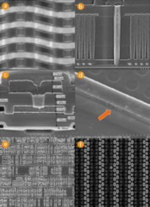
Secured Microcontroller Hardware Security
Recently demonstrated method for the direct imaging of EEPROM and Flash memory contents using easily accessible Scanning Electron Microscopes (SEM) challenges the security of embedded storage. This is because non-volatile memory was always considered as being highly secure against most invasive MCU crack due to very small electrical charge accumulated beneath very thin barrier that cannot survive de-processing. Now the obvious question is: What could be the next in ground IC breaking and disturbing attack on hardware security?
In many cases new MCU attacks were far from being something absolutely new. For example, structural analysis for impurities using chemical methods were known for decades and actively used in Failure Analysis. The fact that switching of each individual transistor contributes to the overall power consumption of the circuit was not new and was actively used by semiconductors development tools to predict power consumption and overheating. Even the photon emission was known, but was too expensive as common attack technology.
The fact that photons can interact with transistors was known since the development of transistors and was even used for communication. The ability of electron beam to detect buried charge was also known, but only with the development of more sensitive microscopes became practical to use. The main message of this paper is if the vast majority of IC code extraction are based on already known facts, there must be a way to predict such attacks and develop mitigation techniques well ahead of the active use by attackers.
 Posted in
PIC18F4523 Microcontroller Embedded Memory Breaking
Many PIC18 control instructions do not need any argument at all by Break IC STM32F101C4T6TR Binary; they either perform an operation that globally affects the device or they operate implicitly on one register after PIC18F4523 Microcontroller Embedded Memory Breaking. This addressing mode is known as Inherent Addressing. Examples include SLEEP, RESET and DAW.
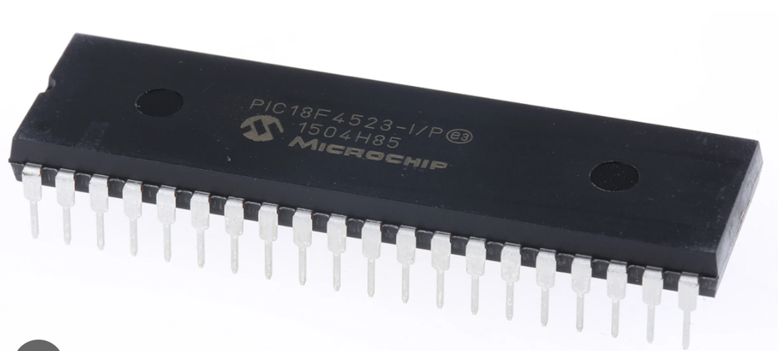
quebrar o bit de fusível do microcontrolador protegido MICROCHIP PIC18F4523 para restaurar o código-fonte protetor MCU PIC18F4523 da memória flash do programa e da memória eeprom de dados, copiar o código-fonte no formato de arquivo binário ou software heximal para o novo microprocessador MICROCHIP PIC18F4523;
Other instructions work in a similar way but require an additional explicit argument in the opcode to Break Chip SAF-C164CI-8EM Firmware. This is known as Literal Addressing mode because they require some literal value as an argument. Examples include ADDLW and MOVLW, which respectively, add or move a literal value to the W register. Other examples include CALL and GOTO, which include a 20-bit program memory address.
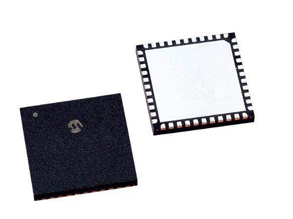
cracker le bit de fusible du microcontrôleur sécurisé MICROCHIP PIC18F4523 pour restaurer le code source de protection du MCU PIC18F4523 à partir de la mémoire flash du programme et de la mémoire eeprom de données, copier le code source au format de fichier binaire ou de logiciel heximal vers le nouveau microprocesseur MICROCHIP PIC18F4523 ;
Direct Addressing mode specifies all or part of the source and/or destination address of the operation within the opcode itself. The options are specified by the arguments accompanying the instruction.
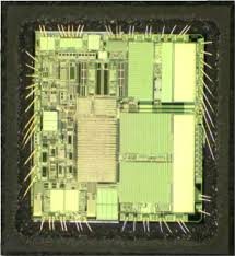
PIC18F4523 Microcontroller Embedded Memory Breaking
In the core PIC18 instruction set, bit-oriented and byte- oriented instructions use some version of Direct Addressing by default to better support Break Microcontroller PIC12F629 Program. All of these instructions include some 8-bit literal address as their Least Significant Byte when PIC18F4523 Microcontroller Embedded Memory Breaking. This address specifies either a register address in one of the banks of data RAM through Crack MCU memory.
The Access RAM bit ‘a’ determines how the address is interpreted. When ‘a’ is ‘1’, the contents of the BSR (Section 5.3.1 “Bank Select Register (BSR)”) are used with the address to determine the complete 12-bit address of the register. When ‘a’ is ‘0’, the address is interpreted as being a register in the Access Bank to facilitate the process of Break MCU dsPIC30F4011 Heximal. Addressing that uses the Access RAM is sometimes also known as Direct Forced Addressing mode.
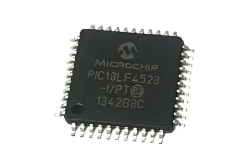
złamanie zabezpieczonego bezpiecznika mikrokontrolera MICROCHIP PIC18F4523 w celu przywrócenia ochronnego kodu źródłowego MCU PIC18F4523 z pamięci flash programu i pamięci eeprom danych, skopiowanie kodu źródłowego w formacie pliku binarnego lub oprogramowania szesnastkowego do nowego mikroprocesora MICROCHIP PIC18F4523;
Microprocessor PIC18F4510 Eeprom Memory Breaking
Protective microprocessor PIC18F4510 eeprom data memory and flash program memory breaking needs to crack secured MICROCHIP MCU PIC18F4510 fuse bit, unlock microcontroller PIC18F4510 and readout embedded firmware in the format of binary file or heximal data;
While the use of the BSR with an embedded 8-bit address allows users to address the entire range of data memory which can facilitate Microprocessor PIC18F4510 Eeprom Memory Breaking, it also means that the user must always ensure that the correct bank is selected. Otherwise, data may be read from or written to the wrong location.
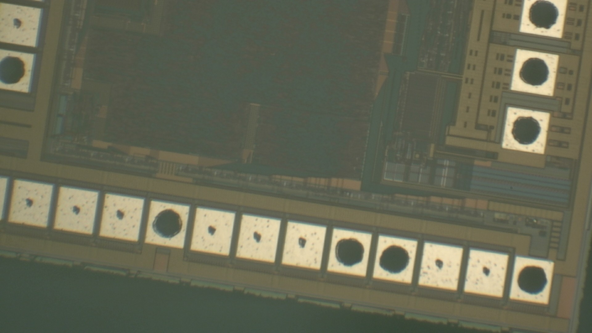
la memoria dati eeprom del microprocessore protettivo PIC18F4510 e la rottura della memoria del programma flash necessitano di crack protetti, bit fusibile MICROCHIP MCU PIC18F4510, sblocco del microcontrollore PIC18F4510 e lettura del firmware incorporato nel formato di file binario o dati essimali;
This can be disastrous if a GPR is the intended target of an operation, but an SFR is written to instead. Verifying and/or changing the BSR for each read or write to data memory can become very inefficient.
To streamline access for the most commonly used data memory locations, the data memory is configured with an Access Bank, which allows users to access a mapped block of memory without specifying a BSR. The Access Bank consists of the first 128 bytes of memory (00h-7Fh) in Bank 0 and the last 128 bytes of memory (80h-FFh) in Block 15.
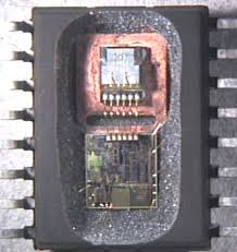
Microprocessor PIC18F4510 Eeprom Memory Breaking
The lower half is known as the “Access RAM” and is composed of GPRs. This upper half is also where the device’s SFRs are mapped. These two areas are mapped contiguously in the Access Bank and can be addressed in a linear fashion by an 8-bit address.

koruyucu mikroişlemci PIC18F4510 eeprom veri belleği ve flash program belleği kırma, güvenli MICROCHIP MCU PIC18F4510 sigorta bitini kırmalı, mikrodenetleyici PIC18F4510’un kilidini açmalı ve yerleşik bellenimi ikili dosya veya onaltılı veri formatında okumalıdır;
The Access Bank is used by core PIC18F4510 instructions that include the Access RAM bit (the ‘a’ parameter in the instruction). When ‘a’ is equal to ‘1’, the instruction uses the BSR and the 8-bit address included in the opcode for the data memory address. When ‘a’ is ‘0’,
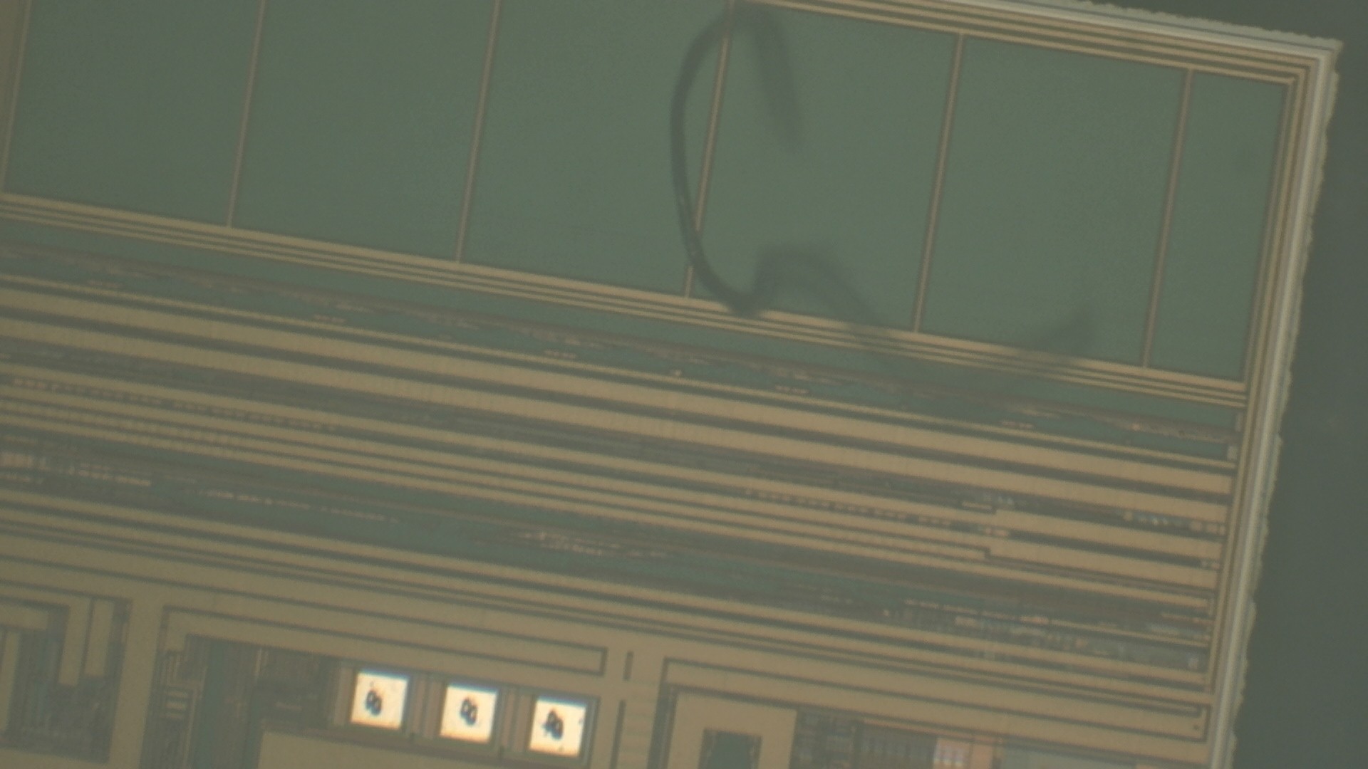
védő mikroprocesszor PIC18F4510 eeprom adatmemória és flash program memória feltörése fel kell törni a biztonságos MICROCHIP MCU PIC18F4510 biztosítékbitet, fel kell oldani a PIC18F4510 mikrovezérlőt és ki kell olvasni a beágyazott firmware-t bináris fájl vagy heximális adat formátumban;
Break Microchip PIC18F4439 Microprocessor Memory
Break Microchip PIC18F4439 microprocessor memory protection and recover embedded firmware from secured microcontroller PIC18F4439 flash program memory and eeprom data memory, copy binary source code or heximal software to new locked MCU PIC18F4439 as replication;
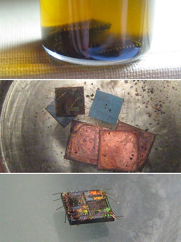
întrerupeți protecția memoriei microprocesorului Microcip PIC18F4439 și recuperați firmware-ul încorporat din memoria programului flash securizat de microcontroler PIC18F4439 și memoria de date eeprom, copiați codul sursă binar sau software-ul heximal în noul MCU blocat PIC18F4439 ca replicare;
There are three types of memory in PIC18F4439 Enhanced microcontroller devices which can be used for the purpose of Break Microchip PIC18F4439 Microprocessor Memory:
• Program Memory
• Data RAM
• Data EEPROM
As Harvard architecture devices, the data and program memories use separate busses; this allows for concurrent access of the two memory spaces. The data EEPROM, for practical purposes, can be regarded as a peripheral device, since it is addressed and accessed through a set of control registers when Copy MCU PIC32MX440F512H binary.
Additional detailed information on the operation of the Flash program memory is provided in Section 6.0 “Flash Program Memory”. Data EEPROM is discussed separately in Section 7.0 “Data EEPROM Memory”.

prolomit ochranu mikroprocesorové paměti Microchip PIC18F4439 a obnovit vestavěný firmware ze zabezpečené paměti flash programu PIC18F4439 a datové paměti eeprom, zkopírovat binární zdrojový kód nebo heximální software do nového uzamčeného MCU PIC18F4439 jako replikaci;
PIC18 microcontrollers implement a 21-bit program counter, which is capable of addressing a 2-Mbyte program memory space. Accessing a location between the upper boundary of the physically implemented memory and the 2-Mbyte address will return all ‘0’s (a NOP instruction) after Crack MCU Firmware.
The PIC18F4439 each have 16 Kbytes of Flash memory and can store up to 8,192 single-word instructions. The PIC18F4439 each have 32 Kbytes of Flash memory and can store up to 16,384 single-word instructions by Break Microchip PIC18F4439 Microprocessor Memory.
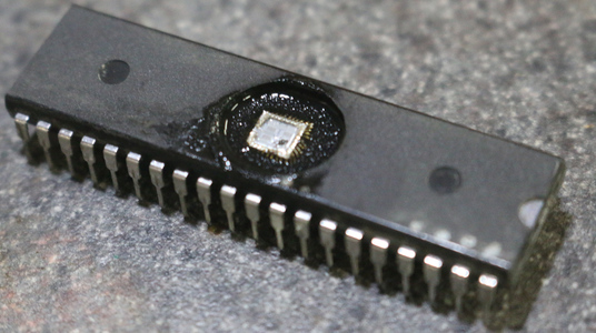
Break Microchip PIC18F4439 microprocessor memory protection and recover embedded firmware from secured microcontroller PIC18F4439 flash program memory and eeprom data memory, copy binary source code or heximal software to new locked MCU PIC18F4439 as replication;
PIC18 devices have two interrupt vectors. The Reset vector address is at 0000h and the interrupt vector addresses are at 0008h and 0018h. The program memory map for PIC18F4439 devices is shown in below Figure.
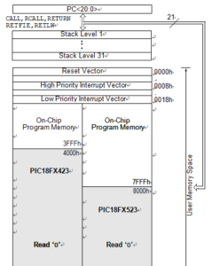
The Program Counter (PC) specifies the address of the instruction to fetch for execution. The PC is 21 bits wide and is contained in three separate 8-bit registers in order to Recover IC STM32F107RCT6 Code. The low byte, known as the PCL register, is both readable and writable.
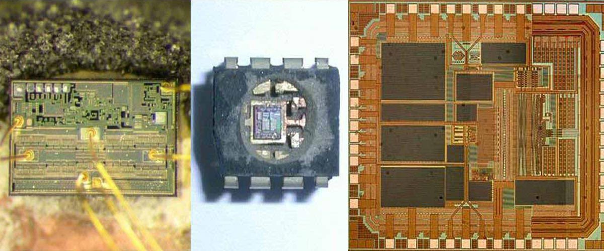
prekinuti zaštitu memorije Microchip PIC18F4439 mikroprocesora i oporaviti ugrađeni firmware iz osigurane flash programske memorije mikrokontrolera PIC18F4439 i eeprom podatkovne memorije, kopirati binarni izvorni kod ili heksimalni softver na novi zaključani MCU PIC18F4439 kao replikaciju;
The high byte, or PCH register, contains the PC<15:8> bits; it is not directly readable or writable. Updates to the PCH register are performed through the PCLATH register. The upper byte is called PCU. This register contains the PC<20:16> bits; it is also not directly readable or writable when Copy IC Atmega8L hex.
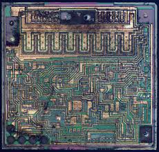
Break Microchip PIC18F4439 Microprocessor Memory
Updates to the PCU register are performed through the PCLATU register. The contents of PCLATH and PCLATU are transferred to the program counter by any operation that writes PCL to facilitate the process of Attack Chip DSPIC33FJ256GP506A Software. Similarly, the upper two bytes of the program counter are transferred to PCLATH and PCLATU by an operation that reads PCL. This is useful for computed offsets to the PC (see Section 5.1.4.1 “Computed GOTO”).
Break Microchip PIC18F4420 Microcontroller Memory
Break Microchip PIC18F4420 microcontroller memory including flash memory can help us extract protective PIC18F4420 microchip MCU embedded firmware content from its flash after disable the security fuse, restore binary file or heximal data of source code after decapsulate locked PIC18F4420 microprocessor;
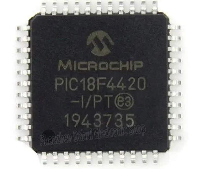
Break Microchip PIC18F4420 microcontroller memory including flash memory can help us extract protective PIC18F4420 microchip MCU embedded firmware content from its flash after disable the security fuse, restore binary file or heximal data of source code after decapsulate locked PIC18F4420 microprocessor
PIC18F4420 devices incorporate three separate on-chip timers that help regulate the Power-on Reset process when Crack MCU eprom. Their main function is to ensure that the device clock is stable before code is executed which can be manipulated in the process of Break Microchip PIC18F4420 Microcontroller Memory. These timers are:
• Power-up Timer (PWRT)
• Oscillator Start-up Timer (OST)
• PLL Lock Time-out
The Power-up Timer (PWRT) of PIC18F4420 devices is an 11-bit counter which uses the INTRC source as the clock input. This yields an approximate time interval of 2048 x 32 s= 65.6 ms. While the PWRT is counting, the device is held in Reset to Recover IC ST62T65C6 Software.
The power-up time delay depends on the INTRC clock and will vary from chip-to-chip due to temperature and process variation. See DC parameter 33 for details.
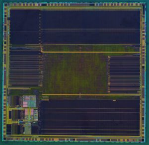
Break Microchip PIC18F4420 Microcontroller Memory
The PWRT is enabled by clearing the PWRTEN Configuration bit.
The Oscillator Start-up Timer (OST) provides a 1024 oscillator cycle (from OSC1 input) delay after the PWRT delay is over (parameter 33). This ensures that the crystal or resonator oscillator has started and is stable enough to clock the controller by Read MCU PIC16F688 Software. More time may be required for the oscillator to meet its frequency tolerance specification.
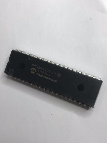
quebrar a memória do microcontrolador Microchip PIC18F4420, incluindo memória flash, pode nos ajudar a extrair o conteúdo do firmware incorporado do microchip MCU protetor PIC18F4420 de seu flash após desativar o fusível de segurança, restaurar arquivo binário ou dados heximais do código-fonte após desencapsular o microprocessador PIC18F4420 bloqueado;
The OST time-out is invoked only for XT, LP, HS and HSPLL modes and only on Power-on Reset, or on exit from most power-managed modes.
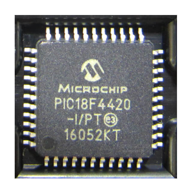
przerwanie pamięci mikrokontrolera Microchip PIC18F4420, w tym pamięci flash, może pomóc nam wyodrębnić ochronną zawartość wbudowanego oprogramowania układowego MCU mikrochip PIC18F4420 z jego pamięci flash po wyłączeniu bezpiecznika zabezpieczającego, przywróceniu pliku binarnego lub danych szesnastkowych kodu źródłowego po dekapsulacji zablokowanego mikroprocesora PIC18F4420;
With the PLL enabled in its PLL mode, the time-out sequence following a Power-on Reset is slightly differ- ent from other oscillator modes. A separate timer is used to provide a fixed time-out that is sufficient for the PLL to lock to the main oscillator frequency to support the process of Read IC Microchip PIC32MX440F512H Binary. This PLL lock time-out (TPLL) is typically 2 ms and follows the oscillator start-up time-out.
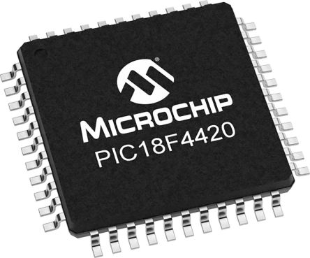
casser la mémoire du microcontrôleur Microchip PIC18F4420, y compris la mémoire flash, peut nous aider à extraire le contenu du micrologiciel intégré de protection de la puce PIC18F4420 MCU de son flash après avoir désactivé le fusible de sécurité, restaurer le fichier binaire ou les données heximales du code source après avoir décapsulé le microprocesseur PIC18F4420 verrouillé ;
Break PIC18F4331 Microprocessor Eeprom Memory
Break PIC18F4331 microprocessor eeprom memory can help engineer to restore embedded firmware from secured MCU PIC18F4331’s flash program memory and eeprom data memory, copy extracted source code to new microcontroller PIC18F4331 for cloning;
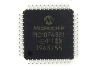
break PIC18F4331 microprocessor eeprom memory can help engineer to restore embedded firmware from secured MCU PIC18F4331’s flash program memory and eeprom data memory, copy extracted source code to new microcontroller PIC18F4331 for cloning
The MCLR pin provides a method for triggering an external Reset of the device by Break PIC18F4331 Microprocessor Eeprom Memory. A Reset is generated by holding the pin low. These devices have a noise filter in the MCLR Reset path which detects and ignores small pulses when Crack MCU Firmware.
The MCLR pin is not driven low by any internal Resets, including the WDT.
In PIC18F4331 devices, the MCLR input can be disabled with the MCLRE Configuration bit. When MCLR is disabled, the pin becomes a digital input. See Section 10.5 “PORTE, TRISE and LATE Registers” for more information.
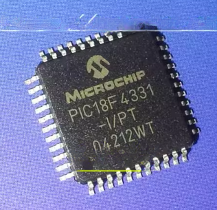
romper la memoria eeprom del microprocesador PIC18F4331 puede ayudar al ingeniero a restaurar el firmware integrado desde la memoria flash del programa MCU PIC18F4331 segura y la memoria de datos eeprom, copiar el código fuente extraído al nuevo microcontrolador PIC18F4331 para clonación
A Power-on Reset pulse is generated on-chip whenever VDD rises above a certain threshold after Break PIC18F2510 Microcontroller Flash Memory. This allows the device to start in the initialized state when VDD is adequate for operation.
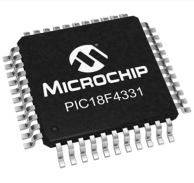
phá vỡ bộ nhớ eeprom của bộ vi xử lý PIC18F4331 có thể giúp kỹ sư khôi phục phần sụn nhúng từ bộ nhớ chương trình flash và bộ nhớ dữ liệu eeprom của MCU PIC18F4331 được bảo mật, sao chép mã nguồn đã trích xuất sang bộ vi điều khiển mới PIC18F4331 để nhân bản
To take advantage of the POR circuitry, tie the MCLR pin through a resistor (1 kÙ to 10 kÙ) to VDD. This will eliminate external RC components usually needed to create a Power-on Reset delay for the purpose of Copy PIC18F2480 MCU Locked Heximal. A minimum rise rate for VDD is specified (parameter D004). For a slow rise time, see below Figure.
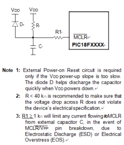
When the device starts normal operation (i.e., exits the Reset condition), device operating parameters (voltage, frequency, temperature, etc.) must be met to ensure operation. If these conditions are not met, the device must be held in Reset until the operating conditions are met for the purpose of Losted PIC18F2458 Microcontroller Embedded Code Restoration.
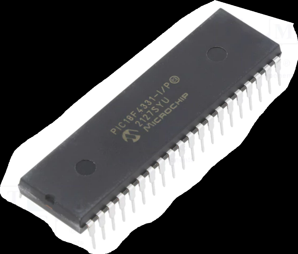
PIC18F4331 माइक्रोप्रोसेसर eeprom मेमोरी को तोड़ने से इंजीनियर को सुरक्षित MCU PIC18F4331 की फ्लैश प्रोग्राम मेमोरी और eeprom डेटा मेमोरी से एम्बेडेड फर्मवेयर को पुनर्स्थापित करने में मदद मिल सकती है, क्लोनिंग के लिए नए माइक्रोकंट्रोलर PIC18F4331 में निकाले गए स्रोत कोड की प्रतिलिपि बनाई जा सकती है
POR events are captured by the POR bit (RCON<1>). The state of the bit is set to ‘0’ whenever a POR occurs; it does not change for any other Reset event. POR is not reset to ‘1’ by any hardware event. To capture multiple events, the user manually resets the bit to ‘1’ in software following any POR by Microcontroller PIC18F2439 Code Reverse Engineering.
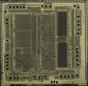
Break PIC18F4331 Microprocessor Eeprom Memory
Microchip PIC18F4321 Processor Flash Breaking
Microchip PIC18F4321 microprocessor flash memory breaking starts from decrypt secured MCU Microchip PIC18F4321 fuse bit and then extract binary source code or heximal data file from PIC18F4321 locked microcontroller flash program and eeprom memory;
Het breken van het flashgeheugen van de Microchip PIC18F4321 microprocessor begint met het decoderen van de beveiligde MCU Microchip PIC18F4321 fuse bit en het extraheren van de binaire broncode of het heximale gegevensbestand uit het PIC18F4321 vergrendelde flashprogramma van de microcontroller en het eeprom-geheugen;
Normally, the device is held in Reset by the Oscillator Start-up Timer (OST) by Microchip PIC18F4321 Processor Flash Breaking until the primary clock becomes ready. At that time, the OSTS bit is set and the device begins executing code. If the internal oscillator block is the new clock source, the IOFS bit is set instead when Unlock Microcontroller Flash.
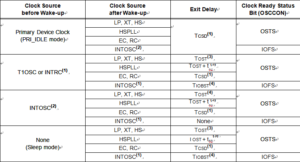
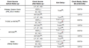
The exit delay time from Reset to the start of code execution depends on both the clock sources before and after the wake-up and the type of oscillator if the new clock source is the primary clock by Open IC PIC16F73 Memory,. Exit delays are summarized in below Table.
Code execution can begin before the primary clock becomes ready. If either the Two-Speed Start-up (see Section 23.3 “Two-Speed Start-up”) or Fail-Safe Clock Monitor (see Section 23.4 “Fail-Safe Clock Monitor”) is enabled, the device may begin execution as soon as the Reset source has cleared when Break Secured MCU PIC16F72 Data.
Microchip PIC18F4321 Processor Flash Breaking
Execution is clocked by the INTOSC multiplexer driven by the inter- nal oscillator block. Execution is clocked by the internal oscillator block until either the primary clock becomes ready or a power-managed mode is entered before the primary clock becomes ready; the primary clock is then shut down by Recover IC PIC16LF506 Data.
Microchip PIC18F4321 microprocessor flash memory breaking starts from decrypt secured MCU Microchip PIC18F4321 fuse bit and then extract binary source code or heximal data file from PIC18F4321 locked microcontroller flash program and eeprom memory;
Certain exits from power-managed modes do not invoke the OST at all. There are two cases:
• PRI_IDLE mode, where the primary clock source is not stopped and
• the primary clock source is not any of the LP, XT, HS or HSPLL modes.
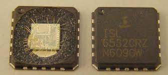
माइक्रोचिप PIC18F4321 माइक्रोप्रोसेसर फ्लैश मेमोरी ब्रेकिंग डिक्रिप्ट सुरक्षित MCU माइक्रोचिप PIC18F4321 फ्यूज बिट से शुरू होती है और फिर PIC18F4321 लॉक किए गए माइक्रोकंट्रोलर फ्लैश प्रोग्राम और ईप्रोम मेमोरी से बाइनरी सोर्स कोड या हेक्सिमल डेटा फ़ाइल निकालती है;
In these instances, the primary clock source is either already running (PRI_IDLE), or normally does not require an oscillator start-up delay (RC, EC and INTIO Oscillator modes). However, a fixed delay of interval TCSD following the wake event is still required when leaving Sleep and Idle modes to allow the CPU to prepare for execution when Decrypt Locked IC PIC16LF505 Program. Instruction execution resumes on the first clock cycle following this delay.
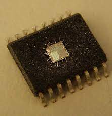
يبدأ كسر ذاكرة فلاش المعالج الدقيق PIC18F4321 من فك تشفير MCU المؤمن، Microchip PIC18F4321 بت الصمامات ثم استخراج كود المصدر الثنائي أو ملف البيانات السداسي من برنامج فلاش المتحكم الدقيق PIC18F4321 وذاكرة eeprom؛
Break PIC18F4220 Microcontroller Flash Memory
Break PIC18F4220 microcontroller flash memory and eeprom memory fuse bit to restore embedded firmware of binary program or heximal data from secured PIC18F4220 microprocessor, original protective MICROCHIP MCU PIC18F4220 decryption is a destructive process;
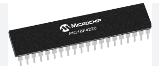
Break PIC18F4220 microcontroller flash memory and eeprom memory fuse bit to restore embedded firmware of binary program or heximal data from secured PIC18F4220 microprocessor, original protective MICROCHIP MCU PIC18F4220 decryption is a destructive process;
Normally, the device is held in Reset by the Oscillator Start-up Timer (OST) until the primary clock becomes ready from Break PIC18F4220 Microcontroller Flash Memory. At that time, the OSTS bit is set and the device begins executing code. If the internal oscillator block is the new clock source, the IOFS bit is set instead to Reverse Engineering ATMEL chip AT32UC3C264C flash.
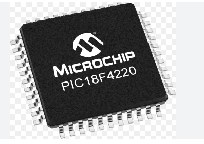
briser le bit de fusible de la mémoire flash du microcontrôleur PIC18F4220 et de la mémoire EEPROM pour restaurer le micrologiciel intégré du programme binaire ou des données hexadécimales du microprocesseur PIC18F4220 sécurisé, le décryptage du microprocesseur MICROCHIP MCU PIC18F4220 de protection d’origine est un processus destructeur ;
The exit delay time from Reset to the start of code execution depends on both the clock sources before and after the wake-up and the type of oscillator if the new clock source is the primary clock from Reverse Engineering Chip ATMEGA644A code, Exit delays are summarized in below Table.
Code execution can begin before the primary clock becomes ready. If either the Two-Speed Start-up (see Section 23.3 “Two-Speed Start-up”) or Fail-Safe Clock Monitor (see Section 23.4 “Fail-Safe Clock Monitor”) is enabled, the device may begin execution as soon as the Reset source has cleared after Unlock Microcontroller Eeprom.
breek het flashgeheugen en eeprom-geheugen van de PIC18F4220-microcontroller om de ingebouwde firmware van een binair programma of heximale gegevens van een beveiligde PIC18F4220-microprocessor te herstellen, originele beschermende MICROCHIP MCU PIC18F4220-decodering is een destructief proces;
Execution is clocked by the INTOSC multiplexer driven by the inter- nal oscillator block. Execution is clocked by the internal oscillator block until either the primary clock becomes ready or a power-managed mode is entered before the primary clock becomes ready before Reverse Engineering Microcontroller ATmega644PA firmware; the primary clock is then shut down.
Break PIC18F4220 Microcontroller Flash Memory
Certain exits from power-managed modes do not invoke the OST at all. There are two cases:
• PRI_IDLE mode, where the primary clock source is not stopped and
• the primary clock source is not any of the LP, XT, HS or HSPLL modes.
In these instances, the primary clock source is either already running (PRI_IDLE), or normally does not require an oscillator start-up delay (RC, EC and INTIO Oscillator modes) by Recover MCU ATmega162A Heximal. However, a fixed delay of interval TCSD following the wake event is still required when leaving Sleep and Idle modes to Break PIC18F4220 Microcontroller Flash Memory. Instruction execution resumes on the first clock cycle following this delay.
सुरक्षित PIC18F4220 माइक्रोप्रोसेसर से बाइनरी प्रोग्राम या हेक्सिमल डेटा के एम्बेडेड फर्मवेयर को पुनर्स्थापित करने के लिए PIC18F4220 माइक्रोकंट्रोलर फ्लैश मेमोरी और ईप्रोम मेमोरी फ्यूज बिट को तोड़ें, मूल सुरक्षात्मक माइक्रोचिप MCU PIC18F4220 डिक्रिप्शन एक विनाशकारी प्रक्रिया है;
Break PIC18F2680 MCU Eeprom Memory
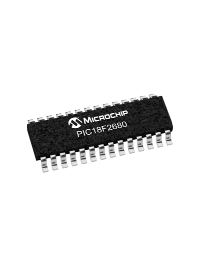
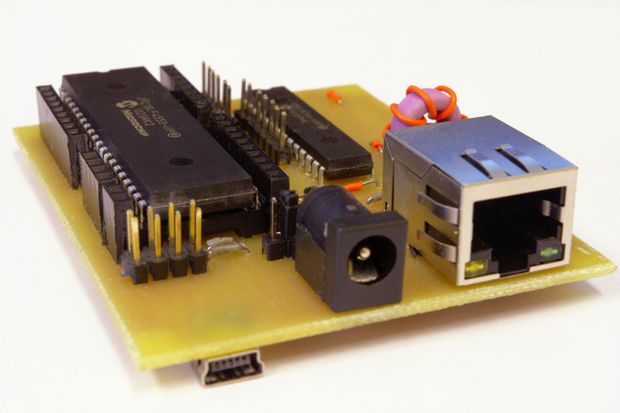
Break PIC18F2680 MCU eeprom memory content can help engineer restore embedded readout-protective firmware from locked PIC18F2680 microcontroller and copy encrypted PIC18F2680 MICROCHIP microprocessor flash program memory binary file or heximal code;
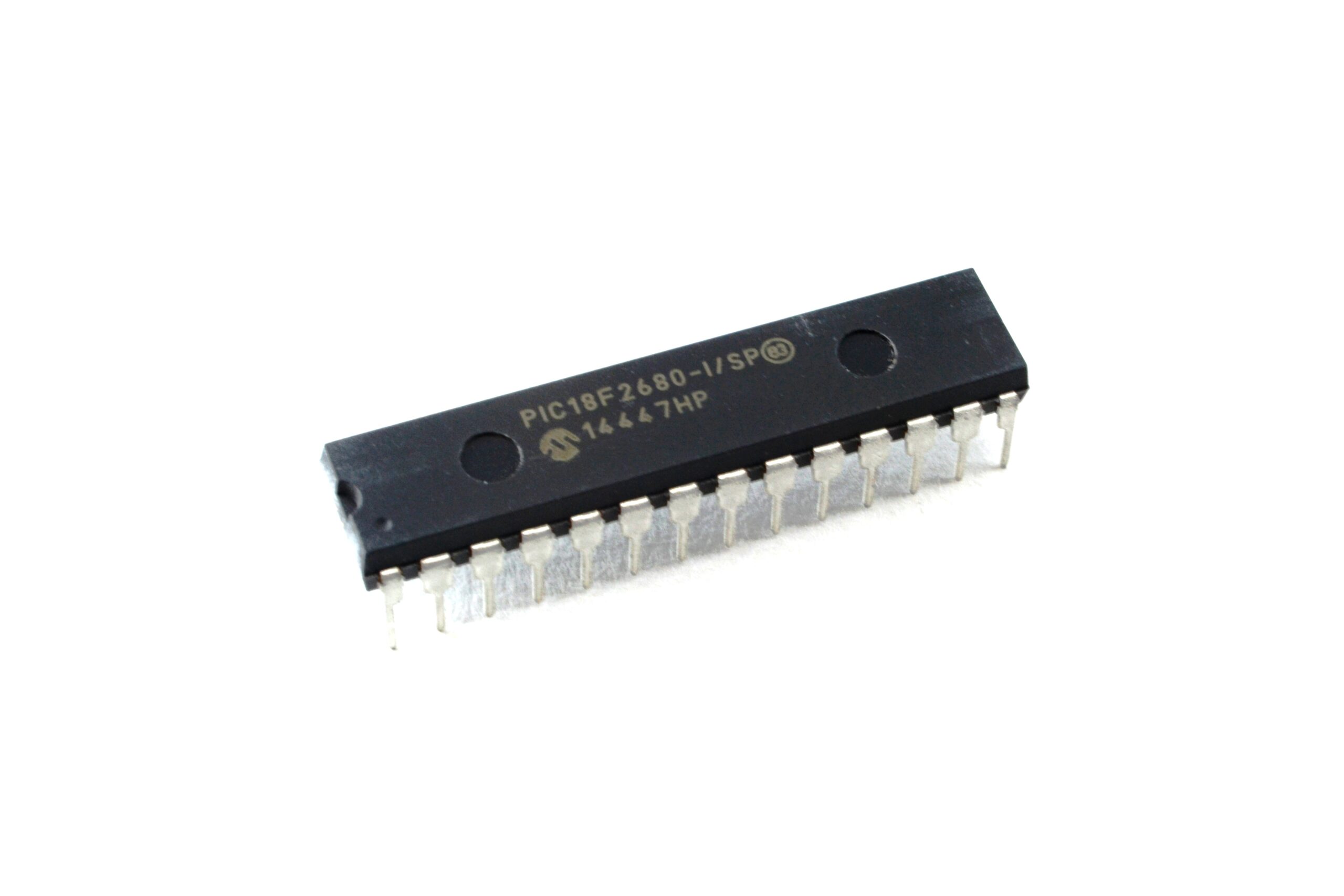
break PIC18F2680 MCU eeprom memory content can help engineer restore embedded readout-protective firmware from locked PIC18F2680 microcontroller and copy encrypted PIC18F2680 MICROCHIP microprocessor flash program memory binary file or heximal code;
This mode is unique among the three low-power Idle modes, in that it does not disable the primary device clock when Break PIC18F2680 MCU Eeprom Memory. For timing sensitive applications, this allows for the fastest resumption of device operation with its more accurate primary clock source, since the clock source does not have to “warm-up” or transition from another oscillator when Recover Locked Chip ATMEGA128PV Binary.
Break PIC18F2680 MCU Eeprom Memory
PRI_IDLE mode is entered from PRI_RUN mode by setting the IDLEN bit and executing a SLEEP instruction when Crack MCU Firmware. If the device is in another Run mode, set IDLEN first, then clear the SCS bits and execute SLEEP to Decrypt Locked MCU ATMEGA128V Embedded Firmware. Although the CPU is disabled, the peripherals continue to be clocked from the primary clock source specified by the FOSC3:FOSC0 Configuration bits. The OSTS bit remains set (see below Figure).
Взлом содержимого памяти EEPROM микроконтроллера PIC18F2680 может помочь инженеру восстановить встроенную защитную прошивку из заблокированного микроконтроллера PIC18F2680 и скопировать зашифрованный двоичный файл или шестнадцатеричный код флэш-памяти микропроцессора PIC18F2680 MICROCHIP;
When a wake event occurs, the CPU is clocked from the primary clock source. A delay of interval TCSD is required between the wake event and when code execution starts. This is required to allow the CPU to become ready to execute instructions. After the wake- up, the OSTS bit remains set. The IDLEN and SCS bits are not affected by the wake-up for the purpose of Dump Microcontroller ATMEGA128V Locked Code (see below Figure).
Złamanie zawartości pamięci EEPROM mikrokontrolera PIC18F2680 może pomóc inżynierowi przywrócić wbudowane oprogramowanie zabezpieczające przed odczytem z zablokowanego mikrokontrolera PIC18F2680 i skopiować zaszyfrowany plik binarny lub kod heksadecymalny pamięci programu mikroprocesora PIC18F2680 MICROCHIP;
The Timer1 oscillator should already be running prior to entering SEC_IDLE mode. If the T1OSCEN bit is not set when the SLEEP instruction is executed, the SLEEP instruction will be ignored and entry to SEC_IDLE mode will not occur through Decrypt Microprocessor ATMEGA169PA Code. If the Timer1 oscillator is enabled but not yet running, peripheral clocks will be delayed until the oscillator has started. In such sit- uations, initial oscillator operation is far from stable and unpredictable operation may result.
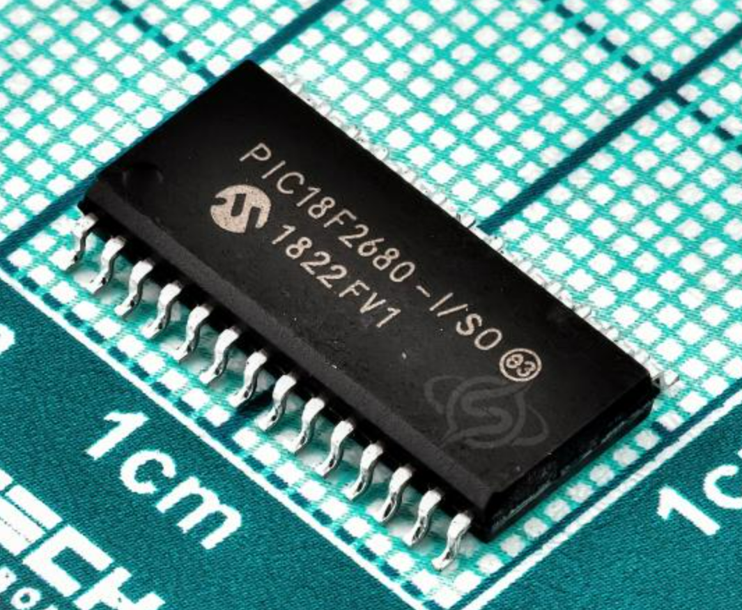
PIC18F2680 MCU eeprom bellek içeriğini kırmak, mühendisin kilitli PIC18F2680 mikrodenetleyicisinden gömülü okuma korumalı aygıt yazılımını geri yüklemesine ve şifrelenmiş PIC18F2680 MICROCHIP mikroişlemci flaş program belleği ikili dosyasını veya onaltılık kodunu kopyalamasına yardımcı olabilir;
Break PIC18F2610 MCU Flash Memory
Break PIC18F2610 MCU flash memory protection and readout embedded firmware in the format of binary data or heximal source code from protective microcontroller PIC18F2610, copy flash memory program or eeprom memory content to new encrypted PIC18F2610 microprocessor;
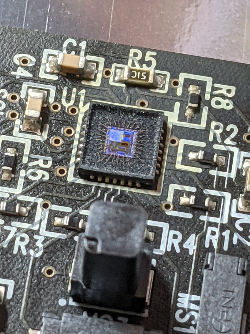
break PIC18F2610 MCU flash memory protection and readout embedded firmware in the format of binary data or heximal source code from protective microcontroller PIC18F2610, copy flash memory program or eeprom memory content to new encrypted PIC18F2610 microprocessor;
The power-managed Sleep mode in the PIC18F2610 devices is identical to the legacy Sleep mode offered in all other PIC devices. It is entered by clearing the IDLEN bit (the default state on device Reset) and executing the SLEEP instruction which faciliate the process of Break PIC18F2610 MCU Flash Memory.
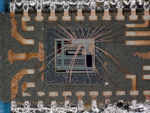
quebrar a proteção de memória flash do MCU PIC18F2610 e ler o firmware incorporado no formato de dados binários ou código-fonte hexadecimal do microcontrolador de proteção PIC18F2610, copiar o programa de memória flash ou o conteúdo da memória eeprom para o novo microprocessador PIC18F2610 criptografado;
This shuts down the selected oscillator (below Figure) after Break IC PIC12F615 Software. All clock source status bits are cleared. Entering the Sleep mode from any other mode does not require a clock switch to Break IC PIC12F635 Program. This is because no clocks are needed once the controller has entered Sleep. If the WDT is selected, the INTRC source will continue to operate. If the Timer1 oscillator is enabled for the purpose of Break IC PIC16F616 Heximal, it will also continue to run.
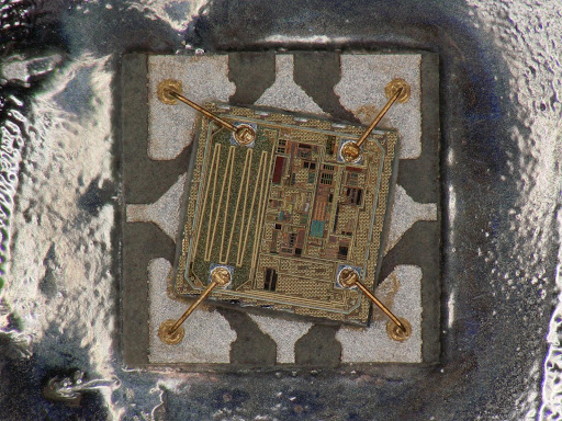
прекъсване на защитата на флаш паметта на PIC18F2610 MCU и вграден фърмуер за четене във формат на двоични данни или шестнадесетичен изходен код от защитен микроконтролер PIC18F2610, копиране на програма за флаш памет или съдържание на eeprom памет към нов криптиран микропроцесор PIC18F2610;
When a wake event occurs in Sleep mode (by interrupt, Reset or WDT time-out), the device will not be clocked until the clock source selected by the SCS1:SCS0 bits becomes ready (see Figure 3-6), or it will be clocked from the internal oscillator block when Break IC PIC12F609 Heximal if either the Two-Speed Start-up or the Fail-Safe Clock Monitor are enabled (see Section 23.0 “Special Features of the CPU”).
PIC18F2610 MCU फ्लैश मेमोरी सुरक्षा को तोड़ना और सुरक्षात्मक माइक्रोकंट्रोलर PIC18F2610 से बाइनरी डेटा या हेक्सिमल स्रोत कोड के प्रारूप में एम्बेडेड फर्मवेयर को पढ़ना, फ्लैश मेमोरी प्रोग्राम या ईप्रोम मेमोरी सामग्री को नए एन्क्रिप्टेड PIC18F2610 माइक्रोप्रोसेसर में कॉपी करना;
In either case, the OSTS bit is set when the primary clock is providing the device clocks. The IDLEN and SCS bits are not affected by the wake-up from Crack MCU Software.
Break PIC18F2610 MCU Flash Memory