Archive for the ‘Break IC’ Category
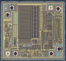
 Break Microchip PIC18F2553 Controller Protection
 August 21st, 2018 |
  Author:
 The power-managed mode that is invoked with the SLEEP instruction is determined by the setting of the IDLEN bit at the time the instruction is executed by Break Microchip PIC18F2553 Controller Protection. If another SLEEP instruction is executed, the device will enter the power-managed mode specified by IDLEN at that time. If IDLEN has changed, the device will enter the new power-managed mode specified by the new setting. Entry to, and exit from Idle mode, does not affect the state of the IDLEN bit.
In the Run modes, clocks to both the core and peripherals are active. The difference between these modes is the clock source. The PRI_RUN mode is the normal, full power execution mode of the microcontroller. This is also the default mode upon a device Reset, unless Two-Speed Start-up is enabled. In this mode, the OSTS bit is set. The IOFS bit may be set if the internal oscillator block is the primary clock source.
Break Microchip PIC18F2553 Controller Protection
The SEC_RUN mode is the compatible mode to the “clock switching” feature offered in other PIC18 devices. In this mode, the CPU and peripherals are clocked from the Timer1 oscillator. This gives users the option of lower power consumption while still using a high accuracy clock source.
SEC_RUN mode is entered by setting the SCS1:SCS0 bits to ‘01’. The device clock source is switched to the Timer1 oscillator (see Figure 3-1), the primary oscillator is shut down, the T1RUN bit (T1CON<6>) is set and the OSTS bit is cleared.
 Posted in
Break PIC18F2523 CPU Memory
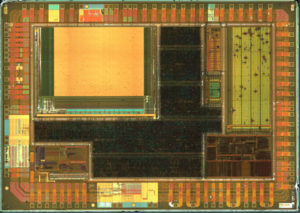
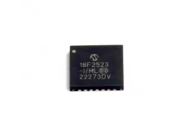
Break PIC18F2523 CPU memory fuse bit and readout protective PIC18F2523 microprocessor program file or data code, secured microcontroller PIC18F2523 embedded firmware can be restored in the format of binary or heximal;
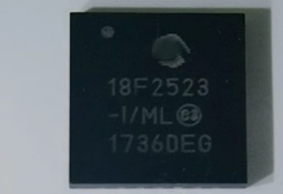
break PIC18F2523 CPU memory fuse bit and readout protective PIC18F2523 microprocessor program file or data code, secured microcontroller PIC18F2523 embedded firmware can be restored in the format of binary or heximal;
A CCP module can use free-running Timer1 (or Timer3), clocked by the internal oscillator block and an external event with a known period to Break PIC18F2523 CPU Memory (i.e., AC power frequency). The time of the first event is captured in the CCPRxH:CCPRxL registers and is recorded for use later. When the second event causes a capture, the time of the first event is subtracted from the time of the second event before Reverse engineering microchip mcu TS87C58X2 locked eeprom. Since the period of the external event is known, the time difference between events can be calculated.
Break PIC18F2523 CPU Memory
If the measured time is much greater than the calculated time, the internal oscillator block is running too fast; to compensate, decrement the OSCTUNE register. If the measured time is much less than the calculated time, the internal oscillator block is running too slow after duplicate avr microprocessor ATMEGA8PA protected firmware; to compensate, increment the OSCTUNE register.
Both timers are cleared, but the timer clocked by the reference generates interrupts. When an interrupt occurs, the internally clocked timer is read and both timers are cleared. If the internally clocked timer value is greater than expected in order to extract atmel microprocessor ATMEGA16PA firmware, then the internal oscillator block is running too fast. To adjust for this, decrement the OSCTUNE register.
كسر فتيل ذاكرة وحدة المعالجة المركزية PIC18F2523 وقراءة ملف برنامج المعالج الدقيق PIC18F2523 أو رمز البيانات، يمكن استعادة البرامج الثابتة المضمنة في وحدة التحكم الدقيقة PIC18F2523 المؤمنة بتنسيق ثنائي أو سداسي عشري؛
Like previous PIC18 devices, the PIC18LF2523 family includes a feature that allows the device clock source to be switched from the main oscillator to an alternate low-frequency clock source. PIC18LF2523 devices offer two alternate clock sources. When an alternate clock source is enabled, the various power-managed operating modes are available for the purpose of reverse engineering ATMEL AVR Chip ATMEGA32A program file.
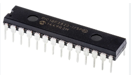
interruzione del fusibile della memoria della CPU PIC18F2523 e lettura del file di programma del microprocessore PIC18F2523 o del codice dati, il firmware incorporato del microcontrollore protetto PIC18F2523 può essere ripristinato nel formato binario o esadecimale;
Essentially, there are three clock sources for these devices:
- Primary oscillators
- Secondary oscillators
- Internal oscillator block
The primary oscillators include the External Crystal and Resonator modes, the External RC modes, the External Clock modes and the internal oscillator block before Crack MCU Software. The particular mode is defined by the FOSC3:FOSC0 Configuration bits.
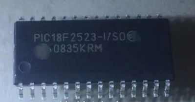
прекъсване на PIC18F2523 CPU предпазител на паметта и защита на четенето PIC18F2523 микропроцесорен програмен файл или код на данни, защитен микроконтролер PIC18F2523 вграден фърмуер може да бъде възстановен във формат на двоичен или шестнадесетичен;
Break PIC18F2510 Microcontroller Flash Memory
Break PIC18F2510 microcontroller flash memory protection and extract embedded firmware from secured PIC18F2510 Microchip MCU flash binary file memory and eeprom heximal data memory, copy source code to new locked microprocessor PIC18F2510;
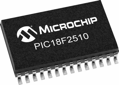
break PIC18F2510 microcontroller flash memory protection and extract embedded firmware from secured PIC18F2510 Microchip MCU flash binary file memory and eeprom heximal data memory, copy source code to new locked microprocessor PIC18F2510;
A Phase Locked Loop (PLL) circuit is provided as an option for users who wish to use a lower frequency oscillator circuit which can be used for Break PIC18F2510 Microcontroller Flash Memory, or to clock the device up to its highest rated frequency from a crystal oscillator. This may be useful for customers who are concerned with EMI due to high-frequency crystals of Protected Winbond Microprocessor W78E65 Reverse Engineering, or users who require higher clock speeds from an internal oscillator.
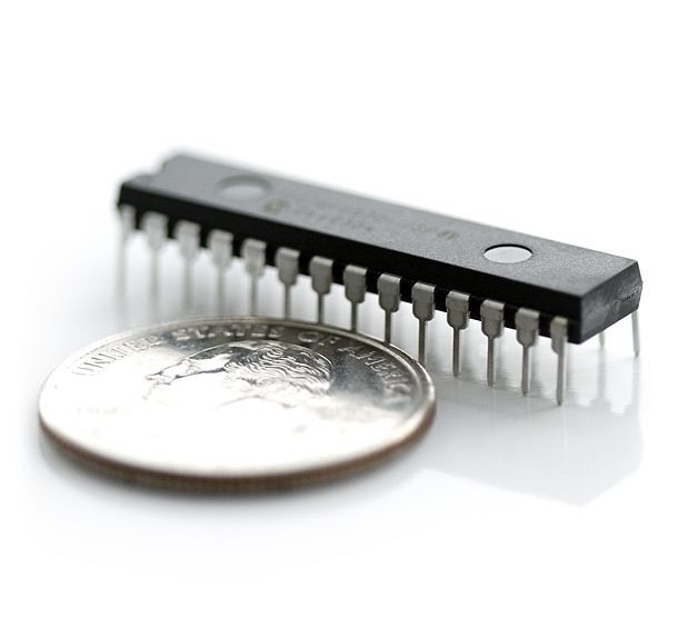
Romper la protección de la memoria flash del microcontrolador PIC18F2510 y extraer el firmware integrado de la memoria de archivo binario flash MCU Microchip PIC18F2510 protegida y la memoria de datos hexagonales EEPROM, copiar el código fuente al nuevo microprocesador PIC18F2510 bloqueado;
The HSPLL mode makes use of the HS mode oscillator for frequencies up to 10 MHz. A PLL then multiplies the oscillator output frequency by 4 to produce an internal clock frequency up to 40 MHz. The PLLEN bit is not available in this oscillator mode after Winbond MCU W78E365 Heximal Data Restoration. The PLL is only available to the crystal oscillator when the FOSC3:FOSC0 Configuration bits are programmed for HSPLL mode (= 0110).
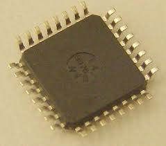
Break PIC18F2510 Microcontroller Flash Memory
The PLL is also available to the internal oscillator block when the INTOSC is configured as the primary clock source. In this configuration, the PLL is enabled in soft- ware and generates a clock output of up to 32 MHz. The operation of INTOSC with the PLL is described in Section 2.6.4 “PLL in INTOSC Modes” after Nuvoton Microcomputer W78E51B Encrypted Heximal Recovery.
The PIC18F2510 devices include an internal oscillator block which generates two different clock signals; either can be used as the microcontroller’s clock source. This may eliminate the need for external oscillator circuits on the OSC1 and/or OSC2 pins.
The main output (INTOSC) is an 8 MHz clock source, which can be used to directly drive the device clock. It also drives a postscaler, which can provide a range of clock frequencies from 31 kHz to 4 MHz. The INTOSC output is enabled when a clock frequency from 125 kHz to 8 MHz is selected, and can provide 31 kHz if required by Attack Nutovon Microcontroller W77E52 Flash Memory.
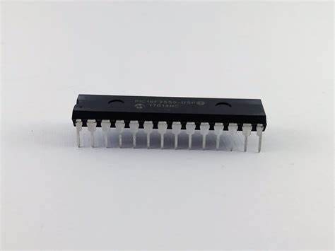
взломать защиту флэш-памяти микроконтроллера PIC18F2510 и извлечь встроенную прошивку из защищенной двоичной файловой флэш-памяти микроконтроллера PIC18F2510 Microchip и шестнадцатеричной памяти данных EEPROM, скопировать исходный код в новый заблокированный микропроцессор PIC18F2510;
The other clock source is the internal RC oscillator (INTRC) which provides a nominal 31 kHz output. INTRC is enabled if it is selected as the device clock source; it is also enabled automatically when any of the following are enabled:
• Power-up Timer
• Fail-Safe Clock Monitor
• Watchdog Timer
These features are discussed in greater detail in Section 23.0 “Special Features of the CPU” after the process of Crack MCU Eeprom. The clock source frequency (INTOSC direct, INTRC direct or INTOSC postscaler) is selected by configuring the IRCF bits of the OSCCON register on Break PIC18F2510 Microcontroller Flash Memory. Additionally, the 31 kHz clock can be provided by either the INTOSC, or INTRC clock sources, depending on the INTSRC bit (OSCTUNE<7>).
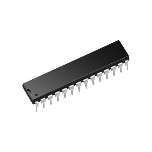
PIC18F2510 마이크로컨트롤러 플래시 메모리 보호를 해제하고 보안된 PIC18F2510 마이크로칩 MCU 플래시 바이너리 파일 메모리와 EEPROM 16진수 데이터 메모리에서 임베디드 펌웨어를 추출하고, 소스 코드를 새로운 잠긴 마이크로프로세서 PIC18F2510에 복사합니다.PIC18F2510 마이크로컨트롤러 플래시 메모리 보호를 해제하고 보안된 PIC18F2510 마이크로칩 MCU 플래시 바이너리 파일 메모리와 EEPROM 16진수 데이터 메모리에서 임베디드 펌웨어를 추출하고, 소스 코드를 새로운 잠긴 마이크로프로세서 PIC18F2510에 복사합니다.
Break PIC18F2450 Microcontroller Locked Heximal
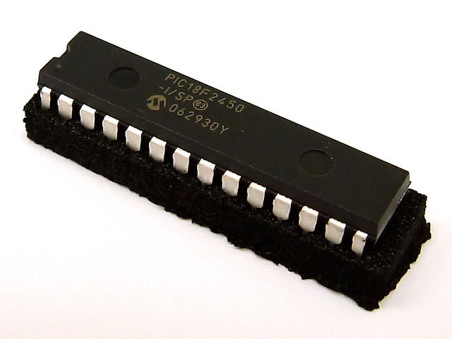
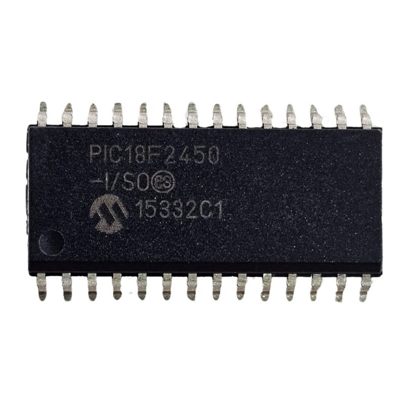
Break PIC18F2450 microcontroller locked heximal is a process start from decrypt secured microprocessor PIC18F2450 fuse bit to recover binary data or heximal file from MICROCHIP PIC18F2450 protective MCU flash program memory and eeprom code memory;
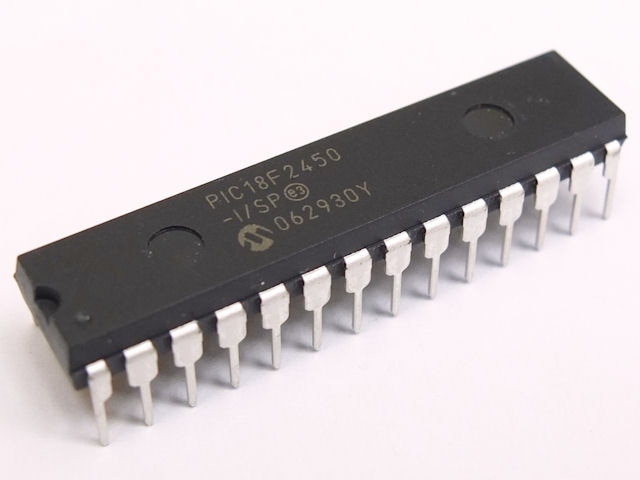
break PIC18F2450 microcontroller locked heximal is a process start from decrypt secured microprocessor PIC18F2450 fuse bit to recover binary data or heximal file from MICROCHIP PIC18F2450 protective MCU flash program memory and eeprom code memory;
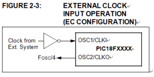
The EC and ECIO Oscillator modes require an external clock source to be connected to the OSC1 pin. There is no oscillator start-up time required after a Power-on Reset or after Break PIC18F2450 Microcontroller Locked Heximal. In the EC Oscillator mode, the oscillator frequency divided by 4 is available on the OSC2 pin. This signal may be used for test purposes or to synchronize other logic. Below Figure shows the pin connections for the EC Oscillator mode.
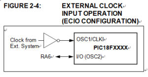
The ECIO Oscillator mode functions like the EC mode, except that the OSC2 pin becomes an additional general purpose I/O pin when Clone IC program. The I/O pin becomes bit 6 of PORTA (RA6). Figure 2-4 shows the pin connections for the ECIO Oscillator mode.
شکستن هگزیمال قفل شده میکروکنترلر PIC18F2450 فرآیندی است که از رمزگشایی ریزپردازنده ایمن بیت فیوز PIC18F2450 برای بازیابی اطلاعات باینری یا فایل هگزیمال از حافظه برنامه فلش محافظ MCU MICROCHIP PIC18F2450 و حافظه کد eeprom شروع می شود.
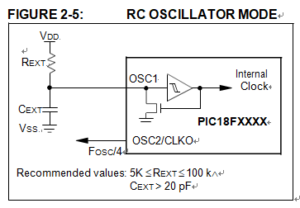
For timing insensitive applications, the “RC” and “RCIO” device options offer additional cost savings. The actual oscillator frequency is a function of several factors:
- supply voltage
- values of the external resistor (REXT) and capacitor (CEXT)
- operating temperature
Break PIC18F2450 Microcontroller Locked Heximal
Given the same device, operating voltage and temperature and component values, there will also be unit-to-unit frequency variations. These are due to factors such as:
PIC18F2450 माइक्रोकंट्रोलर लॉक हेक्सिमल को तोड़ना एक प्रक्रिया है जो डिक्रिप्ट सुरक्षित माइक्रोप्रोसेसर PIC18F2450 फ्यूज बिट से शुरू होती है, जो माइक्रोचिप PIC18F2450 सुरक्षात्मक MCU फ्लैश प्रोग्राम मेमोरी और ईप्रोम कोड मेमोरी से बाइनरी डेटा या हेक्सिमल फ़ाइल को पुनर्प्राप्त करती है;
- normal manufacturing variation
- difference in lead frame capacitance between package types (especially for low CEXT values)
- variations within the tolerance of limits of REXT and CEXT
In the RC Oscillator mode, the oscillator frequency divided by 4 is available on the OSC2 pin. This signal may be used for test purposes or to synchronize other logic. Figure 2-5 shows how the R/C combination is connected.
Взлом заблокированного шестнадцатеричного кода микроконтроллера PIC18F2450 — это процесс, начинающийся с расшифровки защищенного бита предохранителя микропроцессора PIC18F2450 для восстановления двоичных данных или шестнадцатеричного файла из программной флэш-памяти защитного микроконтроллера MICROCHIP PIC18F2450 и памяти кодов EEPROM;
Break PIC18F2423 Protected Memory
Break PIC18F2423 protected memory and recover embedded firmware in the format of binary file or heximal data from secured PIC18F2423 microcontroller by MCU cracking technique,

break PIC18F2423 protected memory and recover embedded firmware in the format of binary file or heximal data from secured PIC18F2423 microcontroller by MCU cracking technique,
In this blog, we explore advanced methods to Break PIC18F2423 microcontroller Protected Memory. We delve into reverse engineering techniques used to access the firmware, recover source code, and extract binary or hexadecimal data from locked microcontroller PIC18F2423. Whether you’re working to restore lost code or break into secured systems for legitimate research, this guide provides insights into the complexities of microprocessor PIC18F2423 security. Learn how to tackle firmware protection, analyze memory layouts, and apply reverse engineering principles to retrieve sensitive information embedded within the chip.

حافظه محافظت شده PIC18F2423 را بشکنید و سیستم عامل تعبیه شده را در قالب فایل باینری یا داده های هگزیمال از میکروکنترلر ایمن PIC18F2423 با تکنیک کرک MCU بازیابی کنید.
NANO Watt technology has been applied on PIC18F2423 Microcontroller which bring much more difficulties in the process of Break PIC18F2423 Protected Memory:
All of the devices in the PIC18F2423 family incorporate a range of features that can significantly reduce power consumption during operation. Key items include:
• Alternate Run Modes: By clocking the controller from the Timer1 source or the internal oscillator block, power consumption during code execution can be reduced by as much as 90% after Recover PIC MCU Microchip 16LF506 Firmware.
• Multiple Idle Modes: The controller can also run with its CPU core disabled but the peripherals still active after Clone IC firmware. In these states, power consumption can be reduced even further, to as little as 4% of normal operation requirements.
• On-the-Fly Mode Switching: The power-managed modes are invoked by user code during operation, allowing the user to incorporate power-saving ideas into their application’s software design before Recover PIC MCU Microchip 12F510 Firmware.
• Low Consumption in Key Modules: The power requirements for both Timer1 and the Watchdog Timer are minimized.
Break PIC18F2423 Protected Memory
All of the devices in the PIC18LF2423 family offer ten different oscillator options, allowing users a wide range of choices in developing application hardware. These include:
• Four Crystal modes, using crystals or ceramic resonators.
• Two External Clock modes, offering the option of using two pins (oscillator input and a divide-by-4 clock output) or one pin (oscillator input, with the second pin reassigned as general I/O).
• Two External RC Oscillator modes with the same pin options as the External Clock modes.
• An internal oscillator block which provides an 8 MHz clock and an INTRC source (approximately 31 kHz) for the purpose of Copy Encrypted Microchip PIC18F2330 Heximal, as well as a range of six user-selectable clock frequencies, between 125 kHz to 4 MHz, for a total of 8 clock frequencies. This option frees the two oscillator pins for use as additional general purpose I/O.
MCU क्रैकिंग तकनीक द्वारा सुरक्षित PIC18F2423 माइक्रोकंट्रोलर से बाइनरी फ़ाइल या हेक्सिमल डेटा के प्रारूप में PIC18F2423 संरक्षित मेमोरी को तोड़ना और एम्बेडेड फर्मवेयर को पुनर्प्राप्त करना,
• A Phase Lock Loop (PLL) frequency multiplier, available to both the High-Speed Crystal and Internal Oscillator modes, which allows clock speeds of up to 40 MHz from the HS clock source. Used with the internal oscillator, the PLL gives users a complete selection of clock speeds when Decrypt Microchip PIC18F2321 MCU Heximal File, from 31 kHz to 32 MHz, all without using an external crystal or clock circuit.
quebrar a memória protegida do PIC18F2423 e recuperar o firmware incorporado no formato de arquivo binário ou dados hexagonais do microcontrolador PIC18F2423 protegido pela técnica de cracking do MCU,
Break AVR MCU ATTINY84 Protected Source Code
In the world of electronics and embedded systems, reverse engineering plays a crucial role in understanding and replicating existing technologies. One of the common challenges faced by professionals and enthusiasts alike is to break AVR MCU ATTINY84 protected source code. This microcontroller, like many others in the AVR family, comes with security measures that prevent unauthorized access to its firmware. These protections are designed to safeguard intellectual property, making it difficult for others to copy or modify the original code. However, individuals with advanced skills in microcontroller and microprocessor systems often attempt to crack this security to access the embedded software.
Reverse engineering of a microcontroller like the ATTINY84 typically involves using sophisticated hardware and software techniques to bypass these protections. These techniques might include analyzing the chip’s physical structure, probing its circuits, or exploiting potential vulnerabilities in the security features. While the practice of cracking protected source code can enable the duplication of proprietary firmware, it often raises ethical and legal concerns, especially when used for unauthorized copying or piracy.
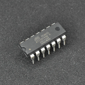
прекъсване на AVR MCU ATtiny84 защитен изходен код от защитена флаш памет и криптирана eeprom памет, възстановяване на изгубен вграден фърмуер на оригиналния микроконтролер ATtiny84 чрез технология за обратно инженерство.
Break AVR MCU ATTINY84 protected source code and extract embedded firmware from secured microcontroller ATTINY84 by binary software or heximal program, copy ATTINY84 encrypted microprocessor content to new MCU;
Break AVR MCU ATTINY84 Protected Source Code
We can break AVR MCU ATTINY84 protected source code, please view the AVR MCU ATTINY84 features for your reference:
The MPLAB SIM Software Simulator allows code development in a PC-hosted environment by simulating the PIC MCUs and dsPIC® DSCs on an instruction level.
On any given instruction, the data areas can be examined or modified and stimuli can be applied from a comprehensive stimulus controller after Break Microcontroller ATMEGA324A Binary. Registers can be logged to files for further run-time analysis.
The trace buffer and logic analyzer display extend the power of the simulator to record and track program execution, actions on I/O, most peripherals and internal registers.
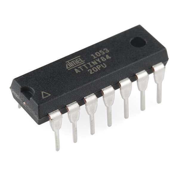
break AVR MCU ATTINY84 protected source code and extract embedded firmware from secured microcontroller ATTINY84 by binary software or heximal program, copy ATTINY84 encrypted microprocessor content to new MCU;
The MPLAB SIM Software Simulator fully supports symbolic debugging using the MPLAB C18 and MPLAB C30 C Compilers, and the MPASM and MPLAB ASM30 Assemblers to provide better support of Reverse engineering IC ATMEGA324PV Code.
The software simulator offers the flexibility to develop and debug code outside of the hardware laboratory environment, making it an excellent, economical software development tool.
The MPLAB ICE 2000 In-Circuit Emulator is intended to provide the product development engineer with a complete AVR MCU design tool set for PIC AVR MCUs. Software control of the MPLAB ICE 2000.
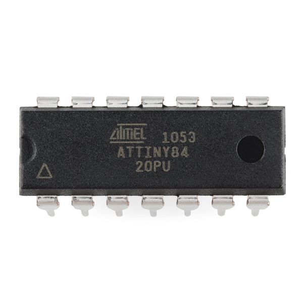
złamać chroniony kod źródłowy mikrokontrolera AVR ATTINY84 i wyodrębnić oprogramowanie sprzętowe z zabezpieczonego mikrokontrolera ATTINY84 za pomocą oprogramowania binarnego lub programu heksametalogowego, skopiować zaszyfrowaną zawartość mikroprocesora ATTINY84 do nowego mikrokontrolera;
In-Circuit Emulator is advanced by the MPLAB Integrated Development Environment, which allows editing, building, downloading and source debugging from a single environment.
The MPLAB ICE 2000 is a full-featured emulator system with enhanced trace to facilitate the progress of Reverse engineering Chip ATMEGA324 Code, trigger and data monitoring features. Interchangeable processor modules allow the system to be easily reconfigured for emulation of different processors.
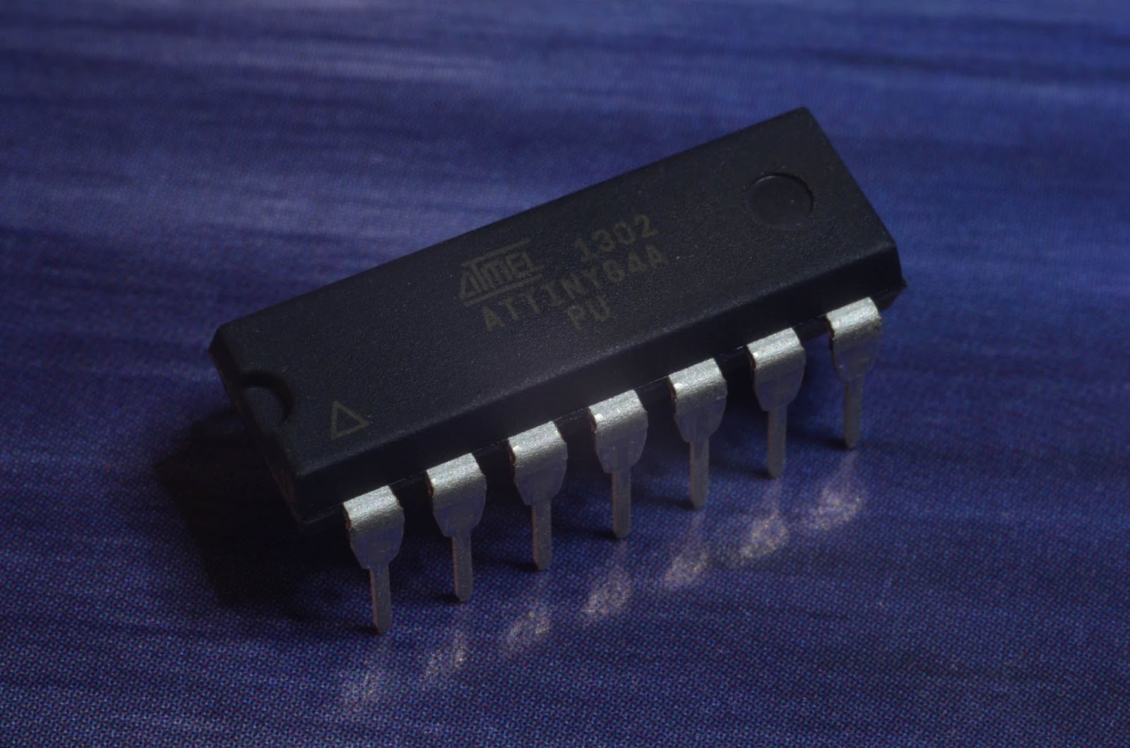
взломать защищенный исходный код микроконтроллера AVR ATTINY84 и извлечь встроенную прошивку из защищенного микроконтроллера ATTINY84 с помощью двоичного программного обеспечения или шестнадцатеричной программы, скопировать зашифрованное содержимое микропроцессора ATTINY84 в новый микроконтроллер;
The architecture of the MPLAB ICE 2000 In-Circuit Emulator allows expansion to support Break Microcontroller ATMEGA164PV Code. The MPLAB ICE 2000 In-Circuit Emulator system has been designed as a real-time emulation system with advanced features that are typically found on more expensive development tools.
The PC platform and Microsoft® Windows® 32-bit operating system were chosen to best make these features available in a simple, unified application by Crack MCU Program.
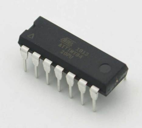
बाइनरी सॉफ्टवेयर या हेक्सिमल प्रोग्राम द्वारा AVR MCU ATTINY84 संरक्षित स्रोत कोड को तोड़ना और सुरक्षित माइक्रोकंट्रोलर ATTINY84 से एम्बेडेड फर्मवेयर निकालना, ATTINY84 एन्क्रिप्टेड माइक्रोप्रोसेसर सामग्री को नए MCU में कॉपी करना;
Break Chip ATMEGA861P Code
Break chip ATMEGA861P code and read embedded firmware from original secured microprocessor ATMEGA861P out from flash program memory and eeprom data memory, reverse engineering protective microcontroller ATMEGA861P can help engieer to clone the full functions of protective ATMEGA861P microcontroller;
Break Chip ATMEGA861P Code
Timer 2 is selected as the baud rate generator by setting TCLK and/or RCLK in T2CON (Table 2). Note that the baud rates for transmit and receive can be different if Timer 2 is used for the receiver or transmitter and Timer 1 is used for the other function. Setting RCLK and/or TCLK puts Timer 2 into its baud rate generator mode, as shown in Figure 4 when Break Chip ATMEGA861P Code.
The baud rate generator mode is similar to the auto-reload mode, in that a rollover in TH2 causes the Timer 2 registers to be reloaded with the 16 bit value in registers RCAP2H and RCAP2L, which are preset by Copy IC PIC16LF877 Program.
The baud rates in Modes 1 and 3 are determined by Timer 2’s overflow rate according to the following equation. The Timer can be configured for either timer or counter operation. In most applications, it is configured for timer operation (CP/T2 = 0).
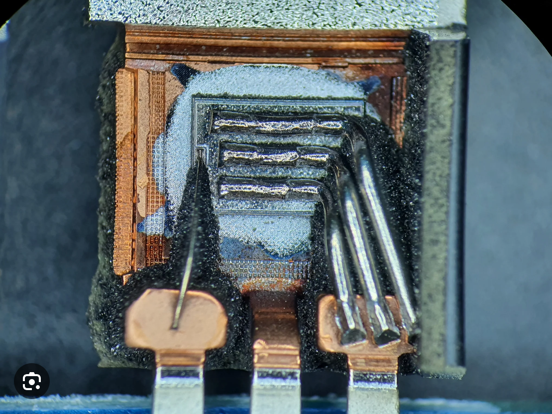
break chip ATMEGA861P code and read embedded firmware from original secured microprocessor ATMEGA861P out from flash program memory and eeprom data memory, reverse engineering protective microcontroller ATMEGA861P can help engieer to clone the full functions of protective ATMEGA861P microcontroller;
The timer operation is different for Timer 2 when it is used as a baud rate generator. Normally, as a timer, it increments every machine cycle (at 1/12 the oscillator frequency). As a baud rate generator, however, it increments every state time (at 1/2 the oscillator fre-quency) to facilitate the progress of Attack Chip ST62T00CB6 Firmware.
The baud rate formula is given below. where (RCAP2H, RCAP2L) is the content of RCAP2H and RCAP2L taken as a 16 bit unsigned integer.
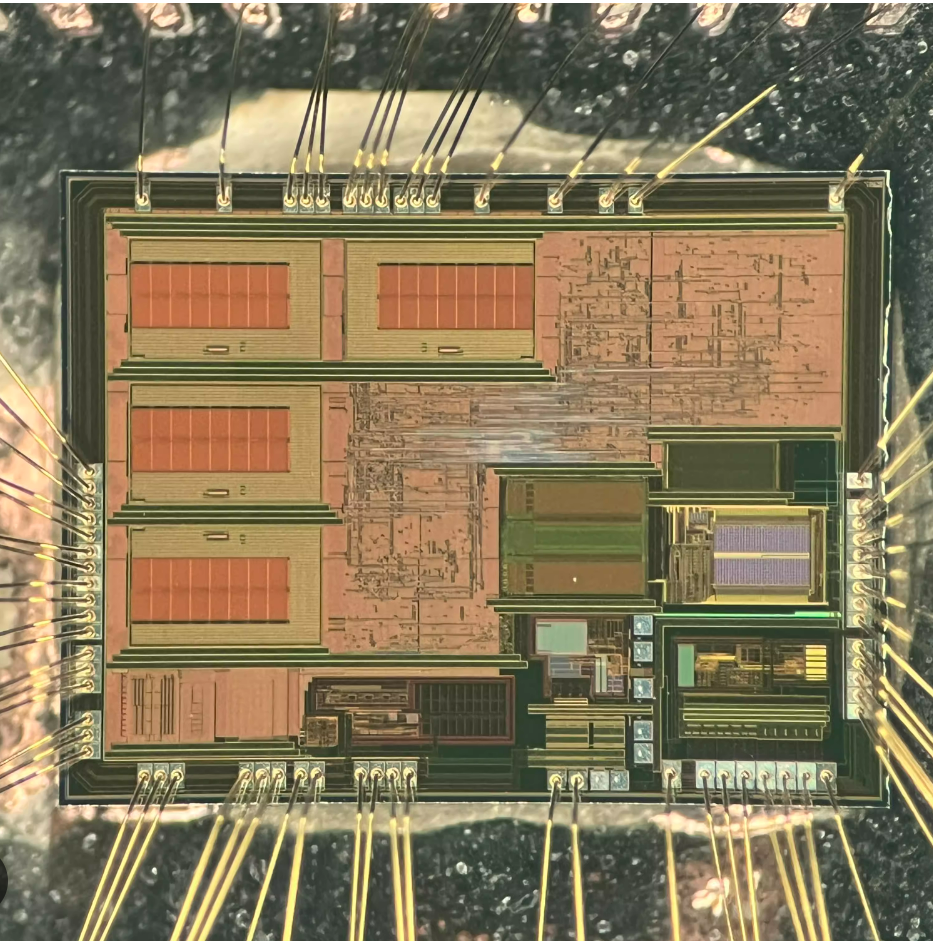
złamanie kodu układu scalonego ATMEGA861P i odczytanie wbudowanego oprogramowania układowego z oryginalnego zabezpieczonego mikroprocesora ATMEGA861P z pamięci programu flash i pamięci danych eeprom; inżynieria wsteczna ochronnego mikrokontrolera ATMEGA861P może pomóc inżynierowi sklonować pełne funkcje ochronnego mikrokontrolera ATMEGA861P;
This figure is valid only if RCLK or TCLK = 1 in T2CON. Note that a rollover in TH2 does not set TF2 and will not generate an interrupt. Note too, that if EXEN2 is set, a 1-to-0 transition in T2EX will set EXF2 but will not cause a reload from (RCAP2H, RCAP2L) to (TH2, TL2) to better support the progress of Attack Microcontroller MC68HC705P6ACDW Binary.
Thus when Timer 2 is in use as a baud rate generator, T2EX can be used as an extra external interrupt. Note that when Timer 2 is running (TR2 = 1) as a timer in the baud rate generator mode, TH2 or TL2 should not be read from or written to Attack MCU TMX320F28027PTA Archive.
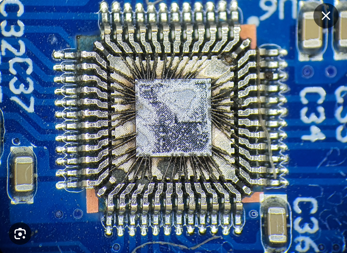
взломать код чипа ATMEGA861P и считать встроенную прошивку оригинального защищенного микропроцессора ATMEGA861P из флэш-памяти программ и памяти данных EEPROM, обратная разработка защитного микроконтроллера ATMEGA861P может помочь инженеру клонировать все функции защитного микроконтроллера ATMEGA861P;
Under these conditions, the Timer is incremented every state time, and the results of a read or write may not be accurate. The RCAP2 registers may be read but should not be written to, because a write might overlap a reload and cause write and/or reload errors. The timer should be turned off (clear TR2) before accessing the Timer 2 or RCAP2 registers after Unlock Microcontroller Memory.
ATMEGA861P चिप कोड को तोड़ें और मूल सुरक्षित माइक्रोप्रोसेसर ATMEGA861P से एम्बेडेड फर्मवेयर को फ्लैश प्रोग्राम मेमोरी और ईप्रोम डेटा मेमोरी से पढ़ें, रिवर्स इंजीनियरिंग सुरक्षात्मक माइक्रोकंट्रोलर ATMEGA861P, सुरक्षात्मक ATMEGA861P माइक्रोकंट्रोलर के पूर्ण कार्यों को क्लोन करने के लिए इंजीनियर की मदद कर सकता है;
Break MCU ATMEGA861V Flash
Breaking MCU ATMEGA861V Flash involves a complex process of reverse engineering, often aimed at bypassing the security mechanisms protecting the firmware stored in ATMEGA861V microcontroller. This process requires advanced knowledge of microprocessors and embedded systems. The goal is to crack the protections of ATMEGA861V and decrypt the firmware, allowing access to the binary or hexadecimal code that controls the MCU’s functions. By decoding this protected data, engineers can copy, modify, or analyze the underlying software.
Breaking MCU ATMEGA861V Flash involves a complex process of reverse engineering, often aimed at bypassing the security mechanisms protecting the firmware stored in ATMEGA861V microcontroller. This process requires advanced knowledge of microprocessors and embedded systems. The goal is to crack the protections of ATMEGA861V and decrypt the firmware, allowing access to the binary or hexadecimal code that controls the MCU’s functions. By decoding this protected data, engineers can copy, modify, or analyze the underlying software.
Microcontrollers like the ATMEGA861V are designed with safeguards to prevent unauthorized access to their internal flash memory, which stores crucial firmware. However, reverse engineering experts use sophisticated techniques to decrypt and decode this data, exposing the microcontroller’s inner workings. This involves analyzing the binary and hexadecimal representation of the code to understand its behavior and structure.
While the intention behind breaking MCU flash memory can range from system recovery to creating compatible hardware, the ethical implications remain significant. Unauthorized copying or modification of firmware can infringe on intellectual property rights, so the process of breaking MCU ATMEGA861V Flash should be approached with care, considering both the technical challenges and legal boundaries.
Break MCU ATMEGA861V Flash
A 50% duty cycle clock can be programmed to come out on P1.0, as shown in above Figure. This pin, besides being a regular I/0 pin, has two alternate functions when Attack IC ADUC831BSZ Firmware. It can be programmed to input the external clock for Timer/Counter 2 or to output a 50% duty cycle clock ranging from 61 Hz to 4 MHz at a 16 MHz operating frequency.
To configure the Timer/Counter 2 as a clock generator, bit C/T2 (T2CON.1) must be cleared and bit T2OE (T2MOD.1) must be set. Bit TR2 (T2CON.2) starts and stops the timer.
The clock-out frequency depends on the oscillator frequency and the reload value of Timer 2 capture registers (RCAP2H, RCAP2L) in order to Break MCU AT89C5131A Binary, as shown in the following equation.
In the clock-out mode, Timer 2 rollovers will not generate an interrupt. This behavior is similar to when Timer 2 is used as a baud-rate generator in order to Break Chip PIC16F720 Firmware. It is possible to use Timer 2 as a baud-rate generator and a clock generator simultaneously.
MCU ATMEGA861V फ्लैश को तोड़ने में रिवर्स इंजीनियरिंग की एक जटिल प्रक्रिया शामिल होती है, जिसका उद्देश्य अक्सर ATMEGA861V माइक्रोकंट्रोलर में संग्रहीत फर्मवेयर की सुरक्षा करने वाले सुरक्षा तंत्र को बायपास करना होता है। इस प्रक्रिया के लिए माइक्रोप्रोसेसर और एम्बेडेड सिस्टम के उन्नत ज्ञान की आवश्यकता होती है। इसका लक्ष्य ATMEGA861V की सुरक्षा को तोड़ना और फर्मवेयर को डिक्रिप्ट करना है, जिससे MCU के कार्यों को नियंत्रित करने वाले बाइनरी या हेक्साडेसिमल कोड तक पहुँच प्राप्त हो सके। इस संरक्षित डेटा को डिकोड करके, इंजीनियर अंतर्निहित सॉफ़्टवेयर की प्रतिलिपि बना सकते हैं, उसे संशोधित कर सकते हैं या उसका विश्लेषण कर सकते हैं।
Note, however, that the baud-rate and clock-out frequencies cannot be determined independently from one another since they both use RCAP2H and RCAP2L when break MCU flash.
The UART in the ATmega861v operates the same way as the UART in IC Cloning. For further information, see the October 1995 MMCUrocontroller Data Book, page 2-49, section titled, “Serial Interface.”
The serial peripheral interface (SPI) allows high-speed synchronous data transfer when Break Microcontroller PIC16F767 Firmware between the ATMEGA861V and peripheral devMCUes or between several ATMEGA861V devMCUes.
The ATmega861V SPI features include the following:
Full-Duplex, 3-Wire Synchronous Data Transfer
Master or Slave Operation
1.5-MHz Bit Frequency (max.)
LSB First or MSB First Data Transfer
Four Programmable Bit Rates
End of Transmission Interrupt Flag
Write Collision Flag Protection
Wakeup from Idle Mode (Slave Mode Only)
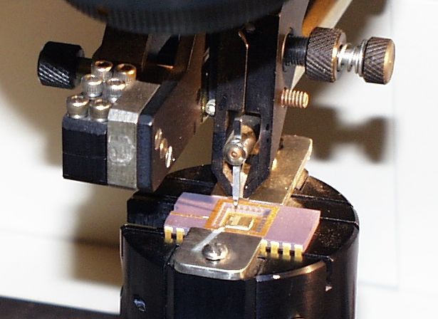
شکستن فلش MCU ATMEGA861V شامل یک فرآیند پیچیده مهندسی معکوس است که اغلب با هدف دور زدن مکانیسم های امنیتی محافظت از سیستم عامل ذخیره شده در میکروکنترلر ATMEGA861V انجام می شود. این فرآیند نیازمند دانش پیشرفته ریزپردازنده ها و سیستم های تعبیه شده است. هدف این است که حفاظت ATMEGA861V را شکسته و سفتافزار را رمزگشایی کند تا به کد باینری یا هگزادسیمال که عملکردهای MCU را کنترل میکند، دسترسی داشته باشید. با رمزگشایی این داده های محافظت شده، مهندسان می توانند نرم افزار زیربنایی را کپی، اصلاح یا تجزیه و تحلیل کنند.
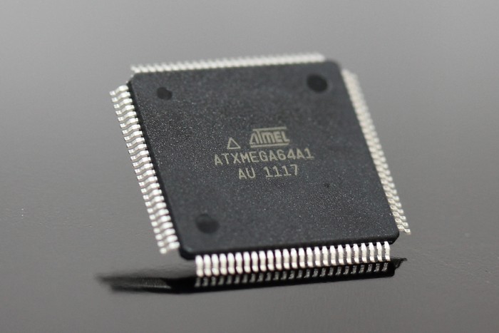
Break MCU ATXMEGA64A1 Heximal
Breaking MCU ATXMEGA64A1 Heximal often involves reverse engineering and decrypting its firmware to access flash memory, EEPROM, or binary code. By analyzing the program’s heximal and binary format, it’s possible to recover, restore, copy, or clone essential software or source code for diagnostics and backup purposes.
Breaking MCU ATXMEGA64A1 Heximal often involves reverse engineering and decrypting its firmware to access flash memory, EEPROM, or binary code. By analyzing the program’s heximal and binary format, it’s possible to recover, restore, copy, or clone essential software or source code for diagnostics and backup purposes
The AVR architecture has two main memory spaces, the Program Memory and the Data Memory. In addition, the XMEGA A1 features an EEPROM Memory for non-volatile data storage after Break MCU ATXMEGA64A1 Heximal.
All three memory spaces are linear and require no paging. The available memory size configurations are shown in “Ordering Information”. In addition each device has a Flash memory signature row for calibration data after Break Microcontroller Samsung S3F9454 Software, device identification, serial number etc. Non-volatile memory spaces can be locked for further write or read/write operations.
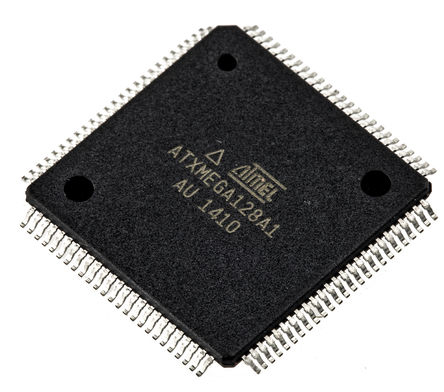
la rottura di MCU ATXMEGA64A1 Heximal spesso comporta il reverse engineering e la decifrazione del suo firmware per accedere alla memoria flash, EEPROM o codice binario. Analizzando il formato esadecimale e binario del programma, è possibile recuperare, ripristinare, copiare o clonare software essenziale o codice sorgente per scopi di diagnostica e backup
This prevents unrestricted access to the application software. When the device is powered on, the CPU starts to execute instructions from the lowest address in the Flash Program Memory ‘0’. The Program Counter (PC) addresses the next instruction to be fetched. After a reset, the PC is set to location ‘0’ from MCU Cracking.
Program flow is provided by conditional and unconditional jump and call instructions in order to Break Microcontroller NEC UPD78F0881 Software, capable of addressing the whole address space directly. Most AVR instructions use a 16-bit word format, while a limited number uses a 32-bit format.
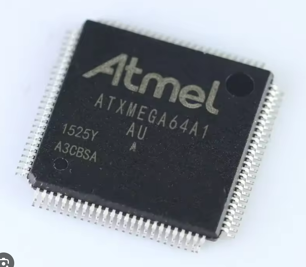
غالبًا ما يتضمن كسر MCU ATXMEGA64A1 Heximal الهندسة العكسية وفك تشفير البرامج الثابتة للوصول إلى ذاكرة الفلاش أو EEPROM أو الكود الثنائي. من خلال تحليل تنسيق البرنامج السداسي والثنائي، من الممكن استرداد أو استعادة أو نسخ أو استنساخ البرامج الأساسية أو الكود المصدر لأغراض التشخيص والنسخ الاحتياطي
During interrupts and subroutine calls, the return address PC is stored on the Stack. The Stack is effectively allocated in the general data SRAM, and consequently the Stack size is only limited by the total SRAM size and the usage of the SRAM.
After reset the Stack Pointer (SP) points to the highest address in the internal SRAM. The SP is read/write accessible in the I/O memory space, enabling easy implementation of multiple stacks or stack areas for the purpose of Break Microcontroller TI MSP430F448 Firmware. The data SRAM can easily be accessed through the five different addressing modes supported in the AVR CPU.
• Flash Program Memory
– One linear address space
– In-System Programmable
– Self-Programming and Bootloader support
– Application Section for application code
– Application Table Section for application code or data storage
– Boot Section for application code or bootloader code
– Separate lock bits and protection for all sections
• Data Memory
– One linear address space
– Single cycle access from CPU
– SRAM
– EEPROM
Byte or page accessible
Optional memory mapping for direct load and store
– I/O Memory
Configuration and Status registers for all peripherals and modules
16-bit accessible General Purpose Register for global variables or flags
– External Memory support
– Bus arbitration
Safe and deterministic handling of CPU and DMA Controller priority
– Separate buses for SRAM, EEPROM, I/O Memory and External Memory access
Simultaneous bus access for CPU and DMA Controller
• Calibration Row Memory for factory programmed data
Oscillator calibration bytes
Serial number
Device ID for each device type
• User Signature Row
One flash page in size
Can be read and written from software
Data is kept
злам мікроконтроллера ATXMEGA64A1 Heximal часто передбачає зворотне проектування та розшифровку мікропрограми для доступу до флеш-пам’яті, EEPROM або двійкового коду. Аналізуючи шістнадцятковий і двійковий формати програми, можна відновити, відновити, скопіювати або клонувати важливе програмне забезпечення або вихідний код для діагностики та резервного копіювання.
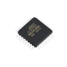
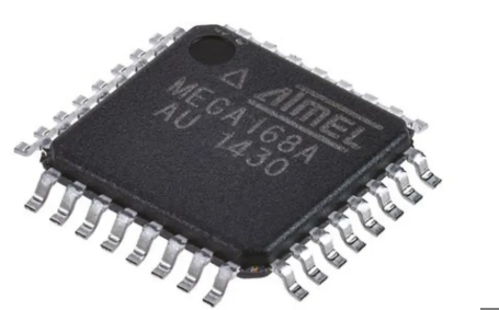
Break MCU ATmega168A Flash
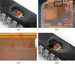
Breaking MCU ATmega168A flash involves cracking the encrypted and locked firmware to access the program and source code embedded within its secured flash memory and EEPROM memory. This protective microcontroller (MCU) is designed to safeguard its binary and heximal data against unauthorized access. However, reverse engineering techniques can be employed to decode and unlock its secured firmware for legitimate purposes such as system restoration or hardware cloning.
Quebrar o flash MCU ATmega168A envolve quebrar o firmware criptografado e bloqueado para acessar o programa e o código-fonte embutidos em sua memória flash segura e memória EEPROM. Este microcontrolador de proteção (MCU) é projetado para proteger seus dados binários e hexagonais contra acesso não autorizado. No entanto, técnicas de engenharia reversa podem ser empregadas para decodificar e desbloquear seu firmware seguro para fins legítimos, como restauração do sistema ou clonagem de hardware.
The process requires an in-depth understanding of the microprocessor’s architecture to bypass security features and retrieve the embedded software. Advanced tools are used to extract and decode the encrypted data stored in the flash memory. Once unlocked, the firmware can be restored to its original functionality or cloned for replication in similar systems.
While breaking the ATmega168A’s flash provides a solution for restoring or replicating old or damaged microcomputers, it must be performed within ethical and legal boundaries to ensure intellectual property rights are respected.
Break MCU ATmega168A Flash
Most of the instructions operating on the Register File have direct access to all registers, and most of them are single cycle instructions. Each register is also assigned a data memory address, mapping them directly into the first 32 locations of the user Data Space. Although not being physically implemented as SRAM locations, this memory organization provides great flexibility in access of the registers which is useful for Break MCU ATmega168A Flash, as the X-, Y- and Z-pointer registers can be set to index any register in the file. The registers R26..R31 have some added functions to their general purpose usage.
These registers are 16-bit address pointers for indirect addressing of the data space. The Stack is mainly used for storing temporary data, for storing local variables and for storing return addresses after interrupts and subroutine calls.
MCU ATmega168A flaşını kırmak, güvenli flaş belleği ve EEPROM belleğinde gömülü programa ve kaynak koduna erişmek için şifrelenmiş ve kilitlenmiş aygıt yazılımını kırmayı içerir. Bu koruyucu mikrodenetleyici (MCU), ikili ve heksimal verilerini yetkisiz erişime karşı korumak için tasarlanmıştır. Ancak, tersine mühendislik teknikleri, sistem geri yükleme veya donanım klonlama gibi meşru amaçlar için güvenli aygıt yazılımını çözmek ve kilidini açmak için kullanılabilir.
The Stack Pointer Register always points to the top of the Stack. Note that the Stack is implemented as growing from higher memory locations to lower memory locations. This implies that a Stack PUSH command decreases the Stack Pointer by Hack IC firmware. The Stack Pointer points to the data SRAM Stack area where the Subroutine and Interrupt Stacks are located. This Stack space in the data SRAM must be defined by the program before any subroutine calls are executed or interrupts are enabled.
The Stack Pointer must be set to point above 0x0100, preferably RAMEND. The Stack Pointer is decremented by one when data is pushed onto the Stack with the PUSH instruction, and it is decremented by two when the return address is pushed onto the Stack with subroutine call or interrupt.
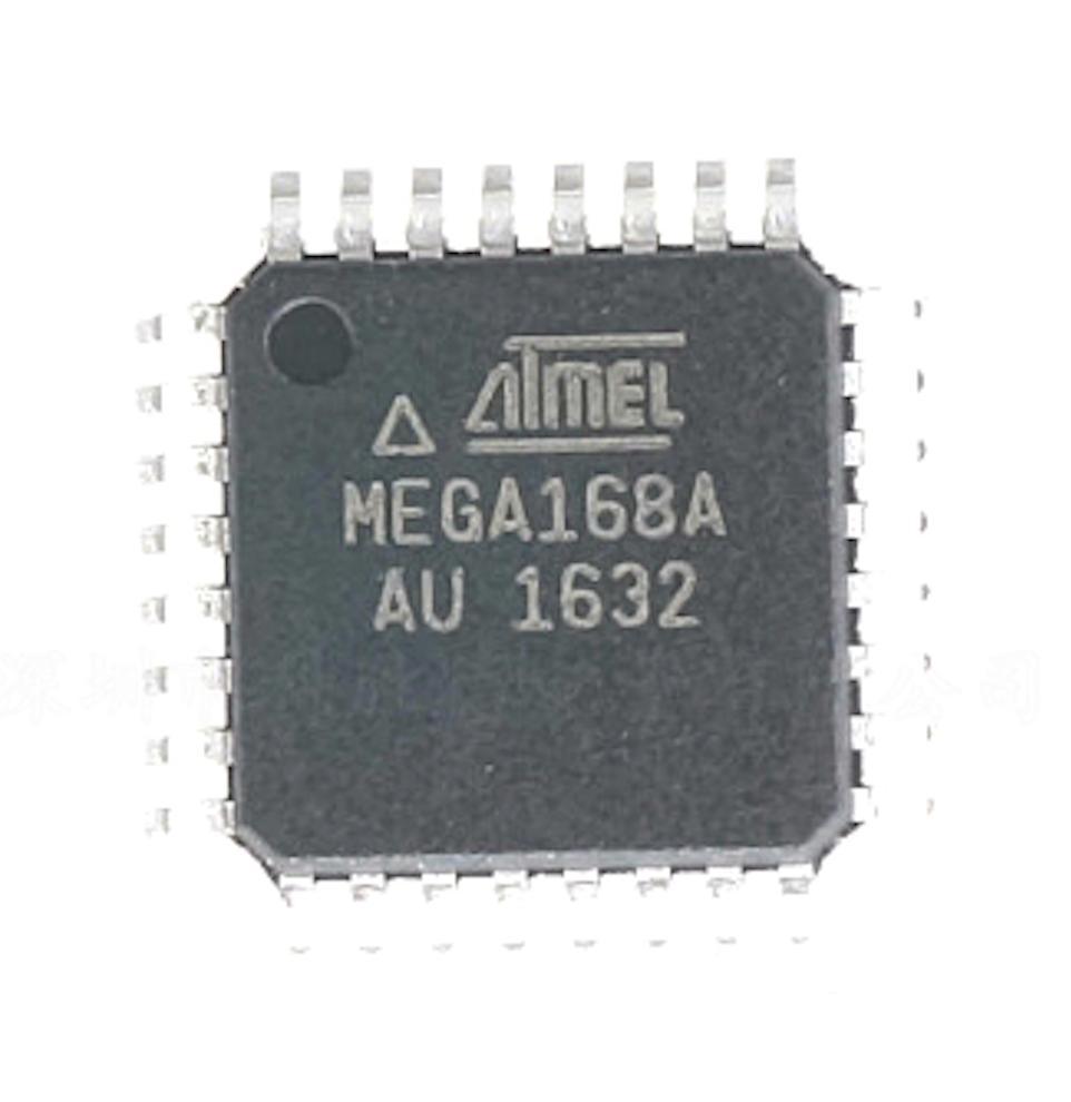
recover embedded firmware from atmega168a mcu flash memory
The Stack Pointer is incremented by one when data is popped from the Stack with the POP instruction, and it is incremented by two when data is popped from the Stack with return from subroutine RET or return from interrupt RETI.
The AVR Stack Pointer is implemented as two 8-bit registers in the I/O space. The number of bits actually used is implementation dependent. Note that the data space in some implementations of the AVR architecture is so small that only SPL is needed. In this case, the SPH Register will not be present after Extract MCU Firmware.
This section describes the general access timing concepts for instruction execution. The AVR CPU is driven by the CPU clock clkCPU, directly generated from the selected clock source for the MCU Cracking. No internal clock division is used.
Figure 5-4 shows the parallel instruction fetches and instruction executions enabled by the Harvard architecture and the fast-access Register File concept. This is the basic pipelining concept to obtain up to 1 MIPS per MHz with the corresponding unique results for functions per cost, functions per clocks, and functions per power-unit.
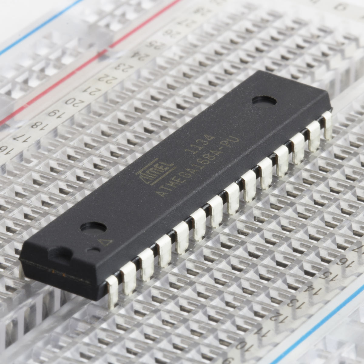
break ATMEGA168A secured microprocessor fuse bit and readout embedded program from flash memory and data from eeprom memory
The AVR provides several different interrupt sources. These interrupts and the separate Reset Vector each have a separate program vector in the program memory space. All interrupts are assigned individual enable bits which must be written logic one together with the Global Interrupt Enable bit in the Status Register in order to enable the interruption in the process of Break MCU ATmega168A Flash. Depending on the Program Counter value, interrupts may be automatically disabled when Boot Lock bits BLB02 or BLB12 are programmed. This feature improves software security. See the section ”Memory Programming” on page 285 for details.
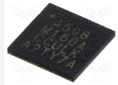
Взлом флэш-памяти MCU ATmega168A включает взлом зашифрованной и заблокированной прошивки для доступа к программе и исходному коду, встроенному в защищенную флэш-память и память EEPROM. Этот защитный микроконтроллер (MCU) предназначен для защиты своих двоичных и шестнадцатеричных данных от несанкционированного доступа. Однако методы обратного проектирования могут быть использованы для декодирования и разблокировки его защищенной прошивки в законных целях, таких как восстановление системы или клонирование оборудования.