 Reverse Engineering Chip ATmega644A Code
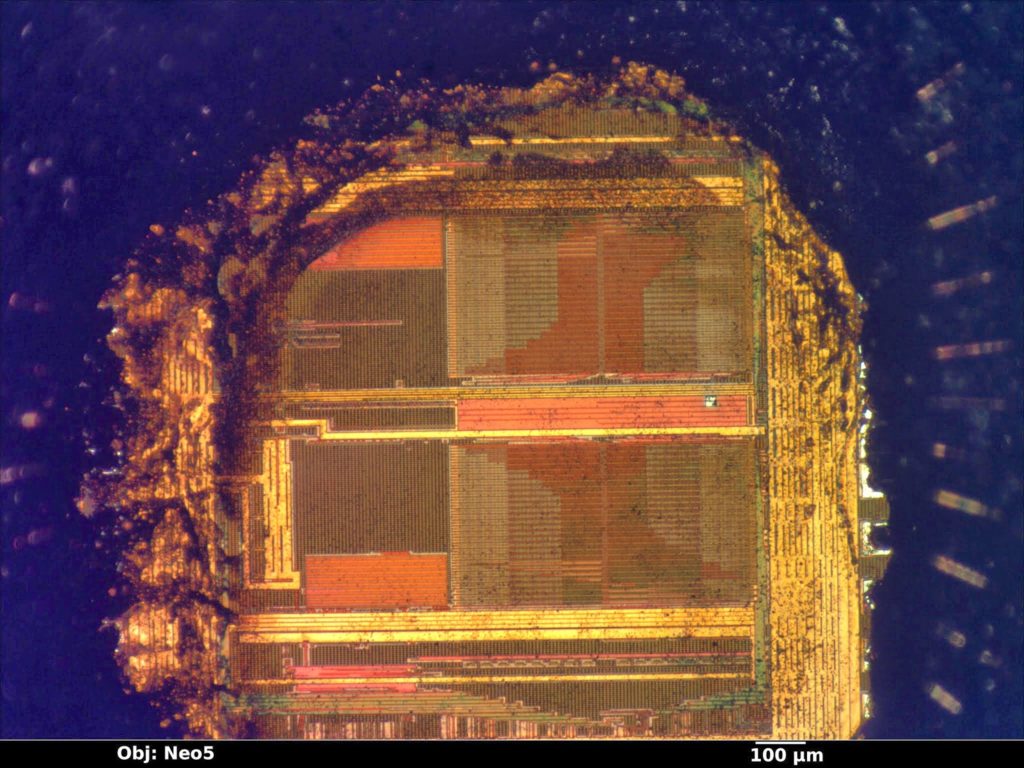
Reverse Engineering Chip ATmega644A and extract microcontroller scheme to locate the security fuse bit of embedded flash, cut it off by breaking MCU technique, read processor atmega644a code and make new microprocessor cloning;
When the SM2..0 bits are written to 000, the SLEEP instruction makes the Chip enter Idle mode, stopping the CPU but allowing the SPI, USART, Analog Comparator, ADC, 2-wire Serial Interface, Timer/Counters, Watchdog, and the interrupt system to continue operating. This sleep mode basically halts clkCPU and clkFLASH, while allowing the other clocks to run. Idle mode enables the Chip to wake up from external triggered interrupts as well as internal ones like the Timer Overflow and USART Transmit Complete interrupts.
If wake-up from the Analog Comparator interrupt is not required, the Analog Comparator can be powered down by setting the ACD bit in the Analog Comparator Control and Status Register – ACSR. This will reduce power consumption in Idle mode. If the ADC is enabled, a conversion starts automatically when this mode is entered before attack mcu protection.
When the SM2..0 bits are written to 001, the SLEEP instruction makes the Chip enter ADC Noise Reduction mode, stopping the CPU but allowing the ADC, the external interrupts, 2-wire Serial Interface address match, Timer/Counter2 and the Watchdog to continue operating (if enabled). This sleep mode basically halts clkI/O, clkCPU, and clk-FLASH, while allowing the other clocks to run.
This improves the noise environment for the ADC, enabling higher resolution measurements. If the ADC is enabled, a conversion starts automatically when this mode is entered when Reverse Engineering Chip code.
Apart form the ADC Conversion Complete interrupt, only an External Reset, a Watchdog System Reset, a Watchdog interrupt, a Brown-out Reset, a 2-wire serial interface interrupt, a Timer/Counter2 interrupt, an SPM/EEPROM ready interrupt, an external level interrupt on INT7:4 or a pin change interrupt can wakeup the Chip from ADC Noise Reduction mode.
When the SM2..0 bits are written to 010, the SLEEP instruction makes the Chip enter Power-down mode. In this mode, the external Oscillator is stopped, while the external interrupts, the 2-wire Serial Interface, and the Watchdog continue operating (if enabled).
Only an External Reset, a Watchdog Reset, a Brown-out Reset, 2-wire Serial Interface address match, an external level interrupt on INT7:4, an external interrupt on INT3:0, or a pin change interrupt can wake up the Chip. This sleep mode basically halts all generated clocks, allowing operation of asynchronous modules only after Reverse Engineering MICROCONTROLLER.