 Break MCU ATmega1280PV Code
 January 26th, 2010 |
  Author:
 Break MCU ATmega1280PV Code can help engineer to recover embedded firmware such as heximal from flash memory and atmega128 microcontroller;
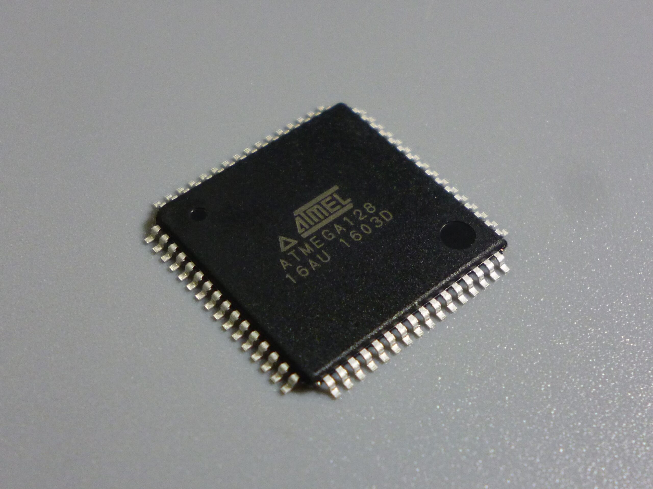
Break MCU ATmega1280PV Code can help engineer to recover embedded firmware such as heximal from flash memory and atmega128 microcontroller;
The FOC0A bit is only active when the WGM bits specify a non-PWM mode. However, for ensuring compatibility with future devices, this bit must be set to zero when TCCR0B is written when operating in PWM mode.
When writing a logical one to the FOC0A bit, an immediate Compare Match is forced on the Waveform Generation unit.
The OC0A output is changed according to its COM0A1:0 bits setting. Note that the FOC0A bit is implemented as a strobe. Therefore it is the value present in the COM0A1:0 bits that determines the effect of the forced compare. A FOC0A strobe will not generate any interrupt, nor will it clear the timer in CTC mode using OCR0A as TOP in the process of breaking off atmega128 microcontroller protection. The FOC0A bit is always read as zero. The FOC0B bit is only active when the WGM bits specify a non-PWM mode.
However, for ensuring compatibility with future devices, this bit must be set to zero when TCCR0B is written when operating in PWM mode. When writing a logical one to the FOC0B bit, an immediate Compare Match is forced on the Waveform Generation unit.The OC0B output is changed according to its COM0B1:0 bits setting. Note that the FOC0B bit is implemented as a strobe.
Therefore it is the value present in the COM0B1:0 bits that determines the effect of the forced compare. A FOC0B strobe will not generate any interrupt, nor will it clear the timer in CTC mode using OCR0B as TOP. The FOC0B bit is always read as zero. The Timer/Counter Register gives direct access, both for read and write operations, to the Timer/Counter unit 8-bit counter. Writing to the TCNT0 Register blocks (removes) the Compare Match on the following timer clock.
Modifying the counter (TCNT0) while the counter is running, introduces a risk of missing a Compare Match between TCNT0 and the OCR0x Registers. The Output Compare Register A contains an 8-bit value that is continuously compared with the counter value (TCNT0). A match can be used to generate an Output Compare interrupt, or to generate a waveform output on the OC0A pin.
 Posted in
Recover MCU ATmega1280P Eeprom
Recover MCU ATmega1280P Eeprom content as well as flash program in the format of binary or heximal and copy the firmware to new microcontroller atmega1280p;
Recover MCU ATmega1280P Eeprom content as well as flash program in the format of binary or heximal and copy the firmware to new microcontroller atmega1280p;
The N variable represents the prescale factor (1, 8, 64, 256, or 1024). The extreme values for the OCR0A Register represent special cases when generating a PWM waveform output in the phase correct PWM mode. If the OCR0A is set equal to BOTTOM, the output will be continuously low and if set equal to MAX the output will be continuously high for non-inverted PWM mode. For inverted PWM the output will have the opposite logic values.
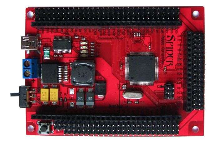
crack atmega1280p microprocessor fuse bit and readout embedded firmware from flash memory and eeprom memory
At the very start of period 2 in Figure 44 OCnx has a transition from high to low even though there is no Compare Match. The point of this transition is to guarantee symmetry around BOTTOM. There are two cases that give a transition without Compare Match. OCR0A changes its value from MAX, like in Figure 44. When the OCR0A value is MAX the OCn pin value is the same as the result of a down-counting Compare Match.
To ensure symmetry around BOTTOM the OCn value at MAX must correspond to the result of an up-counting Compare Match. The timer starts counting from a value higher than the one in OCR0A, and for that reason misses the Compare Match and hence the OCn change that would have happened on the way up. The Timer/Counter is a synchronous design and the timer clock (clkT0) is therefore shown as a clock enable signal in the following figures. The figures include information on when Interrupt Flags are set. Figure 45 contains timing data for basic Timer/Counter operation.
The figure shows the count sequence close to the MAX value in all modes other than phase correct PWM mode. These bits control the Output Compare pin (OC0B) behavior to recover atmega1280 mcu embedded heximal file. If one or both of the COM0B1:0 bits are set, the OC0B output overrides the normal port functionality of the I/O pin it is connected.
However, note that the Data Direction Register (DDR) bit corresponding to the OC0B pin must be set in order to enable the output driver. When OC0B is connected to the pin, the function of the COM0B1:0 bits depends on the WGM02:0 bit setting. Table 70 shows the COM0A1:0 bit functionality when the WGM02:0 bits are set to a normal or CTC mode (non-PWM).
Combined with the WGM02 bit found in the TCCR0B Register, these bits control the counting sequence of the counter, the source for maximum (TOP) counter value, and what type of waveform generation to be used. Modes of operation supported by the Timer/Counter unit are: Normal mode (counter), Clear Timer on Compare Match (CTC) mode, and two types of Pulse Width Modulation (PWM) modes.
Break MICROCONTROLLER ATMEGA640PA Flash
We can Break MICROCONTROLLER ATMEGA640PA Flash, please view the MICROCONTROLLER ATMEGA640PA features for your reference:
The phase correct PWM mode (WGM02:0 = 1 or 5) provides a high resolution phase correct PWM waveform generation option. The phase correct PWM mode is based on a dual-slope operation. The counter counts repeatedly from BOTTOM to TOP and then from TOP to BOTTOM when break microcontroller flash.
TOP is defined as 0xFF when WGM2:0 = 1, and OCR0A when WGM2:0 = 5. In non-inverting Compare Output mode, the Output Compare (OC0x) is cleared on the Compare Match between TCNT0 and OCR0x while upcounting, and set on the Compare Match while down-counting if break microcontroller flash.
In inverting Output Compare mode, the operation is inverted. The dual-slope operation has lower maximum operation frequency than single slope operation. However, due to the symmetric feature of the dual-slope PWM modes, these modes are preferred for motor control applications before break microcontroller flash.
In phase correct PWM mode the counter is incremented until the counter value matches TOP. When the counter reaches TOP, it changes the count direction. The TCNT0 value will be equal to TOP for one timer clock cycle after break microcontroller flash.
The timing diagram for the phase correct PWM mode is shown on Figure 44. The TCNT0 value is in the timing diagram shown as a histogram for illustrating the dual-slope operation. The diagram includes non-inverted and inverted PWM outputs if break microcontroller flash.
The small horizontal line marks on the TCNT0 slopes represent Compare Matches between OCR0x and TCNT0. The Timer/Counter Overflow Flag (TOV0) is set each time the counter reaches BOTTOM when break microcontroller flash.
The Interrupt Flag can be used to generate an interrupt each time the counter reaches the BOTTOM value. In phase correct PWM mode, the compare unit allows generation of PWM waveforms on the OC0x pins.
Setting the COM0x1:0 bits to two will produce a non-inverted PWM. An inverted PWM output can be generated by setting the COM0x1:0 to three: Setting the COM0A0 bits to one allows the OC0A pin to toggle on Compare Matches if the WGM02 bit is set. This option is not available for the OC0B pin after break microcontroller flash.
The actual OC0x value will only be visible on the port pin if the data direction for the port pin is set as output.
The PWM waveform is generated by clearing (or setting) the OC0x Register at the Compare Match between OCR0x and TCNT0 when the counter increments, and setting (or clearing) the OC0x Register at Compare Match between OCR0x and TCNT0 when the counter decrements. The PWM frequency for the output when using phase correct PWM can be calculated by the following equation when break microcontroller flash.
Reverse Engineering IC ATmega640A Heximal
Reverse Engineering IC ATmega640A to learn MCU ATmega640A circuitry pattern structure, the microcontroller ATmega640A will be unlocked and the heximal inside MCU ATmega640A flash memory can be readout:
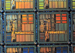
Reverse Engineering IC ATmega640A to learn MCU ATmega640A circuitry pattern structure, the microcontroller ATmega640A will be unlocked and the heximal inside MCU ATmega640A flash memory can be readout
The N variable represents the prescale factor (1, 8, 64, 256, or 1024). As for the Normal mode of operation, the TOV0 Flag is set in the same timer clock cycle that the counter counts from MAX to 0x00.
The fast Pulse Width Modulation or fast PWM mode (WGM02:0 = 3 or 7) provides a high frequency PWM waveform generation option. The fast PWM differs from the other PWM option by its single-slope operation. The counter counts from BOTTOM to TOP then restarts from BOTTOM. TOP is defined as 0xFF when WGM2:0 = 3, and OCR0A when WGM2:0 = 7.
In non-inverting Compare Output mode, the Output Compare (OC0x) is cleared on the Compare Match between TCNT0 and OCR0x, and set at BOTTOM. In inverting Compare Output mode, the output is set on Compare Match and cleared at BOTTOM before chip PIC16C62B eeprom content recovering.
Due to the single-slope operation, the operating frequency of the fast PWM mode can be twice as high as the phase correct PWM mode that use dual-slope operation.
This high frequency makes the fast PWM mode well suited for power regulation, rectification, and DAC applications. High frequency allows physically small sized external components (coils, capacitors), and therefore reduces total system cost.
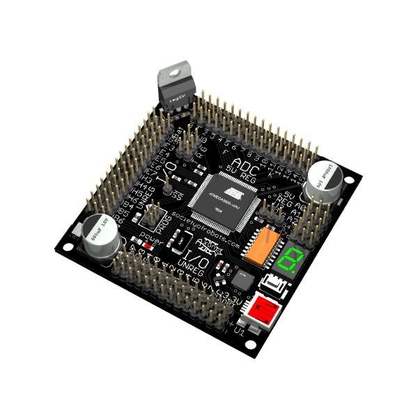
crack microcontroller ATMEGA640A fuse bit and readout source code from flash memory in the format of binary or heximal
In fast PWM mode, the counter is incremented until the counter value matches the TOP value. The counter is then cleared at the following timer clock cycle. The timing diagram for the fast PWM mode is shown in Figure 43. The TCNT0 value is in the timing diagram shown as a histogram for illustrating the single-slope operation when MCU PIC16C63A firmware recovery.
The diagram includes non-inverted and inverted PWM outputs. The small horizontal line marks on the TCNT0 slopes represent Compare Matches between OCR0x and TCNT0. The Timer/Counter Overflow Flag (TOV0) is set each time the counter reaches TOP. If the interrupt is enabled, the interrupt handler routine can be used for updating the compare value.
In fast PWM mode, the compare unit allows generation of PWM waveforms on the OC0x pins. Setting the COM0x1:0 bits to two will produce a non-inverted PWM and an inverted PWM output can be generated by setting the COM0x1:0 to three: Setting the COM0A1:0 bits to one allows the OC0A pin to toggle on Compare Matches if the WGM02 bit is set. This option is not available for the OC0B pin.
The actual OC0x value will only be visible on the port pin if the data direction for the port pin is set as output. The PWM waveform is generated by setting (or clearing) the OC0x Register at the Compare Match between OCR0x and TCNT0, and clearing (or setting) the OC0x Register at the timer clock cycle the counter is cleared (changes from TOP to BOTTOM).
Break Microcontroller ATmega640PV Binary
Break Microcontroller ATmega640PV program memory, and readout binary from MCU ATmega640PV, the firmware will include content from both eeprom and flash memory;
Break Microcontroller ATmega640PV program memory, and readout binary from MCU ATmega640PV, the firmware will include content from both eeprom and flash memory
In Clear Timer on Compare or CTC mode (WGM02:0 = 2), the OCR0A Register is used to manipulate the counter resolution.
In CTC mode the counter is cleared to zero when the counter value (TCNT0) matches the OCR0A. The OCR0A defines the top value for the counter, hence also its resolution.
This mode allows greater control of the Compare Match output frequency. It also simplifies the operation of counting external events.
The timing diagram for the CTC mode is shown in Figure 42. The counter value (TCNT0) increases until a Compare Match occurs between TCNT0 and OCR0A, and then counter (TCNT0) is cleared if reverse engineering microcontroller PIC16C620 code.
An interrupt can be generated each time the counter value reaches the TOP value by using the OCF0A Flag.
If the interrupt is enabled, the interrupt handler routine can be used for updating the TOP value. However, changing TOP to a value close to BOTTOM when the counter is running with none or a low prescaler value must be done with care since the CTC mode does not have the double buffering feature.
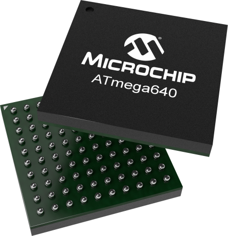
unlock avr mcu atmega640pv protection and copy embedded firmware from flash and eeprom memory
If the new value written to OCR0A is lower than the current value of TCNT0, the counter will miss the Compare Match.
The counter will then have to count to its maximum value (0xFF) and wrap around starting at 0x00 before the Compare Match can occur after microcontroller PIC16F620A binary recovery.
For generating a waveform output in CTC mode, the OC0A output can be set to toggle its logical level on each Compare Match by setting the Compare Output mode bits to toggle mode (COM0A1:0 = 1). The OC0A value will not be visible on the port pin unless the data direction for the pin is set to output.
The waveform generated will have a maximum frequency of fOC0 = fclk_I/O/2 when OCR0A is set to zero (0x00). The waveform frequency is defined by the following equation;
Break Microcontroller PIC24FJ16GA002 Heximal
Break Microcontroller PIC24FJ16GA002 program memory and data memory, readout heximal from MCU PIC24FJ16GA002 for microprocessor cloning.
Break Microcontroller PIC24FJ16GA002 program memory and data memory, readout heximal from MCU PIC24FJ16GA002 for microprocessor cloning
The mode of operation, i.e., the behavior of the Timer/Counter and the Output Compare pins, is defined by the combination of the Waveform Generation mode (WGM02:0) and Compare Output mode (COM0x1:0) bits.
The Compare Output mode bits do not affect the counting sequence, while the Waveform Generation mode bits do. The COM0x1:0 bits control whether the PWM output generated should be inverted or not (inverted or non-inverted PWM) if break microcontroller ATmega1284 memory.
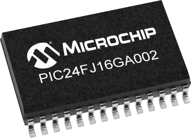
unlock PIC24FJ16GA002 microcontroller fuse bit and clone heximal program from flash memory
For non-PWM modes the COM0x1:0 bits control whether the output should be set, cleared, or toggled at a Compare Match (See “Compare Match Output Unit” on page 146.).For detailed timing information see “Timer/Counter Timing Diagrams”.
The simplest mode of operation is the Normal mode (WGM02:0 = 0). In this mode the counting direction is always up (incrementing), and no counter clear is performed. The counter simply overruns when it passes its maximum 8-bit value (TOP = 0xFF) and then restarts from the bottom (0x00) when microcontroller ATmega1284V memory reverse engineering.
In normal operation the Timer/Counter Overflow Flag (TOV0) will be set in the same timer clock cycle as the TCNT0 becomes zero. The TOV0 Flag in this case behaves like a ninth bit, except that it is only set, not cleared.
attack PIC24FJ16GA002 mcu protection and restore flash memory program and data file
However, combined with the timer overflow interrupt that automatically clears the TOV0 Flag, the timer resolution can be increased by software. There are no special cases to consider in the Normal mode, a new counter value can be written anytime. The Output Compare Unit can be used to generate interrupts at some given time.
Using the Output Compare to generate waveforms in Normal mode is not recommended, since this will occupy too much of the CPU time.
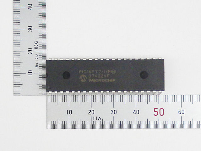
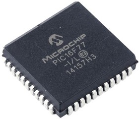
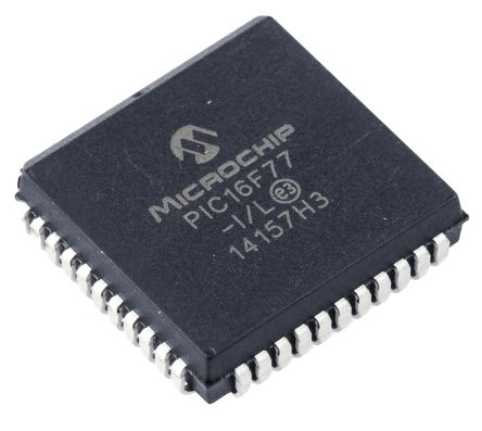
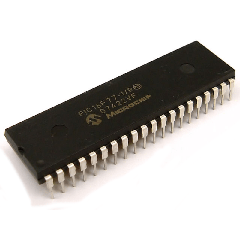
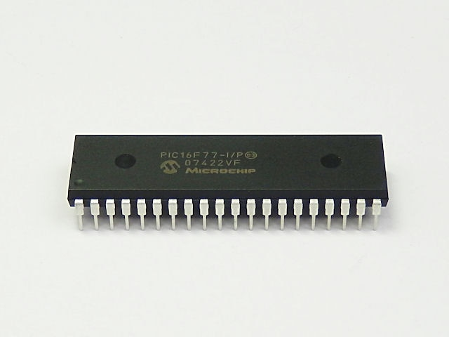
Recover MCU PIC16F77 Eeprom
The PIC16F77 microcontroller is a powerhouse of versatility within legacy industrial and commercial electronics, prized for its expansive input/output pin layout, dual capture/compare/PWM modules, and high-performance RISC architecture. This highly capable embedded controller serves as the central processing core in heavy-duty factory automation systems, HVAC control units, commercial vending machinery, and complex telecommunication routing hardware.
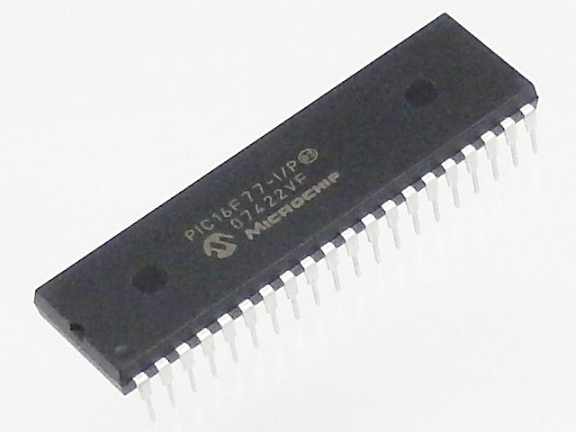
What sets this specific chip apart is its ability to handle dense, real-time operating parameters alongside a robust internal flash memory array and critical eeprom storage zones, which often hold unique calibration metrics, system runtime data, and cryptographic variables. Because these settings are fundamental to the host machine’s identity and function, manufacturers invariably engage the chip’s rigid, protective security fuses. Consequently, the chip operates in a permanently locked or encrypted environment, keeping the proprietary programming secured against direct read attempts or external tampering.
Program Memory Organization:
The PIC16F7X devices have a 13-bit program counter capable of addressing an 8K word x 14-bit program memory space. The PIC16F77/76 devices have 8K words of FLASH program memory and the PIC16F73/74 devices have 4K words. The program memory maps for PIC16F7X devices are shown in Figure 2-1. Accessing a location above the physically implemented address will cause a wraparound. in the PICmicro Mid-Range Reference Manual.
The 28-pin devices have 11 interrupts, while the 40/44-pin devices have 12
· The 28-pin devices have 5 A/D input channels, while the 40/44-pin devices have 8
· The Parallel Slave Port is implemented only on the 40/44-pin devices
The RESET Vector is at 0000h and the Interrupt Vector is at 0004h;
Each bank extends up to 7Fh (128 bytes). The lower locations of each bank are reserved for the Special Function Registers. Above the Special Function Registers are General Purpose Registers, implemented as
static RAM. All implemented banks contain Special
Function Registers. Some frequently used Special
Function Registers from one bank may be mirrored in
another bank for code reduction and quicker access. implemented address will cause a wraparound. in the PICmicro Mid-Range Reference Manual
The 28-pin devices have 11 interrupts, while the 40/44-pin devices have 12
· The 28-pin devices have 5 A/D input channels, while the 40/44-pin devices have 8
· The Parallel Slave Port is implemented only on the 40/44-pin devices.
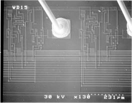
When an industrial facility or hardware engineering team encounters a critical system failure paired with a complete loss of the original source code or project archive, our dedicated laboratory provides a vital lifeline to recover MCU PIC16F77 eeprom allocations and firmware. Overcoming the integrated security flags of an obsolete microcontroller requires a sophisticated blend of material science and micro-electronics engineering. Our specialists approach this task by utilizing a highly precise physical methodology: we carefully decapsulate the resilient plastic package using controlled chemical or mechanical etching to bring the microscopic silicon die into view. Once the internal micro-structures are accessible, engineers can decode the physical state of the memory cells and attack the embedded security lock bits. By understanding the chip’s internal layout, we can safely break past the hardware-level restrictions, allowing us to hack the read-protection barriers, retrieve the uncorrupted binary data, and extract the complete heximal file flawlessly.
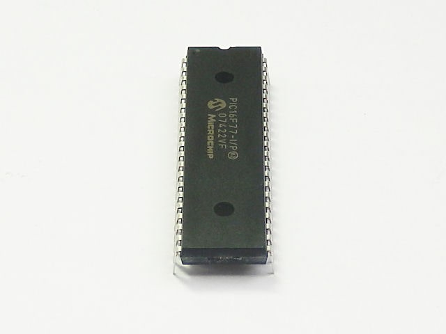
The core purpose of this micro-engineering intervention is to safeguard industrial longevity and eliminate the astronomical costs associated with unplanned system redesigns. When a vital piece of production equipment goes offline due to a corrupted or inaccessible chip, trying to rewrite the original program from scratch can take months of speculative engineering. Our technical services allow clients to seamlessly duplicate or clone the exact operational parameters of the failing device onto replacement hardware. The major benefit for the end user is a fast, non-destructive, and predictable restoration pathway that breathes new life into obsolete infrastructure. By transforming an unreadable, protected microcontroller into a fully accessible data asset, we ensure your daily business operations continue smoothly, entirely insulated from the threat of hardware obsolescence.
Reverse Engineering MCU ATMEGA640P Flash
Reverse Engineering MCU ATmega640P to figure out the location of security fuse bit of Microcontroller ATmega640P by MCU cracking technique, then extract code from microcontroller ATmega640P Flash memory;
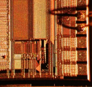
Reverse Engineering MCU ATMEGA640P to figure out the location of security fuse bit of Microcontroller ATmega640P by MCU cracking technique, then extract code
The Compare Output mode (COM0x1:0) bits have two functions. The Waveform Generator uses the COM0x1:0 bits for defining the Output Compare (OC0x) state at the next Compare Match. Also, the COM0x1:0 bits control the OC0x pin output source. Figure 41 shows a simplified schematic of the logic affected by the COM0x1:0 bit setting if MCU ATmega644 code recovering.
The I/O Registers, I/O bits, and I/O pins in the figure are shown in bold. Only the parts of the general I/O Port Control Registers (DDR and PORT) that are affected by the COM0x1:0 bits are shown. When referring to the OC0x state, the reference is for the internal OC0x Register, not the OC0x pin. If a system reset occur, the OC0x Register is reset to “0”.
The general I/O port function is overridden by the Output Compare (OC0x) from the Waveform Generator if either of the COM0x1:0 bits are set. However, the OC0x pin direction (input or output) is still controlled by the Data Direction Register (DDR) for the port pin. The Data Direction Register bit for the OC0x pin (DDR_OC0x) must be set as output before the OC0x value is visible on the pin. The port override function is independent of the Waveform Generation mode.
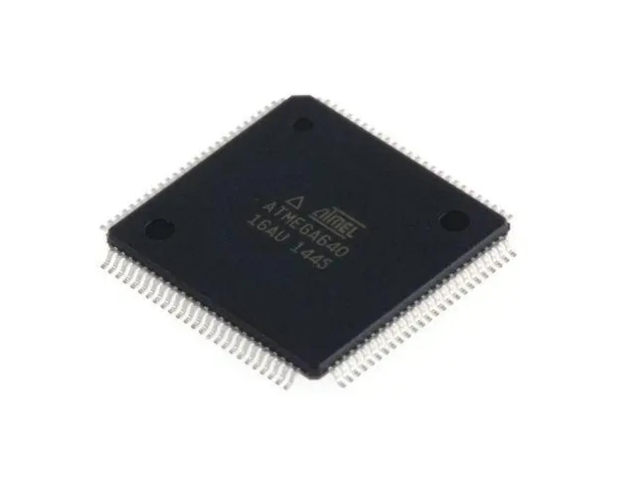
unlock ATMEGA640A atmel microprocessor secured and recover embedded heximal data from flash memory
The design of the Output Compare pin logic allows initialization of the OC0x state before the output is enabled. Note that some COM0x1:0 bit settings are reserved for certain modes of operation. See “8-bit Timer/Counter Register Description”.
The Waveform Generator uses the COM0x1:0 bits differently in Normal, CTC, and PWM modes. For all modes, setting the COM0x1:0 = 0 tells the Waveform Generator that no action on the OC0x Register is to be performed on the next Compare Match.
For compare output actions in the non-PWM modes refer to Table 70 on page 128. For fast PWM mode, refer to Table 71 on page 128, and for phase correct PWM refer to Table 72 on page 129. A change of the COM0x1:0 bits state will have effect at the first Compare Match after the bits are written. For non-PWM modes, the action can be forced to have immediate effect by using the FOC0x strobe bits.
Recover MCU PIC16F73 Binary
Recover MCU PIC16F73 Binary from flash memory and data extracted from eeprom memory of Microcontroller, reprogramme the firmware into blank MCU PIC16F73 for Microprocessor cloning;
Recover MCU PIC16F73 Binary from flash memory and data extracted from eeprom memory of Microcontroller, reprogramme the firmware into blank MCU PIC16F73 for Microprocessor cloning
High Performance RISC CPU:
· High performance RISC CPU
· Only 35 single word instructions to learn
· All single cycle instructions except for program branches which are two-cycle
· Operating speed: DC – 20 MHz clock input DC – 200 ns instruction cycle
· Up to 8K x 14 words of FLASH Program Memory, Up to 368 x 8 bytes of Data Memory (RAM)
· Pinout compatible to the PIC16C73B/74B/76/77
· Pinout compatible to the PIC16F873/874/876/877
· Interrupt capability (up to 12 sources)
· Eight level deep hardware stack
· Direct, Indirect and Relative Addressing modes
· Processor read access to program memory
Special Microcontroller Features:
· Power-on Reset (POR)
· Power-up Timer (PWRT) and
Oscillator Start-up Timer (OST)
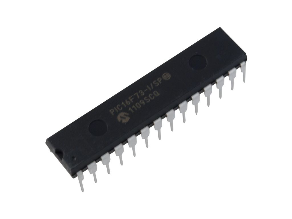
unlock PIC16F73 microprocessor fuse bit and open mcu flash memory and eeprom memory to readout heximal program and binary data
· Watchdog Timer (WDT) with its own on-chip RC oscillator for reliable operation
· Programmable code protection
· Power saving SLEEP mode
· Selectable oscillator options
· In-Circuit Serial Programming (ICSP) via two pins
Peripheral Features:
· Timer0: 8-bit timer/counter with 8-bit prescaler
· Timer1: 16-bit timer/counter with prescaler, can be incremented during SLEEP via external crystal/clock
· Timer2: 8-bit timer/counter with 8-bit period register, prescaler and postscaler
· Two Capture, Compare, PWM modules if Recover mcu binary
– Capture is 16-bit, max. resolution is 12.5 ns
– Compare is 16-bit, max. resolution is 200 ns
– PWM max. resolution is 10-bit
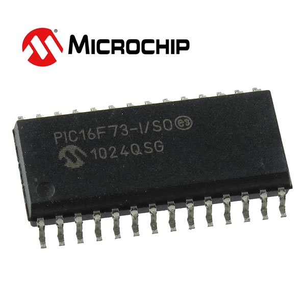
recover pic16F73 mcu chip flash memory code and clone the program firmware to new microcontroller
· 8-bit, up to 8-channel Analog-to-Digital converter
· Synchronous Serial Port (SSP) with SPI (Master mode) and I2C (Slave)
· Universal Synchronous Asynchronous Receiver Transmitter (USART/SCI)
· Parallel Slave Port (PSP), 8-bits wide with external RD, WR and CS controls (40/44-pin only)
· Brown-out detection circuitry for Brown-out Reset (BOR)
Recover Chip ATmega640P Heximal
Recover Chip ATmega640P Heximal from Microcontroller ATmega640P flash and eeprom memory, rewrite the firmware to blank MCU ATmega640P by Microprocessor copying technique, unlock MCU secured system and reset the status of Microcontroller from locked to unlocked;
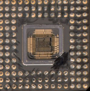
Recover Chip ATmega640P Heximal from Microcontroller ATmega640P flash and eeprom memory, rewrite the firmware to blank MCU ATmega640P by Microprocessor copying technique, unlock MCU secured system and reset the status of Microcontroller from locked to unlocked
In non-PWM waveform generation modes, the match output of the comparator can be forced by writing a one to the Force Output Compare (FOC0x) bit. Forcing Compare Match will not set the OCF0x Flag or reload/clear the timer, but the OC0x pin will be updated as if a real Compare Match had occurred (the COM0x1:0 bits settings define whether the OC0x pin is set, cleared or toggled) if MCU PIC16F917 heximal breaking.
All CPU write operations to the TCNT0 Register will block any Compare Match that occur in the next timer clock cycle, even when the timer is stopped. This feature allows OCR0x to be initialized to the same value as TCNT0 without triggering an interrupt when the Timer/Counter clock is enabled.
Since writing TCNT0 in any mode of operation will block all Compare Matches for one timer clock cycle, there are risks involved when changing TCNT0 when using the Output Compare Unit, independently of whether the Timer/Counter is running or not after recover MCU PIC16F72 code.
If the value written to TCNT0 equals the OCR0x value, the Compare Match will be missed, resulting in incorrect waveform generation. Similarly, do not write the TCNT0 value equal to BOTTOM when the counter is down-counting.
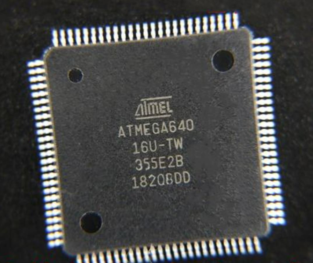
microprocessor atmega640v protection unlocking and readout embedded firmware
The setup of the OC0x should be performed before setting the Data Direction Register for the port pin to output. The easiest way of setting the OC0x value is to use the Force Output Compare (FOC0x) strobe bits in Normal mode if recover MCU PIC16F77 eeprom heximal.
The OC0x Registers keep their values even when changing between Waveform Generation modes. Be aware that the COM0x1:0 bits are not double buffered together with the compare value. Changing the COM0x1:0 bits will take effect immediately.