Archive for the ‘Reverse Engineer Microcontroller’ Category
 Copy Microcontroller PIC18F4220 Binary
 August 20th, 2014 |
  Author:
 Memory Endurance: The Enhanced Flash cells for both program memory and data EEPROM are rated to last for many thousands of erase/write cycles – up to 100,000 for program memory and 1,000,000 for EEPROM which has provide a preferential terms for Copy Microcontroller PIC18F4220 Binary. Data retention without refresh is conservatively estimated to be greater than 40 years.
· Self-programmability: These devices can write to their own program memory spaces under internal software control. By using a bootloader routine located in the protected Boot Block at the top of program memory, it becomes possible to create an application that can update itself in the field.
· Enhanced CCP Module: In PWM mode, this module provides 1, 2 or 4 modulated outputs for controlling half-bridge and full-bridge drivers. Other features include Auto-Shutdown for disabling PWM outputs on interrupt or other select conditions and Auto-Restart to reactivate outputs once the condition has cleared.
Addressable USART: This serial communication module is capable of standard RS-232 operation using the internal oscillator block, removing the need for an external crystal (and its accompanying power requirement) in applications that talk to the outside world.
· 10-bit A/D Converter: This module incorporates programmable acquisition time, allowing for a channel to be selected and a conversion to be initiated without waiting for a sampling period and thus, reduce code overhead.
· Extended Watchdog Timer (WDT): This enhanced version incorporates a 16-bit prescaler, allowing a time-out range from 4 ms to over 2 minutes, that is stable across operating voltage and temperature.
The EC and ECIO Oscillator modes require an external clock source to be connected to the OSC1 pin. There is no oscillator start-up time required after a Power-on Reset or after an exit from Sleep mode after Copy Microcontroller PIC18F4220 Binary.
In the EC Oscillator mode, the oscillator frequency divided by 4 is available on the OSC2 pin. This signal may be used for test purposes or to synchronize other logic. Figure 2-4 shows the pin connections for the EC Oscillator mode.
For timing insensitive applications, the “RC” and “RCIO” device options offer additional cost savings. The RC oscillator frequency is a function of the supply voltage, the resistor (REXT) and capacitor (CEXT) values and the operating temperature.
In addition to this, the oscillator frequency will vary from unit to unit due to normal manufacturing variation. Furthermore, the difference in lead frame capacitance between package types will also affect the oscillation frequency, especially for low CEXT values.
The user also needs to take into account variation due to tolerance of external R and C components used. Figure 2-6 shows how the R/C combination is connected. In the RC Oscillator mode, the oscillator frequency divided by 4 is available on the OSC2 pin. This signal may be used for test purposes or to synchronize other logic.
Copy MCU PIC16C72 Software
We can Copy MCU PIC16C72 Software, please see the MCU PIC16C72 features for your reference:
PIC16C7X Microcontroller Core Features:
· High-performance RISC CPU
· Only 35 single word instructions to learn
· All single cycle instructions except for program branches which are two cycle
· Operating speed: DC – 20 MHz clock input DC – 200 ns instruction cycle
· Up to 8K x 14 words of Program Memory, up to 368 x 8 bytes of Data Memory (RAM)
· Interrupt capability
· Eight level deep hardware stack
· Direct, indirect, and relative addressing modes
· Power-on Reset (POR)
Copy MCU PIC16C72 Software
· Power-up Timer (PWRT) and Oscillator Start-up Timer (OST)
· Watchdog Timer (WDT) with its own on-chip RC oscillator for reliable operation
· Programmable code-protection
· Power saving SLEEP mode
· Selectable oscillator options
· Low-power, high-speed CMOS EPROM technology
· Fully static design
· Wide operating voltage range: 2.5V to 6.0V
· High Sink/Source Current 25/25 mA
· Commercial, Industrial and Extended temperature ranges
· Low-power consumption:
· < 2 mA @ 5V, 4 MHz
· 15 µA typical @ 3V, 32 kHz
· < 1 µA typical standby current
PIC16C7X Peripheral Features:
· Timer0: 8-bit timer/counter with 8-bit prescaler
· Timer1: 16-bit timer/counter with prescaler, can be incremented during sleep via external crystal/clock
· Timer2: 8-bit timer/counter with 8-bit period register, prescaler and postscaler
· Capture, Compare, PWM module(s)
· Capture is 16-bit, max. resolution is 12.5 ns, Compare is 16-bit, max. resolution is 200 ns, PWM max. resolution is 10-bit from Copy MCU PIC16C72 Software
· 8-bit multichannel analog-to-digital converter
· Synchronous Serial Port (SSP) with SPI and I2C
· Universal Synchronous Asynchronous Receiver Transmitter (USART/SCI)
· Parallel Slave Port (PSP) 8-bits wide, with external RD, WR and CS controls
· Brown-out detection circuitry for Brown-out Reset (BOR)
Copy CPLD XC2C128_VQ100 Content
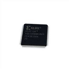
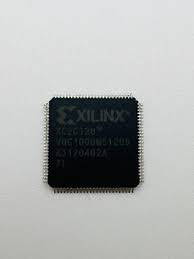
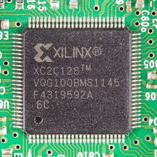
The XC2C128_VQ100 is a high-performance PLD widely integrated into modern embedded systems requiring deterministic logic control and flexible configuration. With its non-volatile architecture and efficient power profile, this device is frequently used in telecommunications infrastructure, industrial controllers, automotive electronics, and aerospace subsystems. It manages complex logic operations while securely storing critical firmware, program structures, and configuration data within internal memory. In many deployments, this information is intentionally protected, locked, or encrypted, preventing unauthorized duplication of valuable source code, binary, or heximal files that define the device’s functionality.
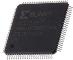
Our “Copy CPLD XC2C128_VQ100 Content” service is engineered to attack, break, and decode even the most secured and protective configurations embedded within the chip. By applying advanced decapsulate techniques alongside non-invasive electrical analysis, we can retrieve critical firmware, extract structured binary and heximal data, and reconstruct usable source code from the internal memory space. Whether the design is stored in flash, EEPROM, or proprietary configuration cells, our process enables us to effectively hack through encrypted and locked barriers. The recovered archive is then processed into a complete program file, allowing clients to clone, duplicate, or redeploy the original logic design across new hardware platforms with precision and consistency.
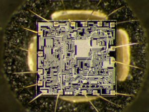
We can Copy CPLD XC2C128_VQ100 Content, please view below CPLD XC2C128_VQ100 features for your reference:
Features
· Optimized for 1.8V systems
– Industry’s fastest low power CPLD
– Densities from 32 to 512 macrocells
· Industry’s best 0.18 micron CMOS CPLD
– Optimized architecture for effective logic synthesis by Copy CPLD XC2C128_VQ100 Content
– Multi-voltage I/O operation — 1.5V to 3.3V
· Advanced system features
– Fastest in system programming
· 1.8V ISP using IEEE 1532 (JTAG) interface
– On-The-Fly Reconfiguration (OTF)
– IEEE1149.1 JTAG Boundary Scan Test
– Optional Schmitt trigger input (per pin)
– Multiple I/O banks on all devices
– Unsurpassed low power management
– SSTL2_1,SSTL3_1, and HSTL_1 on 128 macrocell and denser devices
– Hot pluggable PLA architecture
– Superior pinout retention
– 100% product term routability across function block Wide package availability including fine pitch:
– Chip Scale Package (CSP) BGA, Fine Line BGA, TQFP, PQFP, VQFP, and QFN packages
Free software support for all densities using Xilinx® WebPACK™ tool Industry leading nonvolatile 0.18 micron CMOS
· DataGATE external signal control
– Flexible clocking modes
· Optional DualEDGE triggered registers
· Clock divider (÷ 2,4,6,8,10,12,14,16)
· CoolCLOCK
– Global signal options with macrocell control
· Multiple global clocks with phase selection per macrocell
· Multiple global output enables
· Global set/reset
– Abundant product term clocks, output enables and set/resets
– Efficient control term clocks, output enables and set/resets for each macrocell and shared across function blocks from Copy CPLD XC2C128_VQ100 Content
– Advanced design security
– Open-drain output option for Wired-OR and LED drive
– Optional bus-hold, 3-state or weak pullup on select I/O pins
– Optional configurable grounds on unused I/Os
– Mixed I/O voltages compatible with 1.5V, 1.8V, process
– Guaranteed 1,000 program/erase cycles
– Guaranteed 20 year data retention
Family Overview
Xilinx CoolRunner™-II CPLDs deliver the high speed and ease of use associated with the XC9500/XL/XV CPLD family with the extremely low power versatility of the XPLA3 family in a single MCU Recovery. This means that the exact same parts can be used for high-speed data communications.
computing systems and leading edge portable products, with the added benefit of In System Programming. Low power consumption and high-speed operation are combined into a single family that is easy to use and cost effective. Clocking techniques and other power saving features extend the users’ power budget. The design features are supported starting with Xilinx ISE® 4.1i WebPACK tool.
From a technical perspective, the methodology combines both physical inspection and algorithmic reconstruction. During the decapsulation stage, the silicon structure is exposed to allow direct interaction with internal nodes, enabling deeper retrieval of embedded data. Parallel to this, logical decode procedures interpret raw binary dumps into structured firmware formats, ensuring that each file within the archive is accurate and functional. This dual approach significantly improves the success rate when dealing with highly protected or encrypted CPLD devices. As a result, clients receive not just raw data, but a refined and usable representation of the original program and source code, ready for analysis, modification, or reproduction.
The ability to copy, clone, and restore CPLD content has become essential in industries facing component discontinuation, lack of design documentation, or the need for system replication. By leveraging our expertise to attack, decode, and extract secured memory, customers gain full access to otherwise inaccessible firmware and data assets. This enables efficient maintenance, redesign, and long-term support of critical systems without dependence on original suppliers. Ultimately, our service provides a reliable and technically robust pathway to unlock, understand, and duplicate the functional core of the XC2C128_VQ100, delivering measurable value in both engineering flexibility and operational continuity.
Copy Chip PIC16F74A Binary
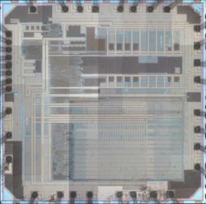
Copy Chip PIC16F74A Binary
The high performance of the PIC16CXX family can be attributed to a number of architectural features commonly found in RISC microprocessors. To begin with, the PIC16CXX uses a Harvard architecture, in which, program and data are accessed from separate memories using separate buses to Copy Chip PIC16F74A Binary. This improves bandwidth over traditional von Neumann architecture in which program and data are fetched from the same memory using the same bus.
Separating program and data buses further allows instructions to be sized differently than the 8-bit wide data word. Instruction opcodes are 14-bits wide making it possible to have all single word instructions by Recovery MICROCONTROLLER ATMEGA48A Program. A 14-bit wide program memory access bus fetches a 14-bit instruction in a single cycle.
A two-stage pipeline overlaps fetch and execution of instructions. Consequently, all instructions (35) execute in a single cycle (200 ns @ 20 MHz) except for program branches.
The PIC16CXX can directly or indirectly address its register files or data memory. All special function registers, including the program counter, are mapped in the data memory. The PIC16CXX has an orthogonal (symmetrical) instruction set that makes it possible to carry out any operation on any register using any addressing mode.
This symmetrical nature and lack of ‘special optimal situations’ make programming with the PIC16CXX simple yet efficient. In addition, the learning curve is reduced significantly.
PIC16CXX devices contain an 8-bit ALU and working register. The ALU is a general purpose arithmetic unit to Break MCU ATMEGA168A Flash, It performs arithmetic and Boolean functions between the data in the working register and any register file.
The ALU is 8-bits wide and capable of addition, subtraction, shift and logical operations. Unless otherwise mentioned, arithmetic operations are two’s complement in nature. In two-operand instructions, typically one operand is the working register (W register) from Copy Chip PIC16F74A Binary. The other operand is a file register or an immediate constant.
In single operand instructions, the operand is either the W register or a file register. The W register is an 8-bit working register used for ALU operations. It is not an addressable register. Depending on the instruction executed, the ALU may affect the values of the Carry (C), Digit Carry (DC), and Zero (Z) bits in the STATUS register to Recover IC ATMEGA168PA Program. The C and DC bits operate as a borrow bit and a digit borrow out bit, respectively, in subtraction. See theSUBLW and SUBWF instructions for examples after clone IC.
 Posted in Reverse Engineer Microcontroller |
  Tags: атакувати ic archive, атакувати mcu code, атакувати інтегральна схема file, атакувати мікроконтролер data, атакувати чіп software, зломити ic bin, зломити mcu hex, зломити інтегральна схема flash, зломити мікроконтролер eeprom, зломити чіп firmware |
  Comments Closed
Copy Microcontroller PIC16C770 Eeprom
The PIC16C770 microcontroller has long been used in embedded control systems where compact design, stable performance, and cost efficiency are essential. It can be found in industrial controllers, sensor modules, measurement equipment, power management units, and various consumer electronic devices. With its integrated EEPROM, reliable program memory architecture, and flexible peripheral configuration, the PIC16C770 is well suited for systems that must store calibration parameters, configuration data, and embedded firmware logic. However, in many legacy devices the original firmware archive, binary file, or source code documentation is no longer available, making maintenance or system duplication extremely difficult. In these situations, a specialized Copy Microcontroller PIC16C770 Eeprom service becomes a valuable solution for recovering critical embedded data and preserving long-term system functionality.
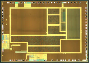
In practical embedded products, manufacturers frequently enable protective, protected, locked, or encrypted configurations to secure firmware and program memory stored inside the microcontroller. These mechanisms protect intellectual property but can also prevent legitimate recovery when systems must be repaired or upgraded. Our Copy Microcontroller PIC16C770 Eeprom service focuses on helping authorized clients attack, break, or carefully decode these restrictions in a controlled engineering environment in order to retrieve valuable firmware, binary, or heximal data from flash and EEPROM memory. Through advanced analysis, our engineers can reconstruct program file archives and restore embedded data structures when the original development materials have been lost. In complex scenarios where internal protection mechanisms prevent normal access, specialized techniques including controlled decapsulate procedures may be considered to reach secured memory regions and extract the required firmware content.
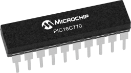
This document contains device-specific information. Additional information may be found in the PICmicroTM Mid-Range Reference Manual, (DS33023), which may be obtained from your local Micromicrocontroller Sales Representative or downloaded from the Micromicrocontroller website.
The Reference Manual should be considered a complementary document to this data sheet, and is highly recommended copying for a better understanding of the device architecture and operation of the peripheral modules.
There are two memory blocks in each of these PICmicro ® microcontrollers. Each block (Program Memory and Data Memory) has its own bus, so that concurrent access can occur. Additional information on device memory may be found in the PICmicro Mid-Range Reference Manual, (DS33023).
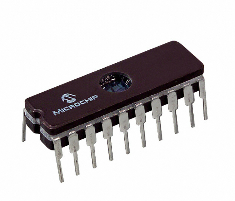
The PIC16C717/770/771 devices have a 13-bit program counter capable of addressing an 8K x 14 program memory space. The PIC16C717 and the PIC16C770 have 2K x 14 words of program memory. The PIC16C771 has 4K x 14 words of program memory. Accessing a location above the physically implemented address will cause a wraparound which can facilitate the MCU Cracking.
The reset vector is at 0000h and the interrupt vector is at 0004h. Each bank extends up to 7Fh (128 bytes). The lower locations of each bank are reserved for the Special Function Registers. Above the Special Function Registers are General Purpose Registers, implemented as static RAM. All implemented banks contain special function registers if Copy Microcontroller. Some frequently used special function registers from one bank are mirrored in another bank for code reduction and quicker access.
The Special Function Registers are registers used by the CPU and Peripheral Modules for controlling the desired operation of the device. These registers are implemented as static RAM. The special function registers can be classified into two sets; core (CPU) and peripheral. Those registers associated with the core functions are described in detail in this section. Those related to the operation of the peripheral features are described in detail in that peripheral feature section.
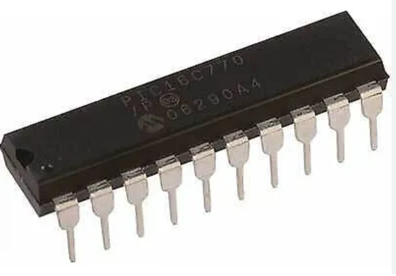
Once the embedded memory data has been successfully retrieved, the next stage is to convert raw dumps into structured and usable program assets. Firmware blocks stored in flash and configuration parameters stored in EEPROM are carefully analyzed, verified, and organized into reliable binary or heximal program files. These reconstructed archives allow clients to clone or duplicate the original microcontroller functionality on replacement devices while maintaining compatibility with existing hardware systems. By decoding secured firmware structures and rebuilding program data, our service enables companies to preserve embedded logic that would otherwise be inaccessible due to lost source code or protected device configurations.
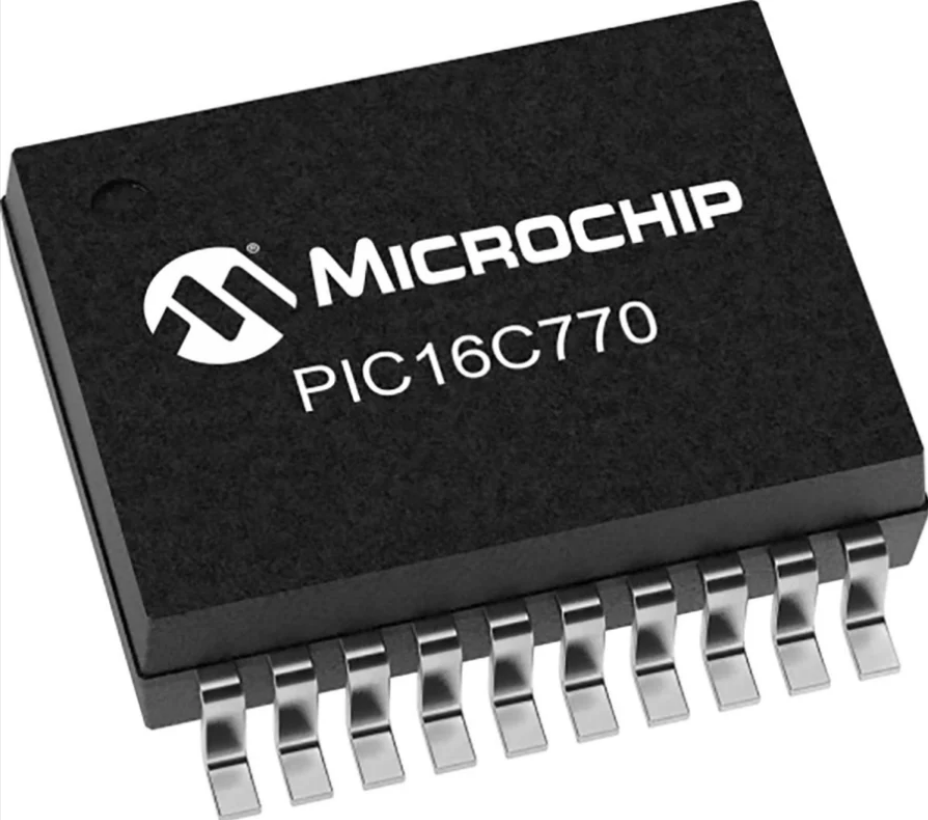
The advantages for end users are significant. Recovering the firmware and EEPROM data from a PIC16C770 microcontroller allows companies to maintain legacy equipment, support spare unit production, and avoid expensive system redesign. Industrial operators, equipment manufacturers, and maintenance providers can extend the lifecycle of deployed devices while ensuring operational stability. Instead of abandoning proven hardware due to locked or secured microcontrollers, organizations can regain access to their embedded program logic and memory resources. Through careful handling of protected devices and disciplined firmware reconstruction methods, our Copy Microcontroller PIC16C770 Eeprom service provides a reliable path for retrieving valuable embedded data and sustaining critical electronic systems across many industries.
Copy AVR ATmega161 Firmware
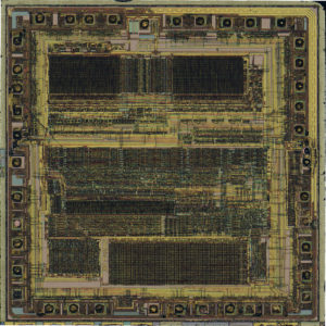
Copy AVR ATmega161 Firmware
We can Copy AVR ATMEGA161 Firmware, please view below the feature of AVR ATMEGA161 for our reference:
Features
· High-performance, Low-power AVR® 8-bit Microcontroller
· Advanced RISC Architecture
– 130 Powerful Instructions – Most Single Clock Cycle Execution
– 32 x 8 General Purpose Working Registers
– Fully Static Operation
– Up to 8 MIPS Throughput at 8 MHz
– On-chip 2-cycle Multiplier
Program and Data Memories
– 16K Bytes of Non-volatile In-System Programmable Flash Endurance: 1,000 Write/Erase Cycles
– Optional Boot Code Memory with Independent Lock bits Self-programming of Program and Data Memories
– 512 Bytes of Non-volatile In-System Programmable EEPROM Endurance: 100,000 Write/Erase Cycles
– 1K Byte of Internal SRAM
– Programming Lock for Software Security
Peripheral Features
– Two 8-bit Timer/Counters with Separate Prescaler and PWM
– Expanded 16-bit Timer/Counter System with Separate Prescaler, Compare, Capture Modes and Dual 8-, 9-, or 10-bit PWM after Copy AVR
– Dual Programmable Serial UARTs
– Master/Slave SPI Serial Interface
– Real-time Counter with Separate Oscillator
– Programmable Watchdog Timer with Separate On-chip Oscillator
– On-chip Analog Comparator
Special Microcontroller Features
– External and Internal Interrupt Sources
– Three Sleep Modes: Idle, Power-save and Power-down Power Comsumption at 4 MHz, 3.0V, 25°C
– Active 3.0 mA
– Idle Mode 1.2 mA
– Power-down Mode < 1 µA
I/O and Packages
– 35 Programmable I/O Lines
– 40-lead PDIP and 44-lead TQFP Operating Voltages
– 2.7V – 5.5V for the ATmega161L
– 4.0V – 5.5V for the ATmega161 Speed Grades
– 0 – 4 MHz for the ATmega161L
– 0 – 8 MHz for the ATmega161
Commercial and Industrial Temperature Ranges
Posted in Reverse Engineer Microcontroller |
Tags: copy avr encrypted archive, copy avr encrypted code, copy avr encrypted dump, copy avr encrypted eeprom, copy avr encrypted firmware, copy avr encrypted information, copy avr encrypted memory, copy avr encrypted program, vervielfältigen mcu bin, vervielfältigen mcu code, vervielfältigen mcu data, vervielfältigen mcu eeprom, vervielfältigen mcu file, vervielfältigen mcu firmware, vervielfältigen mcu flash, vervielfältigen mcu hex, vervielfältigen mcu memory |
Comments Closed
Copy AVR ATmega165A
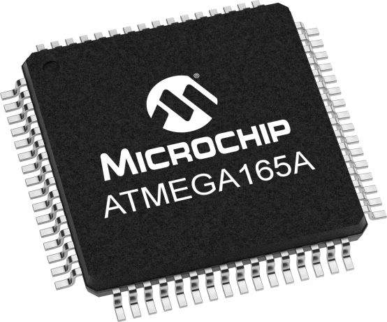
Copy AVR ATmega165A is a specialized firmware recovery and duplication service created for organizations that rely on long-life embedded systems and require continued access to critical program assets. The ATmega165A is a versatile 8-bit AVR microcontroller widely used in industrial automation, smart metering, HVAC controllers, laboratory instruments, consumer electronics, and embedded communication modules. With its integrated flash memory, EEPROM, SRAM, and rich peripheral set, it offers stable performance and low-power operation for applications that demand reliability over extended product lifecycles. When original development teams move on or documentation is lost, maintaining continuity of firmware and program files becomes a strategic necessity.
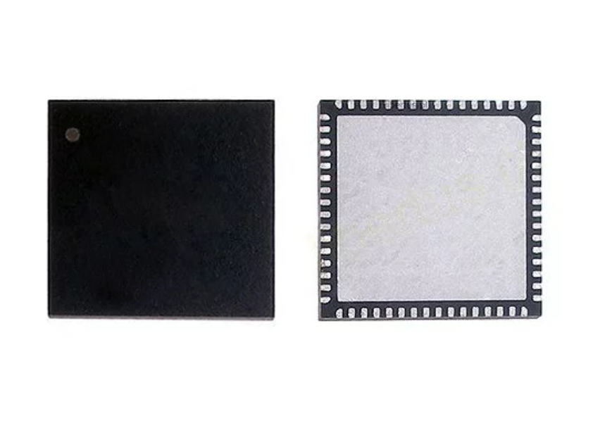
In many deployed systems, the ATmega165A is configured with protective, protected, locked, or encrypted security settings to secure firmware, binary, or heximal content stored in flash and EEPROM memory. Our Copy AVR ATmega165A service focuses on helping authorized clients attack and break these access controls in a controlled and compliant engineering environment. Through advanced analysis, we work to decode secured memory regions, retrieve embedded firmware data, and reconstruct usable program archives when source code or archived files are unavailable. In complex cases, controlled decapsulation concepts may be applied to access deeply embedded memory structures. The objective is not merely to hack a device, but to retrieve, clone, or duplicate consistent firmware, binary, and heximal outputs that can be validated and prepared for production continuity.
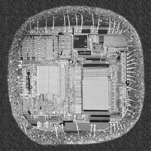
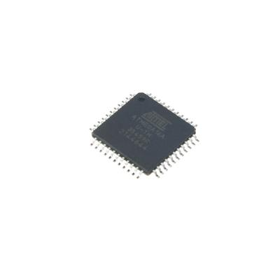
We can Copy AVR ATmega165A, please view below the feature of AVR ATmega165A for your reference:
Features
High Performance, Low Power Atmel® AVR® 8-Bit Microcontroller
Advanced RISC Architecture
– 130 Powerful Instructions – Most Single Clock Cycle Execution
– 32 x 8 General Purpose Working Registers
– Fully Static Operation
– Up to 16MIPS Throughput at 16MHz (ATmega165PA/645P)
– Up to 20MIPS Throughput at 20MHz
(ATmega165A/325A/325PA/645A/3250A/3250PA/6450A/6450P)
– On-Chip 2-cycle Multiplier
High Endurance Non-volatile Memory segments
– In-System Self-programmable Flash Program Memory
· 16KBytes (ATmega165A/ATmega165PA)
· 32KBytes (ATmega325A/ATmega325PA/ATmega3250A/ATmega3250PA)
· 64KBytes (ATmega645A/ATmega645P/ATmega6450A/ATmega6450P)
– EEPROM
· 512Bytes (ATmega165A/ATmega165PA)
· 1Kbytes (ATmega325A/ATmega325PA/ATmega3250A/ATmega3250PA)
· 2Kbytes (ATmega645A/ATmega645P/ATmega6450A/ATmega6450P)
– Internal SRAM
· 1KBytes (ATmega165A/ATmega165PA)
· 2KBytes (ATmega325A/ATmega325PA/ATmega3250A/ATmega3250PA)
· 4KBytes (ATmega645A/ATmega645P/ATmega6450A/ATmega6450P)
– Write/Erase cycles: 10,000 Flash/100,000 EEPROM
– Data retention: 20 years at 85°C/100 years at 25°C(1)
– Optional Boot Code Section with Independent Lock Bits
· In-System Programming by On-chip Boot Program
· True Read-While-Write Operation
– Programming Lock for Software Security
– Capacitive touch buttons, sliders and wheels
– Up to 64 sense channels
JTAG (IEEE std. 1149.1 compliant) Interface
– Boundary-scan Capabilities According to the JTAG Standard
– Extensive On-chip Debug Support
– Programming of Flash, EEPROM, Fuses, and Lock Bits through the JTAG Interface
Peripheral Features
– Two 8-bit Timer/Counters with Separate Prescaler and Compare Mode
– One 16-bit Timer/Counter with Separate Prescaler, Compare Mode, and Capture Mode
– Real Time Counter with Separate Oscillator
– Four PWM Channels
– 8-channel, 10-bit ADC
– Programmable Serial USART
– Master/Slave SPI Serial Interface
– Universal Serial Interface with Start Condition Detector
– Programmable Watchdog Timer with Separate On-chip Oscillator
– On-chip Analog Comparator
– Interrupt and Wake-up on Pin Change
Special Microcontroller Features
– Power-on Reset and Programmable Brown-out Detection
– Internal Calibrated Oscillator
– External and Internal Interrupt Sources
– Five Sleep Modes: Idle, ADC Noise Reduction, Power-save, Power-down, and Standby
I/O and Packages
– 54/69 Programmable I/O Lines
– 64/100-lead TQFP, 64-pad QFN/MLF and 64-pad DRQFN
Speed Grade:
– ATmega 165A/165PA/645A/645P: 0 – 16MHz @ 1.8 – 5.5V
– ATmega325A/325PA/3250A/3250PA/6450A/6450P: 0 – 20MHz @ 1.8 – 5.5V
Temperature range:
– -40°C to 85°C Industrial
Ultra-Low Power Consumption (picoPower devices)
– Active Mode:
· 1MHz, 1.8V: 215µA
· 32kHz, 1.8V: 8µA (including Oscillator)
– Power-down Mode: 0.1µA at 1.8V
– Power-save Mode: 0.6µA at 1.8V (Including 32kHz RTC over 20 years at 85°C or 100 years at 25°C
Once firmware and memory data are successfully retrieved, we assist in transforming raw dumps into structured program files suitable for further engineering use. This includes verifying flash integrity, analyzing EEPROM configuration data, and rebuilding firmware archives so they can be safely cloned or duplicated onto replacement devices. By decoding encrypted or secured embedded systems at a conceptual level, we enable customers to restore lost source code equivalents and recover valuable data locked inside aging hardware. This process is particularly important in regulated industries where traceability of firmware and configuration memory is essential for compliance and operational safety.
The benefits of the Copy AVR ATmega165A service are tangible and long-term. Clients can extend the lifecycle of legacy equipment, reduce downtime, and avoid the high cost of full redesign. Retrieved firmware and program data make it possible to duplicate proven embedded functionality, migrate to updated hardware platforms, or maintain spare inventory without disrupting field operations. By combining deep knowledge of AVR architecture with disciplined handling of protected and encrypted memory environments, we provide a discreet and reliable solution for organizations seeking to regain control over their embedded firmware assets while preserving business continuity and technical stability.
Copy Chip ATmega64L Eeprom
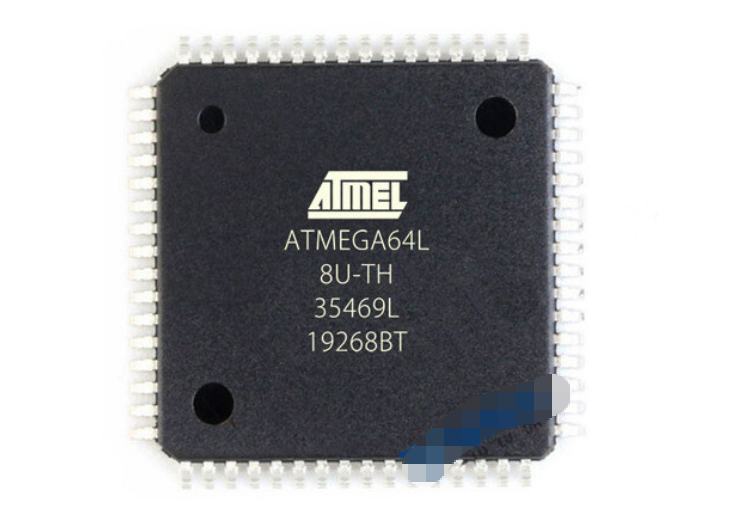
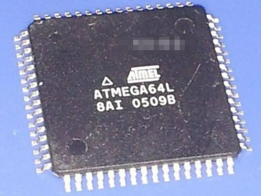
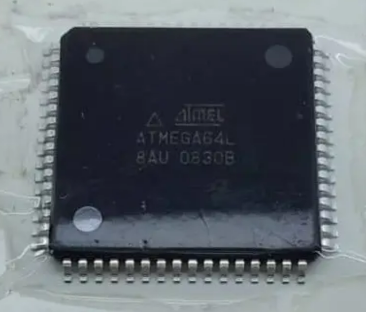
Copy Chip ATmega64L EEPROM is a specialized professional service designed for legitimate owners who need to recover, preserve, or migrate critical embedded data from legacy or active AVR-based systems. The ATmega64L is a widely adopted 8-bit microcontroller from Atmel (Microchip) known for its low-power operation, rich peripheral set, and stable architecture, making it a long-term choice in industrial control, consumer electronics, automotive modules, medical instruments, smart meters, security devices, and various customized embedded products. In many of these applications, essential configuration data, calibration parameters, device identifiers, and control logic are stored inside EEPROM, flash memory, or protected program areas, often in a locked, encrypted, or otherwise secured state.
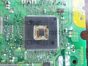
We can Copy Chip ATmega64L Eeprom, please view below chip features for your reference:
· High-performance, Low-power Atmel® CHIP® 8-bit Microcontroller
· Advanced RISC Architecture
– 130 Powerful Instructions – Most Single Clock Cycle Execution
– 32 x 8 General Purpose Working Registers + Peripheral Control Registers
– Fully Static Operation
– Up to 16 MIPS Throughput at 16 MHz
– On-chip 2-cycle Multiplier
When original firmware documentation, source code, or archived files are lost, businesses may face production stoppages, maintenance risks, or costly redesigns. Our Copy Chip ATmega64L EEPROM service helps customers legally attack these barriers at a high level, enabling them to retrieve, decode, clone, or duplicate their own embedded firmware, binary, or heximal data without revealing sensitive technical methods. The ATmega64L’s unique features—such as multiple communication interfaces, flexible memory mapping, and reliable EEPROM endurance—also introduce challenges when protection bits are enabled, as standard programmers cannot access locked memory regions. In such cases, advanced analysis may be required to break through protective mechanisms and retrieve the embedded data archive in a controlled and secure manner.
High Endurance Non-volatile Memory segments
– 64 Kbytes of In-System Reprogrammable Flash program memory
– 2 Kbytes EEPROM
– 4 Kbytes Internal SRAM
– Write/Erase Cycles: 10,000 Flash/100,000 EEPROM
– Data retention: 20 years at 85°C/100 years at 25°C(1)
– Optional Boot Code Section with Independent Lock Bits
In-System Programming by On-chip Boot Program
True Read-While-Write Operation
– Up to 64 Kbytes Optional External Memory Space
– Programming Lock for Software Security
– SPI Interface for In-System Programming
JTAG (IEEE std. 1149.1 Compliant) Interface
– Boundary-scan Capabilities According to the JTAG Standard
– Extensive On-chip Debug Support
– Programming of Flash, EEPROM, Fuses, and Lock Bits through the JTAG Interface
Peripheral Features
– Two 8-bit Timer/Counters with Separate Prescalers and Compare Modes
– Two Expanded 16-bit Timer/Counters with Separate Prescaler, Compare Mode, and Capture Mode
– Real Time Counter with Separate Oscillator
– Two 8-bit PWM Channels
– 6 PWM Channels with Programmable Resolution from 1 to 16 Bits
– 8-channel, 10-bit ADC
8 Single-ended Channels
7 Differential Channels
2 Differential Channels with Programmable Gain (1x, 10x, 200x)
– Byte-oriented Two-wire Serial Interface
– Dual Programmable Serial USARTs
– Master/Slave SPI Serial Interface
– Programmable Watchdog Timer with On-chip Oscillator
– On-chip Analog Comparator
Special Microcontroller Features
– Power-on Reset and Programmable Brown-out Detection
– Internal Calibrated RC Oscillator
– External and Internal Interrupt Sources
– Six Sleep Modes: Idle, ADC Noise Reduction, Power-save, Power-down, Standby
and Extended Standby
– Software Selectable Clock Frequency
– ATmega103 Compatibility Mode Selected by a Fuse
– Global Pull-up Disable
I/O and Packages
– 53 Programmable I/O Lines
– 64-lead TQFP and 64-pad QFN/MLF
Operating Voltages
– 2.7V – 5.5V for ATmega64L
– 4.5V – 5.5V for ATmega64
The purpose of this service is not to encourage unauthorized hack activities, but to support product lifecycle continuity, intellectual property preservation, and system recovery for authorized users. Typical use cases include restoring EEPROM data after a supplier shutdown, cloning a proven controller for small-batch manufacturing, duplicating a stable program file for backup, or migrating firmware to a newer platform while keeping original behavior intact.
During the recovery process, difficulties may arise from aging silicon, partially corrupted memory cells, undocumented firmware revisions, or deeply encrypted security configurations that require careful handling to avoid data loss. Despite these challenges, successful EEPROM and flash retrieval allows customers to rebuild their firmware archive, validate binary integrity, and securely store recovered source-level representations where applicable.
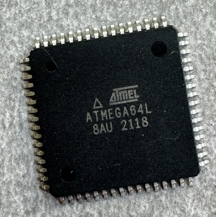
The benefits for end users include reduced downtime, lower redevelopment costs, extended product lifespan, and improved operational resilience, all while maintaining confidentiality and compliance. By delivering verified firmware, EEPROM, and memory files in usable formats, our Copy Chip ATmega64L EEPROM service provides a practical, professional solution for industries that rely on stable embedded systems and cannot afford to lose access to their secured microcontroller data.
Copy Microcontroller PIC16C76 Heximal
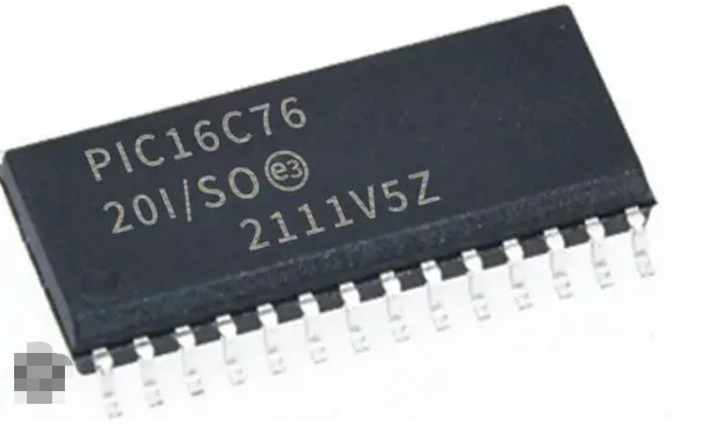
The Microchip PIC16C76 is a classic 8-bit microcontroller that continues to operate in a wide range of industrial and commercial products. When customers search for Copy Microcontroller PIC16C76 Heximal, it is usually because the original source code, program, or compiled firmware has been lost, yet the hardware remains essential to daily operations. Our professional recovery service is designed to help authorized owners retrieve, clone, or duplicate the internal heximal and binary content from protected and secured PIC16C76 devices—without exposing sensitive technical details.
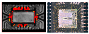
We can Copy Microcontroller PIC16C76 Heximal, please view the Microcontroller PIC16C76 features for your reference:
Any instruction which writes, operates internally as a read followed by a write operation. The BCF and BSF instructions, for example, read the register into the CPU, execute the bit operation and write the result back to the register.
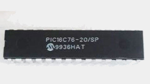
Thanks to its stable architecture, integrated peripherals, and reliable embedded design, the PIC16C76 has been widely used in:
- Industrial automation controllers and monitoring systems
- Measurement instruments and data acquisition devices
- Motor control and power management modules
- Consumer electronics and appliance controllers
- Educational platforms and OEM-specific embedded products
In these applications, critical operational logic and calibration data are stored in internal flash, EEPROM, and memory areas. Once these regions become locked or encrypted, standard programmers are unable to access the internal archive, creating major risks for maintenance and production continuity.
Caution must be used when these instructions are applied to a port with both inputs and outputs defined. For example, a BSF operation on bit5 of PORTB will cause all eight bits of PORTB to be read into the CPU.
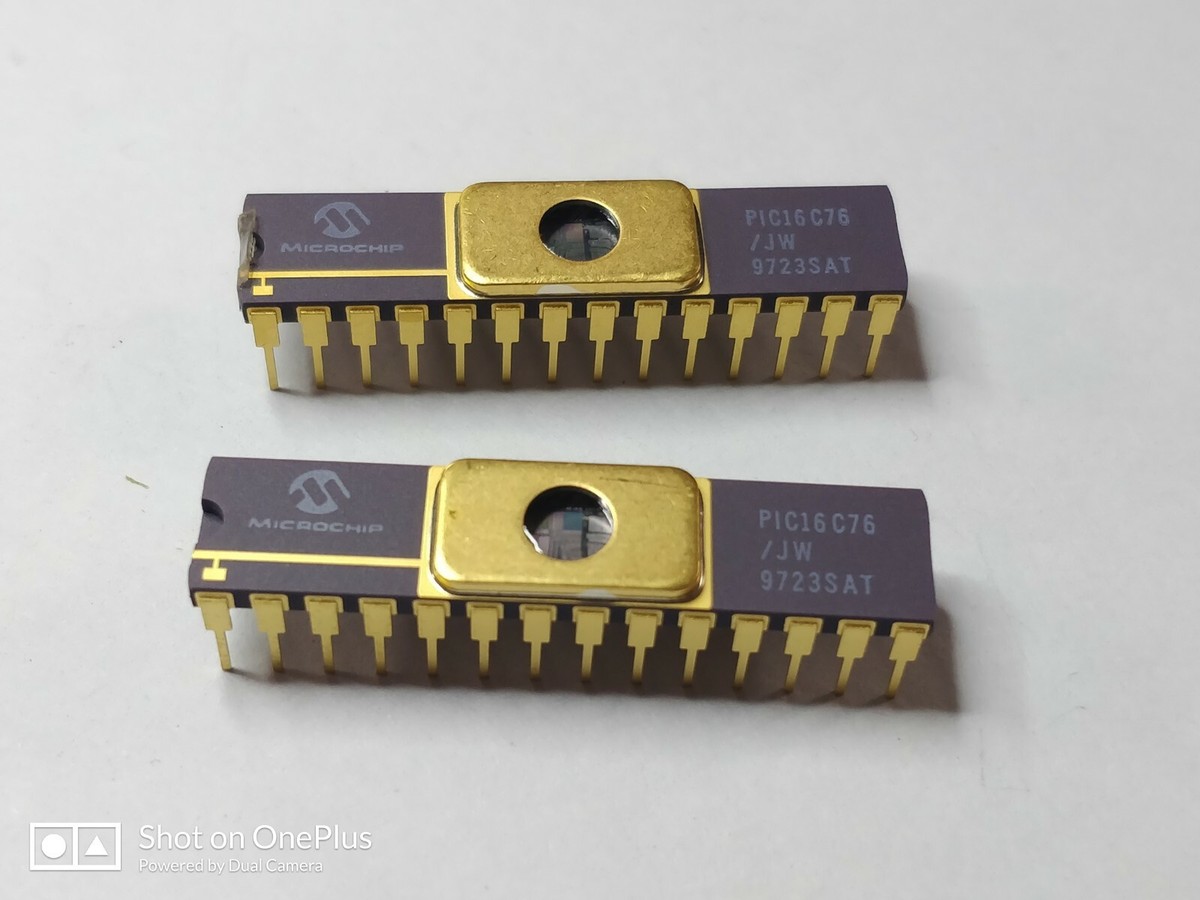
Our service supports legitimate clients who need to attack access barriers in order to recover their own intellectual property. We help customers break through protective security mechanisms and safely decode the embedded program stored within the microcontroller.
Depending on the device condition and security configuration, recovery may involve controlled analysis, advanced inspection, or authorized decapsulation. The final result is a verified file containing the recovered firmware, delivered as a binary or heximal image suitable for archiving, system migration, or controlled duplication. We do not disclose how the recovery is performed, and we do not provide instructions on how to hack devices.

Then the BSF operation takes place on bit5 and PORTB is written to the output latches. If another bit of PORTB is used as a bi-directional I/O pin (e.g., bit0) and it is defined as an input at this time, the input signal present on the pin itself would be read into the CPU and rewritten to the data latch of this particular pin, overwriting the previous content.
Organizations rely on this service for several important reasons:
- Restoring production when original source code is unavailable
- Avoiding costly redesign of proven legacy hardware
- Creating a secure archive for long-term product support
- Enabling accurate system clone or duplicate manufacturing
- Protecting existing engineering investment and operational know-how
Recovered firmware allows businesses to extend product life cycles, reduce downtime, and maintain control over their embedded systems.
As long as the pin stays in the input mode, no problem occurs. However, if bit0 is switched to an output, the content of the data latch may now be unknown.
Reading the port register, reads the values of the port pins. Writing to the port register writes the value to the port latch. When using read-modify-write instructions (ex.BCF, BSF, etc.) on a port, the value of the port pins is read, the desired operation is done to this value, and this value is then written to the port latch.
Example 5-4 shows the effect of two sequential read-modify-write instructions on an I/O port. A pin actively outputting a Low or High should not be driven from external devices at the same time in order to change the level on this pin (“wired-or”, “wired-and”). The resulting high output currents may damage the chip.
The actual write to an I/O port happens at the end of an instruction cycle, whereas for reading, the data must be valid at the beginning of the instruction cycle (Figure 5-10). Therefore, care must be exercised if a write followed by a read operation is carried out on the same I/ O port.
The sequence of instructions should be such to allow the pin voltage to stabilize (load dependent) before the next instruction which causes that file to be read into the CPU is executed. Otherwise, the previous state of that pin may be read into the CPU rather than the new state in the process of Copy Microcontroller PIC16C76 Heximal. When in doubt, it is better to separate these instructions with a NOP or another instruction not accessing this I/O port.
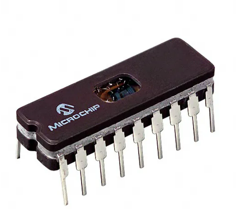
It can directly interface to an 8-bit microprocessor data bus. The external microprocessor can read or write the PORTD latch as an 8-bi t latch. Setting bit PSPMODE enables port pin RE0/RD/AN5 to be the RD input, RE1/WR/AN6 to be the WR input and RE2/CS/AN7 to be the CS (chip select) input to Crack MCU. For this functionality, the corresponding data direction bits of the TRISE register (TRISE<2:0>) must be configured as inputs (set) and the A/D port configuration bits PCFG2:PCFG0 (ADCON1<2:0>) must be set, which will configure pins RE2:RE0 as digital I/O.
Each PIC16C76 unit is first evaluated to confirm feasibility. Once approved, controlled processes are applied to retrieve internal data while preserving memory integrity. The recovered output is validated to ensure completeness and usability. Common difficulties include aging silicon, partial memory degradation, undocumented device revisions, or deeply secured configurations. These challenges require experience and precision to ensure reliable results without data loss.
Posted in Reverse Engineer Microcontroller |
Tags: copy microcontroller locked binary, copy microcontroller locked content, copy microcontroller locked data, copy microcontroller locked file, copy microcontroller locked flash, copy microcontroller locked heximal, copy microcontroller locked software, pękać mikrokontroler bin, pękać mikrokontroler code, pękać mikrokontroler data, pękać mikrokontroler eeprom, pękać mikrokontroler file, pękać mikrokontroler firmware, pękać mikrokontroler flash, pękać mikrokontroler hex, pękać mikrokontroler memory, pękać mikrokontroler program |
Comments Closed
Copy IC PIC16F84 Code
The Microchip PIC16F84 is one of the most widely recognized microcontrollers in the history of embedded design. Even today, it remains active inside countless industrial controllers, educational platforms, automation modules, access systems, and consumer electronics. When organizations search for Copy IC PIC16F84 Code, it is typically because the original source code, program, or compiled firmware has been lost, while the hardware must continue operating. Our specialized service is designed to help legitimate owners retrieve, clone, or duplicate the embedded binary or heximal content from protected devices—without exposing any technical methods.
All PICmicro™ microcontrollers employ an advanced RISC architecture. PIC16F8X devices have enhanced core features, eight-level deep stack, and multiple internal and external interrupt sources. The separate instruction and data buses of the Harvard architecture allow a 14-bit wide instruction word with a separate 8-bit wide data bus which can be used for Copy IC PIC16F84 Code. The two stage instruction pipeline allows all instructions to execute in a single cycle, except for program branches (which require two cycles). A total of 35 instructions (reduced instruction set) are available. Additionally, a large register set is used to achieve a very high performance level.
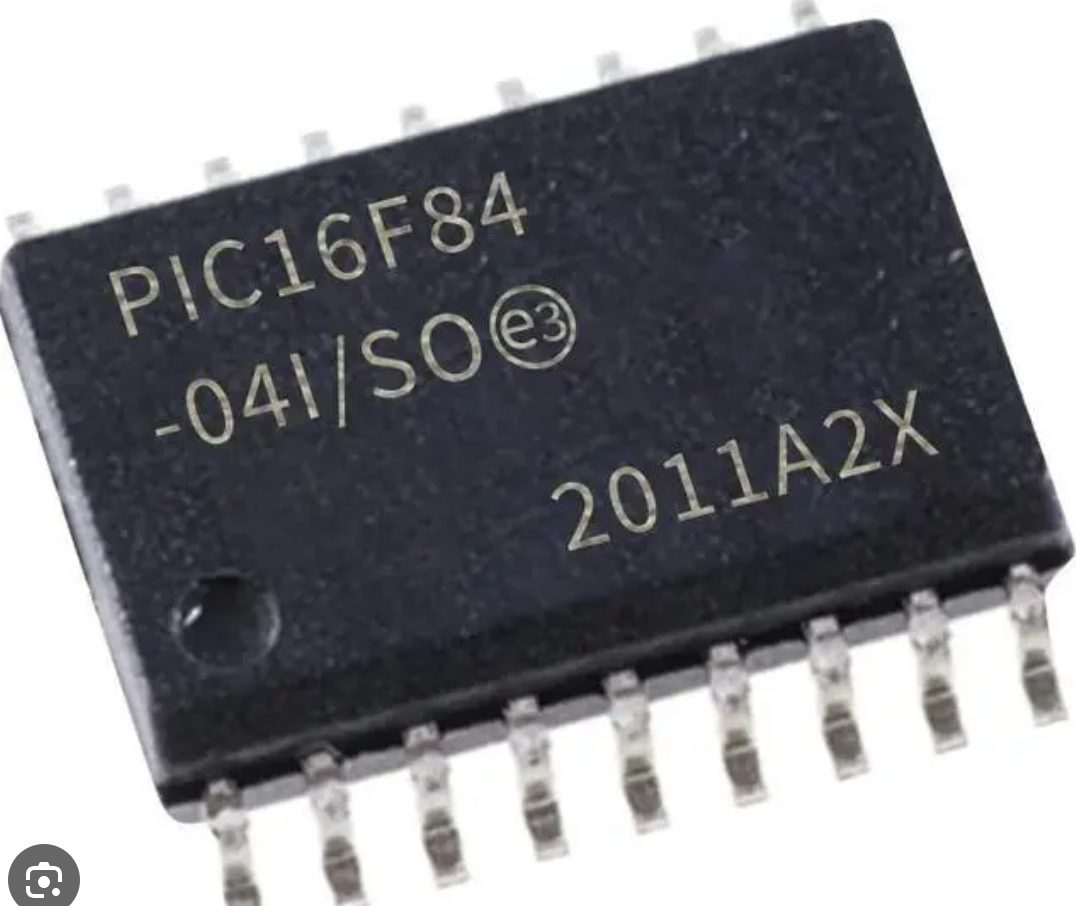
The PIC16F84 gained popularity due to its simplicity, reliability, and on-chip flash and EEPROM memory, which made it ideal for early embedded applications such as:
- Industrial automation and timing controllers
- Educational development boards and training systems
- Home appliances and basic consumer electronics
- Security alarms and access-control units
- Small robotic and sensor-based products
Its non-volatile memory allows systems to store logic and configuration data even after power loss, making the internal archive essential for maintenance and future expansion.
PIC16F8X microcontrollers typically achieve a 2:1 code compression and up to a 4:1 speed improvement (at 20 MHz) over other 8-bit microcontrollers in their class. The PIC16F8X has up to 68 bytes of RAM, 64 bytes of Data EEPROM memory, and 13 I/O pins. A timer/counter is also available.
Our service assists authorized clients who need to attack or break access restrictions imposed by locked, encrypted, or secured configurations. Standard programmers cannot decode or read these devices once protection is enabled. Through controlled analysis and, when required, approved decapsulation, we safely retrieve the internal program and reconstruct a usable file.
We do not provide instructions on how to hack devices. All processes are handled internally, and customers receive only the final recovered firmware, suitable for validation, redesign, or controlled replication.
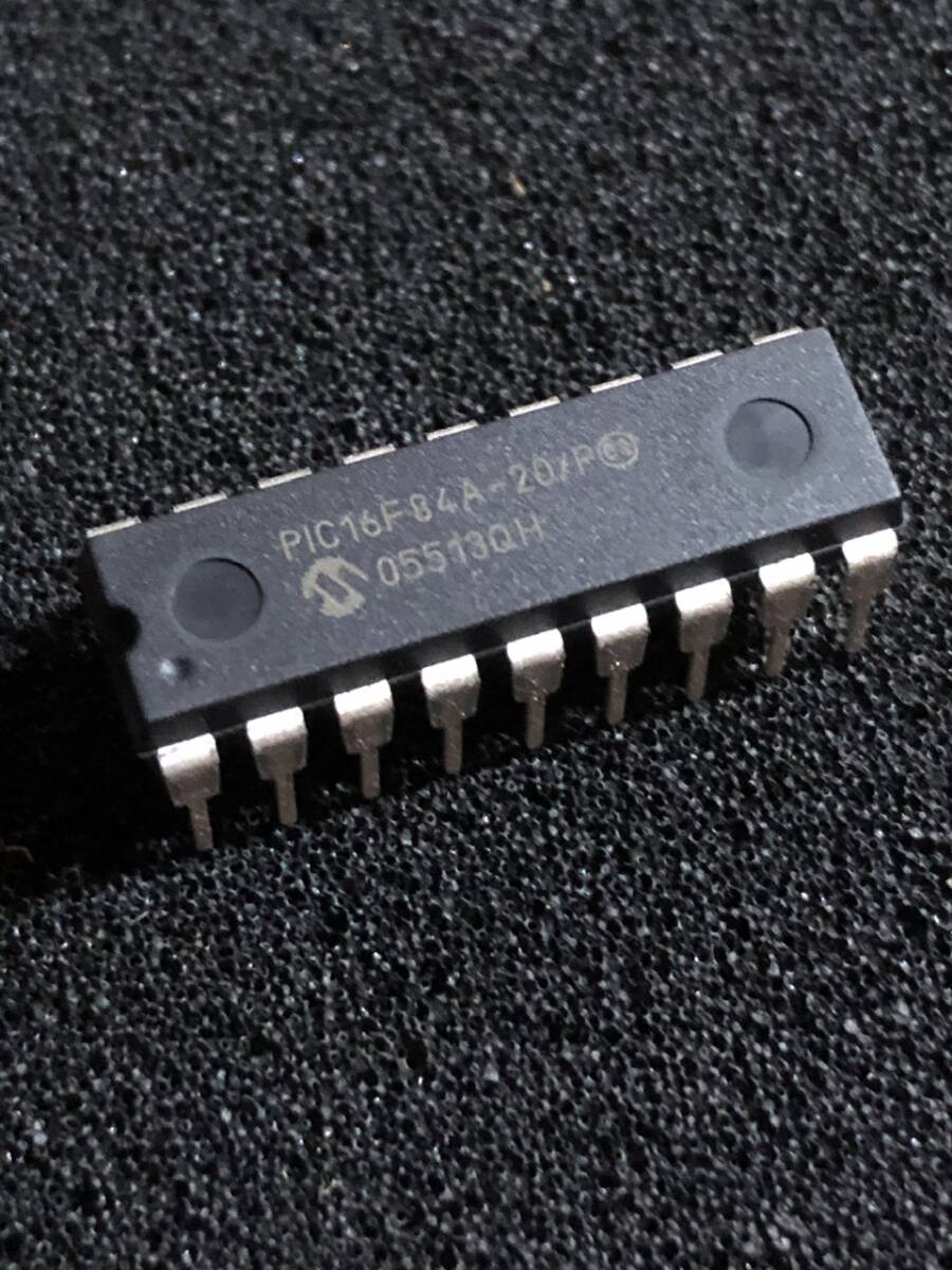
The PIC16CXX family has special features to reduce external components, thus reducing cost, enhancing system reliability and reducing power consumption.
There are four oscillator options, of which the single pin RC oscillator provides a low-cost solution, the LP oscillator minimizes power consumption, XT is a standard crystal, and the HS is for High Speed crystals.
Clients use this service to:
- Restore production when original developers are unavailable
- Avoid costly redesign of proven legacy systems
- Build verified archives for long-term product support
- Enable accurate clone or duplicate manufacturing
- Preserve intellectual property already embedded in hardware
Recovering the PIC16F84 code ensures continuity, lowers risk, and protects prior engineering investment.
The SLEEP (power-down) mode offers power saving. The user can wake the chip from sleep through several external and internal interrupts and resets. A highly reliable Watchdog Timer with its own on-chip RC oscillator provides protection against software lock-up. The devices with Flash program memory allow the same device package to be used for prototyping and production.
In-circuit reprogrammability allows the code to be updated without the device being removed from the end application. This is useful in the development of many applications where the device may not be easily accessible to Copy IC PIC16F84 Code, but the prototypes may require code updates. This is also useful for remote applications where the code may need to be updated (such as rate information).
The PIC16F8X fits perfectly in applications ranging from high speed automotive and appliance motor control to low-power remote sensors, electronic locks, security devices and smart cards. The Flash/EEPROM technology makes customization of application programs (transmitter codes, motor speeds, receiver frequencies, security codes, etc.) extremely fast and convenient.
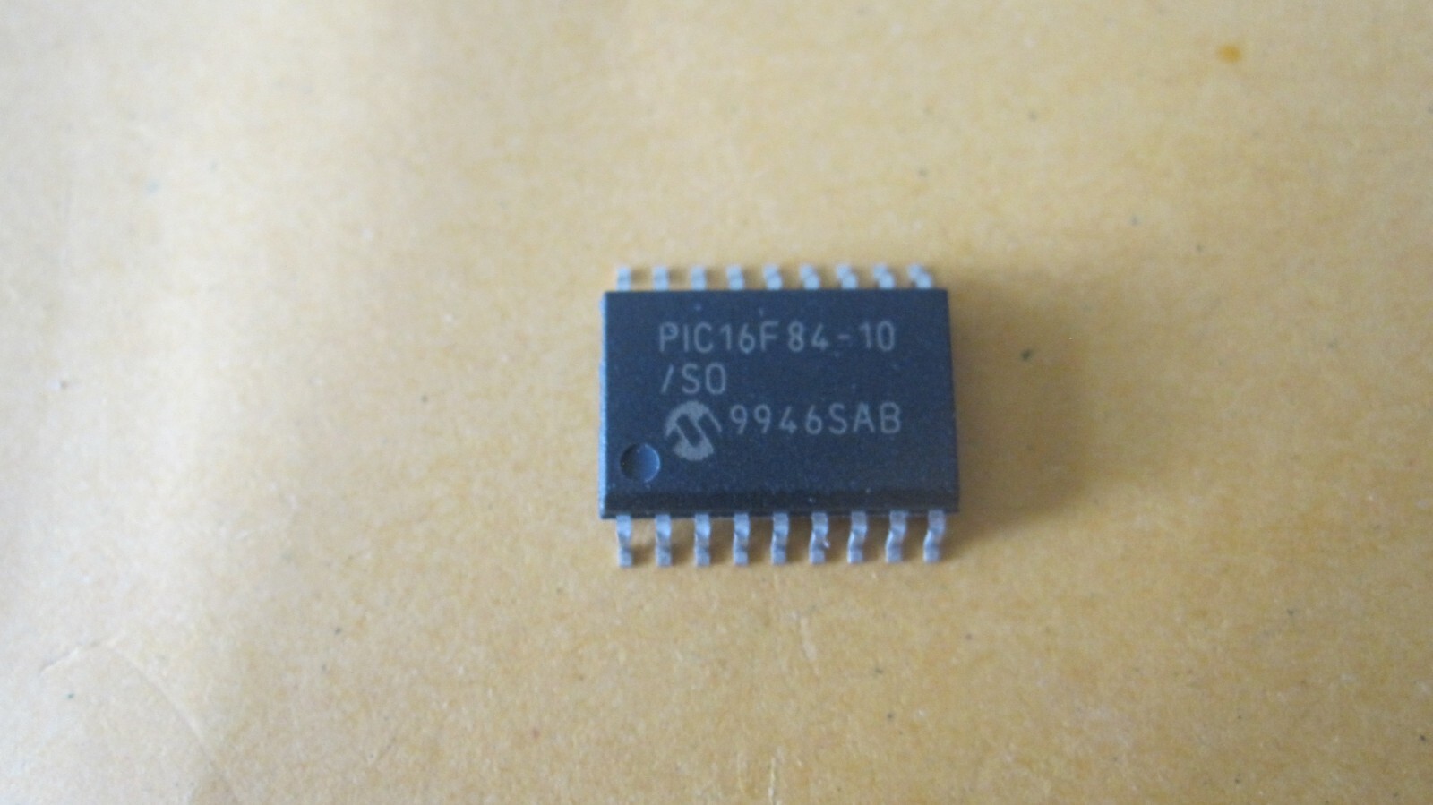
The small footprint packages make this microcontroller series perfect for all applications with space limitations. Low-cost, low-power, high performance, ease-of-use and I/O flexibility make the PIC16F8X very versatile even in areas where no microcontroller use has been considered (e.g., timer functions; serial communication; capture, compare and PWM functions; and co-processor applications).
The serial in-system programming feature (via two pins) offers flexibility of customizing the product after complete assembly and testing. This feature can be used to serialize a product, store calibration data, or program the device with the current firmware before shipping.
Typical difficulties include aging silicon, partially degraded EEPROM, undocumented revisions, or deeply protective security settings. These challenges require experience and precision to ensure complete and reliable output.
Posted in Reverse Engineer Microcontroller |
Tags: copy ic source binary, copy ic source content, copy ic source data, copy ic source file, copy ic source flash, copy ic source heximal, copy ic source software, zerwać mikrokontroler bin, zerwać mikrokontroler code, zerwać mikrokontroler data, zerwać mikrokontroler eeprom, zerwać mikrokontroler file, zerwać mikrokontroler firmware, zerwać mikrokontroler flash, zerwać mikrokontroler hex, zerwać mikrokontroler memory, zerwać mikrokontroler program |
Comments Closed