Archive for the ‘Recover MCU’ Category
 Winbond W78ERD2 MCU Locked Program Recovery
 April 11th, 2013 |
  Author:
 After the MCU has been switched to In-System Programming (ISP) Mode, Winbond W78ERD2 MCU Locked Program Recovery can be executed directly, The W78ERD2 equips one 64K byte of main MTP-ROM bank for application program (called APROM) and one 4K byte of auxiliary MTP-ROM bank for loader program (called LDROM).
In the normal operation, the microcontroller executes the code in the APROM. If the content of APROM needs to be modified, the W78ERD2 allows user to activate the In-System Programming (ISP) mode by setting the CHPCON register.
The CHPCON is read-only by default, software must write two specific values 87H, then 59H sequentially to the CHPENR register to enable the CHPCON write attribute. Writing CHPENR register with the values except 87H and 59H will close CHPCON register write attribute.
The W78ERD2 achieves all in-system programming operations including enter/exit ISP Mode, program, erase, read …etc, during device in the idle mode. Setting the bit CHPCON.0 the device will enter in-system programming mode after a wake-up from idle mode from Winbond W78ERD2 MCU Locked Program Recovery.
Because device needs proper time to complete the ISP operations before awaken from idle mode, software may use timer interrupt to control the duration for wake-up from idle mode. This in-system programming feature makes the job easy and efficient in which the application needs to update firmware frequently. In some applications, the in-system programming feature make it possible that the end-user is able to easily update the system firmware by themselves without opening the chassis.
SFRAH,SFRAL:
The objective address of on-chip MTP-ROM in the in-system programming mode. SFRFAH contains the high-order byte of address, SFRFAL contains the low-order byte of address.
SFRFD:
The programming data for on-chip MTP-ROM in programming mode.
SFRCN:
The control byte of on-chip MTP-ROM programming mode.
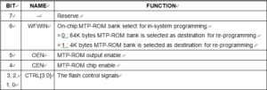
SFRCN (C7)
 Posted in
Reverse Engineering Winbond W78E354 Microcontroller
Reverse Engineering Winbond W78E354 Microcontroller
Through Power glitch method we can find an effective way to Reverse Engineering Winbond W78E354 Microcontroller and get its program and data from both eeprom and flash effortlessly, as a result of that, it is important to have some knowledge about the power management:
Idle Mode
The idle mode is entered by setting the IDL bit in the PCON register. In the idle mode, the internal clock to the processor is stopped. The peripherals and the interrupt logic continue to be clocked. The processor will exit idle mode when either an interrupt or a reset occurs.
Power-down Mode
When the PD bit in the PCON register is set, the processor enters the power-down mode. In this mode all of the clocks are stopped, including the oscillator. To exit from power-down mode is by a hardware reset or external interrupts INT0 to INT3 when enabled and set to level triggered.
Reduce EMI Emission
The W78E354 allows user to diminish the gain of on-chip oscillator amplifier by using programmer to clear the B7 bit of security register. Once B7 is set to 0, a half of gain will be decreased. Care must be taken if user attempts to diminish the gain of oscillator amplifier from Reverse Engineering Winbond W78E354 Microcontroller, reducing a half of gain may affect the external crystal operating improperly at high frequency above 24 MHz. The value of R and C1,C2 may need some adjustment while running at lower gain.
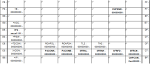
W78E354 Special Function Registers (SFRs) and Reset Values
Reset
The external RESET signal is sampled at S5P2. To take effect, it must be held high for at least two machine cycles while the oscillator is running. An internal trigger circuit in the reset line is used to deglitch the reset line when the W78E62B is used with an external RC network.
The reset logic also has a special glitch removal circuit that ignores glitches on the reset line. During reset, the ports are initialized to FFH, the stack pointer to 07H, PCON (with the exception of bit 4) to 00H, and all of the other SFR registers except SBUF to 00H. SBUF is not reset.
Attack Winbond W78E051A Protected Eeprom
When Attack Winbond W78E051A Protected Eeprom, we need to have some general idea about its architecture. The W78E051A architecture consists of a core controller surrounded by various registers, five general purpose I/O ports, 256 bytes of RAM, three timer/counters, and a serial port. The processor supports 111 different opcodes and references both a 64K program address space and a 64K data storage space.
Timers 0, 1, and 2
Timers 0, 1, and 2 each consist of two 8-bit data registers. These are called TL0 and TH0 for Timer 0, TL1 and TH1 for Timer 1, and TL2 and TH2 for Timer 2. The TCON and TMOD registers provide control functions for timers 0 and 1. The T2CON register provides control functions for Timer 2. RCAP2H and RCAP2L are used as reload/capture registers for Timer 2.
The operations of Timer 0 and Timer 1 are the same as in the W78E051A. Timer 2 is a special feature of the W78E051A: it is a 16-bit timer/counter that is configured and controlled by the T2CON register. Like Timers 0 and 1, Timer 2 can operate as either an external event counter or as an internal timer after Attack Winbond W78E051A Protected Eeprom, depending on the setting of bit C/T2 in T2CON. Timer 2 has three operating modes: capture, auto- reload, and baud rate generator. The clock speed at capture or auto-reload mode is the same as that of Timers 0 and 1.
New Defined Peripheral
In order to be more suitable for I/O, an extra 4-bit bit-addressable port P4 and two external interrupt INT2 , INT3 has been added to either the PLCC or QFP 44-pin package. And description follows:
1. INT2 / INT3
Two additional external interrupts, INT2 and INT3 , whose functions are similar to those of external interrupt 0 and 1 in the standard 80C52. The functions/status of these interrupts are determined/shown by the bits in the XICON (External Interrupt Control) register. The XICON register is bit-addressable but is not a standard register in the standard 80C52. Its address is at 0C0H. To set/clear bits in the XICON register, one can use the “SETB (/CLR) bit” instruction. For example, “SETB 0C2H” sets the EX2 bit of XICON.
Reverse Engineering Winbond W78E54B Eeprom Heximal
Reverse Engineering Winbond W78E54B Eeprom Heximal need to decapsulate the polysilicon package and get access to the chip die which will help hacker read out the heximal from its eeprom area directly.
Hereby we would like to introduce the main features of W78E54B, The W78E54B is an 8-bit microcontroller which can accommodate a wider frequency range with low power consumption. The instruction set for the W78E54B is fully compatible with the standard 8051.
The W78E54B contains an 16K bytes Flash EPROM; a 256 bytes RAM; four 8-bit bi-directional and bit- addressable I/O ports; an additional 4-bit I/O port P4; three 16-bit timer/counters; a hardware watchdog timer and a serial port. These peripherals are supported by eight sources two-level interrupt capability.
To facilitate programming and verification, the Flash EPROM inside the W78E54B allows the program memory to be programmed and read electronically after Reverse Engineering Winbond W78E54B Eeprom Heximal. Once the code is confirmed, the user can protect the code for security.
The W78E54B microcontroller has two power reduction modes, idle mode and power-down mode, both of which are software selectable. The idle mode turns off the processor clock but allows for continued peripheral operation. The power-down mode stops the crystal oscillator for minimum power consumption. The external clock can be stopped at any time and in any state without affecting the processor.
• Fully static design 8-bit CMOS microcontroller
• Wide supply voltage of 4.5V to 5.5V
• 256 bytes of on-chip scratchpad RAM
• 16 KB electrically erasable/programmable Flash EPROM
• 64 KB program memory address space
• 64 KB data memory address space
• Four 8-bit bi-directional ports
• One extra 4-bit bit-addressable I/O port, additional INT2 / INT3
(available on 44-pin PLCC/QFP package)
• Three 16-bit timer/counters
• One full duplex serial port(UART)
• Watchdog Timer
• Eight sources, two-level interrupt capability
• EMI reduction mode
• Built-in power management
• Code protection mechanism
• Packages:
DIP 40: W78E54B-24/40
PLCC 44: W78E54BP-24/40
PQFP 44: W78E54BF-24/40
Attack Nutovon Microcontroller W77E52 Flash Memory
It is very critical to reset the security bits of Microcontroller W77E52 to disable its protection against the internal memory system which include flash and eeprom, only when the bits has been disable, the Attack Nutovon Microcontroller W77E52 Flash Memory will become a possibility, now we list some of the basic features of its security bits:
During the programmer operation mode, the Flash EPROM can be programmed and verified repeatedly. Until the code inside the Flash EPROM is confirmed OK, the code can be protected. The protection of Flash EPROM and those operations on it are described below.
The W77E52 has a Special Setting Register, the Security Register, which can be accessed in normal mode. The register can only be accessed from the Flash EPROM operation mode. Those bits of the Security Registers can not be changed once they have been programmed from high to low. They can only be reset through erase-all operation. The Security Register is addressed in the Flash EPROM operation mode by address #0FFFFh when Attack Nutovon Microcontroller W77E52 Flash Memory.
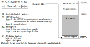
SPECIAL SETTING REGISTER
7.1 Lock Bit
This bit is used to protect the customer’s program code in the W78E51B. It may be set after the programmer finishes the programming and verifies sequence. Once this bit is set to logic 0, both the on-chip ROM data and Special Setting Registers can not be accessed again.
7.2 MOVC Inhibit
This bit is used to restrict the accessible region of the MOVC instruction. It can prevent the MOVC instruction in external program memory from reading the internal program code. When this bit is set to logic 0, a MOVC instruction in external program memory space will be able to access code only in the external memory, not in the internal memory. A MOVC instruction in internal program memory space will always be able to access the ROM data in both internal and external memory. If this bit is logic 1, there are no restrictions on the MOVC instruction after Attack Nutovon Microcontroller W77E52 Flash Memory.
7.3 Encryption
This bit is used to enable/disable the encryption logic for code protection. Once encryption feature is enabled, the data presented on port 0 will be encoded via encryption logic. Only whole chip erase will reset this bit before reverse engineering MICROCONTROLLER.
Protected Winbond Microprocessor W78E65 Reverse Engineering
The first step to get Protected Winbond Microprocessor W78E65 Reverse Engineering to get its embedded firmware include the content from both eeprom and flash is to figure out the clock frequency, as a result of that, it is critical to understand the operational procedures of Microprocessor W78E65’s clock.
The W78E51B is designed to be used with either a crystal oscillator or an external clock. Internally, the clock is divided by two before it is used.
This makes the W78E51B relatively insensitive to duty cycle variations in the clock. The W78E51B incorporates a built-in crystal oscillator. To make the oscillator work, a crystal must be connected across pins XTAL1 and XTAL2.
In addition, a load capacitor must be connected from each pin to ground. An external clock source should be connected to pin XTAL1. Pin XTAL2 should be left unconnected. The XTAL1 input is a CMOS-type input, as required by the crystal oscillator in order to finalize the evaluation of Protected Winbond Microprocessor W78E65 Reverse Engineering.
Restore Winbond Microcontroller W78E058 Heximal
We can Restore Winbond Microcontroller W78E058 Heximal, please view the Microcontroller W78E058 features for your reference:
FUNCTIONAL DESCRIPTION:
The W78E058 architecture consists of a core controller surrounded by various registers, five general purpose I/O ports, 128 bytes of RAM, two timer/counters, and a serial port. The processor supports 111 different opcodes and references both a 64K program address space and a 64K data storage space.
NEW DEFINED PERIPHERAL:
In order to be more suitable for I/O, an extra 4-bit bit-addressable port P4 and two external interrupt
INT2 , INT3 has been added to either the PLCC or QFP 44 pin package. And description follows:
INT2 / INT3
Two additional external interrupts, INT2 and INT3 , whose functions are similar to those of external interrupt 0 and 1 in the standard 80C52. The functions/status of these interrupts are determined/shown by the bits in the XICON (External Interrupt Control) register. The XICON register is bit-addressable but is not a standard register in the standard 80C52. Its address is at 0C0H. To set/clear bits in the XICON register, one can use the “SETB (/CLR) bit” instruction. For example, “SETB 0C2H” sets the EX2 bit of XICON when Restore Winbond Microcontroller W78E058 Heximal.
XICON – external interrupt control (C0H)
| PX3 | EX3 | IE3 | IT3 | PX2 | EX2 | IE2 | IT2 |
PX3: External interrupt 3 priority high if set EX3: External interrupt 3 enable if set
IE3: If IT3 = 1, IE3 is set/cleared automatically by hardware when interrupt is detected/serviced IT3: External interrupt 3 is falling-edge/low-level triggered when this bit is set/cleared by software PX2: External interrupt 2 priority high if set
EX2: External interrupt 2 enable if set
IE2: If IT2 = 1, IE2 is set/cleared automatically by hardware when interrupt is detected/serviced IT2: External interrupt 2 is falling-edge/low-level triggered when this bit is set/cleared by software after Restore Winbond Microcontroller W78E058 Heximal
Decode Winbond Chip W78E065 Internal Memory
We can Decode Winbond Chip W78E065 Internal Memory, please view the Winbond Chip W78E065 features for your reference:
The W78E065 is an 8-bit microcontroller which can accommodate a wider frequency range with low power consumption. The instruction set for the W78E065 is fully compatible with the standard 8051. The W78E065 contains an 4K bytes Flash EPROM; a 128 bytes RAM; four 8-bit bi-directional and bit- addressable I/O ports; an additional 4-bit I/O port P4; two 16-bit timer/counters; a hardware watchdog timer and a serial port.
These peripherals are supported by seven sources two-level interrupt capability. To facilitate programming and verification, the Flash EPROM inside the W78E51B allows the program memory to be programmed and read electronically. Once the code is confirmed, the user can protect the code for security when Decode Winbond Chip W78E065 Internal Memory.
The W78E065 microcontroller has two power reduction modes, idle mode and power-down mode, both of which are software selectable. The idle mode turns off the processor clock but allows for continued peripheral operation. The power-down mode stops the crystal oscillator for minimum power consumption. The external clock can be stopped at any time and in any state without affecting the processor after Decode Winbond Chip W78E065 Internal Memory.
2. FEATURES
Fully static design 8-bit CMOS microcontroller
Wide supply voltage of 4.5V to 5.5V
128 bytes of on-chip scratchpad RAM
4 KB On-chip Flash EPROM
64 KB program memory address space
64 KB data memory address space
Four 8-bit bi-directional ports
One extra 4-bit bit-addressable I/O port, additional INT2 / INT3
(available on 44-pin PLCC/QFP package)
Two 16-bit timer/counters
One full duplex serial port(UART)
Watchdog Timer
Seven sources, two-level interrupt capability
EMI reduction mode
Built-in power management
Code protection mechanism
Reverse Engineering Locked Chip ATmega164PA Firmware
We can reverse engineering locked chip ATMEGA164PA firmware, please view the locked chip ATMEGA164PA features for your reference:
The interrupt execution response for all the enabled AVR interrupts is four clock cycles minimum. After the four clock cycles the firmware vector address for the actual interrupt handling routine is executed.
During this 4-clock-cycle period, the firmware Counter (9 bits) is pushed onto the Stack. The vector is often a relative jump to the interrupt routine, and this jump takes two clock cycles.
If an interrupt occurs during execution of a multi cycle instruction, this instruction is completed before the interrupt is served. If an interrupt occurs when the MCU is in Sleep mode, the interrupt execution response time is increased by four clock cycles before Reverse Engineering Locked Chip ATmega164PA Firmware.
A return from an interrupt handling routine takes four clock cycles. During these four clock cycles, the firmware Counter (9 bits) is popped back from the Stack. When AVR exits from an interrupt, it will always return to the main firmware and execute one more instruction before any pending interrupt is served.
· Bit 7 – Res: Reserved Bit
This bit is a reserved bit in the atmega164pa and always reads as zero.
· Bit 6 – INT0: External Interrupt Request 0 Enable
When the INT0 bit is set (one) and the I-bit in the Status Register (SREG) is set (one), the external pin interrupt is activated.
The Interrupt Sense Control0 bits 1/0 (ISC01 and ISC00) in the MCU general Control Register (MCUCR) define whether the external interrupt is activated on rising or falling edge, on pin change, or low level of the INT0 pin after Reverse Engineering Locked Chip ATmega164PA Firmware.
Activity on the pin will cause an interrupt request even if INT0 is configured as an output. The corresponding interrupt of External Interrupt Request 0 is executed from firmware memory address $001. See also “External Interrupts.”
· Bit 5 – PCIE: Pin Change Interrupt Enable
When the PCIE bit is set (one) and the I-bit in the Status Register (SREG) is set (one), the interrupt on pin change is enabled. Any change on any input or I/O pin will cause an interrupt.
The corresponding interrupt of Pin Change Interrupt Request is executed from firmware memory address $002. See also “Pin Change Interrupt.”
· Bits 4..0 – Res: Reserved Bits
These bits are reserved bits in the atmega164pa and always read as zero.
· Bit 6 – INTF0: External Interrupt Flag0
When an edge or logic change on the INT0 pin triggers an interrupt request, INTF0 becomes set (one). If the I-bit in SREG and the INT0 bit in GIMSK are set (one), the MCU will jump to the interrupt vector at address $001 before Reverse Engineering Locked Chip ATmega164PA Firmware.
The flag is cleared when the interrupt routine is executed. Alternatively, the flag can be cleared by writing a logical “1” to it. The flag is always cleared when INT0 is configured as level interrupt.
· Bit 5 – PCIF: Pin Change Interrupt Flag
When an event on any input or I/O pin triggers an interrupt request, PCIF becomes set (one). If the I-bit in SREG and the PCIE bit in GIMSK are set (one), the MCU will jump to the interrupt vector at address $002.
The flag is cleared when the interrupt routine is executed. Alternatively, the flag can be cleared by writing a logical “1” to it before reverse engineering Microcontroller.
· Bits 4..0 – Res: Reserved Bits
These bits are reserved bits in the atmega164pa and always read as zero.
Recover Locked Microprocessor ATmega164PV Source Code
We can recover locked microprocessor ATMEGA164PV source code, please view the locked microprocessor ATMEGA164PV features for your reference:
To enter any of the three sleep modes, the SE bit in locked microprocessorCR must be set (one) and a SLEEP instruction must be executed. The SM1 and SM0 bits in the locked microprocessorCR register select which sleep mode (Idle, ADC Noise Reduction or Power-down) will be activated by the SLEEP instruction (see Table 7).
If an enabled interrupt occurs while the locked microprocessor is in a sleep mode, the locked microprocessor wakes up. The locked microprocessor is then halted for four cycles, executes the interrupt routine and resumes execution from the instruction following SLEEP if Recover Locked Microprocessor ATmega164PV Source Code.
On wake-up from Power-down mode on pin change, the two instructions following SLEEP. The contents of the register file, SRAM, and I/O memory are unaltered when the device wakes up from sleep.
If a reset occurs during sleep mode, the locked microprocessor wakes up and executes from the Reset vector. When the SM1/SM0 bits are “00”, the SLEEP instruction forces the locked microprocessor into the Idle mode, stopping the CPU but allowing the ADC, Analog Comparator, Timer/Counters, Watchdog and the Interrupt system to continue operating.
This enables the locked microprocessor to wake up from external triggered interrupts as well as internal ones like the Timer Overflow interrupt and Watchdog Reset. If the ADC is enabled, a conversion starts automatically when this mode is entered when Recover Locked Microprocessor ATmega164PV Source Code.
If wake-up from the Analog Comparator interrupt is not required, the Analog Comparator can be powered down by setting the ADC-bit in the Analog Comparator Control and Status Register (ACSR).
This will reduce power consumption in Idle mode. When the SM1/SM0 bits are “01”, the SLEEP instruction forces the locked microprocessor into the ADC Noise Reduction mode, stopping the CPU but allowing the ADC, the external interrupt pin, pin change interrupt and the Watchdog (if enabled) to continue operating.
Please note that the clock system including the PLL is also active in the ADC Noise Reduction mode. This improves the noise environment for the ADC, enabling higher resolution measurements after RECOVER MCU.
If the ADC is enabled, a conversion starts automatically when this mode is entered. In addition to Watchdog Time-out and External Reset, only an external leveltriggered interrupt, a pin change interrupt or an ADC interrupt can wake up.