Archive for the ‘Recover MCU’ Category
 Attack Microcontroller ST62T15C6 firmware
 April 6th, 2014 |
  Author:
 The ST62T15C6 is an 8-bit microcontroller from STMicroelectronics, commonly used in embedded systems. Security researchers and hardware hackers often attempt to attack, crack, or reverse engineer its firmware for analysis, recovery, or cloning purposes. This article explores various techniques used to extract, decode, or dump the firmware from the ST62T15C6 microcontroller.
O ST62T15C6 é um microcontrolador de 8 bits da STMicroelectronics, comumente usado em sistemas embarcados. Pesquisadores de segurança e hackers de hardware frequentemente tentam atacar, crackear ou fazer engenharia reversa em seu firmware para fins de análise, recuperação ou clonagem. Este artigo explora várias técnicas usadas para extrair, decodificar ou despejar o firmware do microcontrolador ST62T15C6.
1. Firmware Extraction Methods
Dumping Flash Memory
The primary method to attack the ST62T15C6 involves dumping the contents of its flash memory or EEPROM memory. Since the firmware is stored in non-volatile memory, attackers use hardware tools like:
- Programmers/JTAG interfaces – If debug ports are accessible, firmware can be read directly.
- Logic analyzers & bus sniffers – Monitoring communication between the MCU and external memory (if any).
- Voltage glitching – Disrupting power or clock signals to bypass read protections.
Decapsulation & Microprobing
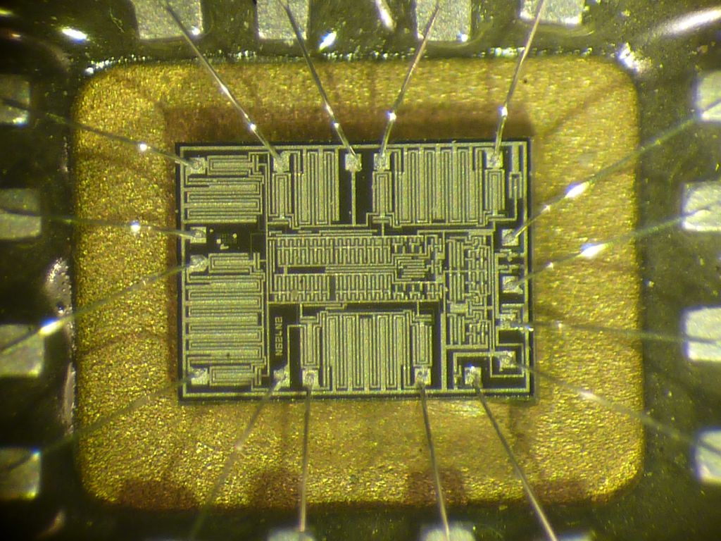
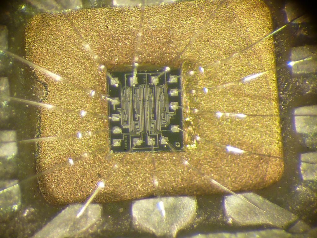
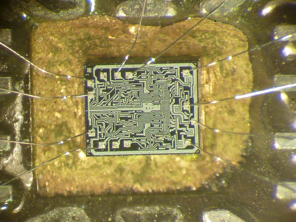
If security fuses are enabled, attackers may resort to decapsulating the chip to access the silicon die. Using microprobing, they can directly read the binary code from the memory cells. This method is expensive and requires advanced equipment.
ST62T15C6 — это 8-битный микроконтроллер от STMicroelectronics, обычно используемый во встраиваемых системах. Исследователи безопасности и хакеры оборудования часто пытаются атаковать, взломать или провести обратную разработку его прошивки для анализа, восстановления или клонирования. В этой статье рассматриваются различные методы, используемые для извлечения, декодирования или дампа прошивки из микроконтроллера ST62T15C6.
2. Reverse Engineering the Firmware
Once the heximal data or binary code is extracted, the next step is decoding or disassembling it. Common techniques include:
- Static analysis – Using disassemblers like Ghidra or IDA Pro to convert machine code into assembly.
- Dynamic analysis – Running the firmware in an emulator (e.g., QEMU) to observe behavior.
- Pattern recognition – Searching for known opcode sequences to identify functions.
Since the ST62T15C6 uses a proprietary architecture, custom tools may be needed to decrypt the program file fully.
3. Cloning & Firmware Modification
After successful extraction, attackers may:
- Copy the firmware to another ST62T15C6 chip.
- Modify the source code (if decompiled) to remove security checks.
- Restore corrupted firmware for device recovery.
4. Protection & Countermeasures
To prevent such attacks, manufacturers implement:
- Read-out protection bits – Locking firmware access.
- Encrypted firmware updates – Preventing easy decoding.
- Secure boot mechanisms – Blocking unauthorized code execution.
Conclusion
يُعد ST62T15C6 متحكمًا دقيقًا ثماني البتات من شركة STMicroelectronics، ويُستخدم عادةً في الأنظمة المدمجة. غالبًا ما يحاول باحثو الأمن ومخترقو الأجهزة مهاجمة أو اختراق أو عكس هندسة البرنامج الثابت الخاص به لأغراض التحليل أو الاستعادة أو الاستنساخ. تستكشف هذه المقالة التقنيات المختلفة المستخدمة لاستخراج أو فك تشفير أو تفريغ البرنامج الثابت من المتحكم الدقيق ST62T15C6
Attacking the ST62T15C6 microcontroller firmware requires a mix of hardware and software techniques, from dumping flash memory to reverse engineering binary code. While these methods can be used for legitimate recovery or research, they also pose security risks if exploited maliciously. Developers must implement strong protections to safeguard their firmware from unauthorized cloning or decryption.
Attack Microcontroller ST62T15C6 protective system and extract firmware from MCU ST62T15 memory, the whole tamper resistance system will be disable by Microprocessor unlocking technique
Attack Microcontroller ST62T15C6 protective system and extract firmware from MCU ST62T15 memory, the whole tamper resistance system will be disable by Microprocessor unlocking technique;
Memories
– 2K or 4K bytes Program memory (OTP, EPROM, FASTROM or ROM) with read-out protection
– 64 bytes RAM
Clock, Reset and Supply Management
– Enhanced reset system
– Low Voltage Detector (LVD) for Safe Reset
– Clock sources: crystal/ceramic resonator or RC network, external clock, backup oscillator (LFAO)
– Oscillator Safeguard (OSG)
– 2 Power Saving Modes: Wait and Stop
Interrupt Management
– 4 interrupt vectors plus NMI and RESET
– 20 external interrupt lines (on 2 vectors)
– 1 external non-interrupt line
– 20 multifunctional bidirectional I/O lines
– 16 alternate function lines
– 4 high sink outputs (20mA)
– Configurable watchdog timer
– 8-bit timer/counter with a 7-bit prescaler
Analog Peripheral
– 8-bit ADC with 16 input channels
Instruction Set
– 8-bit data manipulation
– 40 basic instructions
– 9 addressing modes
– Bit manipulation
The ST6215C, 25C devices are low cost members mable option bytes of the OTP/EPROM versions of the ST62xx 8-bit family of microcontrol-in the ROM option list applications. All ST62xx devices are based on a building block approach: a common core is surrounded by a number of on-chip peripherals for the purpose of IC program hacking.
Circuit Engineering Company Limited continues to be recognized as the Southern China Leader in Services for IC Break, MCU attack, Chip Recover, Microcontroller Copy service. With the advancement of today’s modern circuit board technology, it is more important than ever to have specialists available to help you at a moment’s notice. Our engineering and commercial teams collectively have a vast amount of electronic experience covering field include Consumer Electronics, Industrial Automation Electronics, Wireless Communication Electronics., etc. For more information please contact us through email.
 Posted in
Reverse Engineering IC Embedded Memory
Reverse Engineering IC Embedded Memory need to experience a series of complicate process, and there are a lot of methods to reverse engineering IC embedded memory, and faulty injection technology can be used to analyze the IC, because this technology can help to locate the security fuse.
Although through this reverse engineering IC technology can’t locate the exact locations of security fuse, especially when using the flash light to inject the faulty, but it is no necessary to find out its exact locations, because security fuse can be shielded after the vulnerability point being found.
The facility is very similar to the laser scanning, the only different point is the facility is flash lamp instead of laser, de-capsulate the IC and places it on the test socket of electrical automatic platform.
Expose part of IC under the flash lamp, and then test the security fuse status, and then the location of photo-sensitivity can be found, in where the security fuse can be found too. Not only the security fuse, include all of the control circuit can be sensible to the faulty injection when reverse engineering IC embedded memory which could be more difficult to locate the security fuse.
But from the perspective, it has nothing to do about it, the security evaluation can be instructed by using the same procedures from the vulnerable IC point on the channel, if then each point on the surface of IC can be used to locate the security fuse and confirm if it can be shielded under the exposure of flash lamp within a short period of time.
Through the two time scanning on the PIC16F84 microcontroller IC from microchip, the result of comparison when reverse engineering IC can find the transistors embedded in the security fuse. Although the result can be obtained within a short period of time, but there is one point need to illustrate, it has smaller effect on the small features IC and modern microcontroller IC with multilayer top metal layers. One of the optional method is through backside laser scanning which need more precise and more expensive facilities since there are more noises in the Microcontroller reverse engineering.
Decrypt Microchip PIC18F2321 MCU Heximal File
Decrypt Microchip PIC18F2321 MCU Heximal File
Inter-peripheral communication and signalling with minimum latency CPU and DMA independent operation which can affect the Decrypt Microchip PIC18F2321 MCU Heximal File
8 Event Channels allows for up to 8 signals to be routed at the same time
Events can be generated by
– Timer/Counters (TCxn)
– Real Time Counter (RTC)
– Analog to Digital Converters (ADCx)
– Analog Comparators (ACx)
– Ports (PORTx)
– System Clock (ClkSYS)
– Software (CPU)
Events can be used by secured MCU mcu reading out
– Timer/Counters (TCxn)
– Analog to Digital Converters (ADCx)
– Digital to Analog Converters (DACx)
– Ports (PORTx)
– DMA Controller (DMAC)
– IR Communication Module (IRCOM)
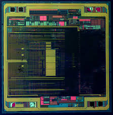
Decrypt Microchip PIC18F2321 MCU Heximal File
The same event can be used by multiple peripherals for synchronized timing
Advanced Features
– Manual Event Generation from software (CPU)
– Quadrature Decoding
– Digital Filtering
Functions in Active and Idle mode
The Event System is a set of features for inter-peripheral communication. It enables the possibility for a change of state in one peripheral to automatically trigger actions in one or more peripherals. What changes in a peripheral that will trigger actions in other peripherals are configurable by software. It is a simple, but powerful system as it allows for autonomous control of peripherals without any use of interrupts, CPU or DMA resources when MCU CRACK.
The indication of a change in a peripheral is referred to as an event, and is usually the same as the interrupt conditions for that peripheral. Events are passed between peripherals using a dedicated routing network called the Event Routing Network. Figure 9-1 on page 17 shows a basic block diagram of the Event System with the Event Routing Network and the peripherals to which it is connected.
This highly flexible system can be used for simple routing of signals, pin functions or for sequencing of events. The maximum latency is two CPU clock cycles from when an event is generated in one peripheral, until the actions are triggered in one or more other peripherals. The Event System is functional in both Active and Idle modes.
Microchip PIC18F2410 CPU Software Extraction
Microchip PIC18F2410 CPU Software Extraction
When using the DAC in S/H mode, ensure that none of the channels is running at maximum conversion rate, or ensure that the conversion rate of both channels is high enough to not require refresh. BOD will be enabled after any reset if the Microchip PIC18F2410 CPU Software Extraction can be completely properly.
If any reset source goes active, the BOD will be enabled and keep the device in reset if the VCC voltage is below the programmed BOD level. During Power-On Reset, reset will not be released until VCC is above the programmed BOD level even if the BOD is disabled.
Problem fix/Workaround
Do not set the BOD level higher than VCC even if the BOD is not used.
Both DFLLs and both oscillators has to be enabled for one to work
In order to use the automatic runtime calibration for the 2 MHz or the 32MHz internal oscillators, the DFLL for both oscillators and both oscillators has to be enabled for one to work.
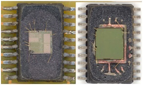
Microchip PIC18F2410 CPU Software Extraction
Problem fix/Workaround
Enabled both the DFLLs and both oscillators when using automtics runtime calibartion for one of the internal oscillators.
Operating Frequancy and Voltage Limitation
To ensure correct operation, there is a limit on operating frequnecy and voltage. Figure 36-2 on page 95 shows the safe operating area on Microchip PIC18F2410 CPU Software Extraction.
Bandgap voltage input for the ACs cannot be changed when used for both ACs simultaneously
ADC gain stage output range is limited to 2.4V
Sampled BOD in Active mode will cause noise when bandgap is used as reference
Bandgap measurement with the ADC is non-functional when VCC is below 2.7V
BOD will be enabled after any reset
Writing EEPROM or Flash while reading any of them will not work after the ADC has increased INL error for some operating conditions DAC has increased INL or noise for some operating conditions VCC voltage scaler for AC is non-linear Maximum operating frequency below 1.76V is 8 MHz.
Decrypt PIC18F2420 MCU Encrypted Program
Decrypt PIC18F2420 MCU Encrypted Program
Sampled BOD in Active mode will cause noise when bandgap is used as reference
Bandgap measurement with the ADC is non-functional when VCC is below 2.7V otherwise the procedures of Decrypt PIC18F2420 MCU encrypted Program will be paused.
BOD will be enabled after any reset
Writing EEPROM or locked while unlocking any of them will not work
ADC has increased INL error for some operating conditions
DAC has increased INL or noise for some operating conditions
VCC voltage scaler for AC is non-linear
Maximum operating frequency below 1.76V is 8 MHz
Bandgap voltage input for the ACs cannot be changed when used for both ACs simultaneously
If the bandgap voltage is selected as input for one Analog Comparator (AC) and then selected/deselected as input for the another AC, the first comparator will be affected for up to 1 us and could potentially give a wrong comparison result after the locked of chip being unlocked.
Problem fix/Workaround
If the Bandgap is required for both ACs simultaneously, configure the input selection for both ACs before enabling any of them.
ADC gain stage output range is limited to 2.4 V
The amplified output of the ADC gain stage will never go above 2.4 V, hence the differential input will only give correct output when below 2.4 V/gain. For the available gain settings, this gives a differential input range of:
Problem fix/Workaround
Keep the amplified voltage output from the ADC gain stage below 2.4 V in order to get a correct result, or keep ADC voltage reference below 2.4 V.
Sampled BOD in Active mode will cause noise when bandgap is used as reference
Using the BOD in sampled mode when the device is running in Active or Idle mode will add noise on the bandgap reference for ADC, DAC and Analog Comparator after the chip’s locked can be unlocked.
Problem fix/Workaround
If the bandgap is used as reference for either the ADC, DAC and Analog Comparator, the BOD must not be set in sampled mode.
Bandgap measurement with the ADC is non-functional when VCC is below 2.7V
The ADC cannot be used to do bandgap measurements when VCC is below 2.7V.
Problem fix/Workaround
If internal voltages must be measured when VCC is below 2.7V, measure the internal 1.00V reference instead of the bandgap.
BOD will be enabled after any reset from Decrypt PIC18F2420 MCU encrypted Program
If any reset source goes active, the BOD will be enabled and keep the device in reset if the VCC voltage is below the programmed BOD level. During Power-On Reset, reset will not be released until VCC is above the programmed BOD level even if the BOD is disabled before unlock chip data.
Problem fix/Workaround
Do not set the BOD level higher than VCC even if the BOD is not used.
Readout DSP Chip TMS320LF2406APZAR Program
The tms320lf2406apzar is a high-performance dsp device from texas instrument that has been widely used in industrial and commercial control applications requiring fast signal processing, accurate real-time calculation, and reliable embedded operation. As a specialized microprocessor platform, this chip provides strong processing capability for applications such as motor control systems, industrial automation equipment, power conversion devices, robotics, medical instruments, communication systems, and intelligent measurement platforms.
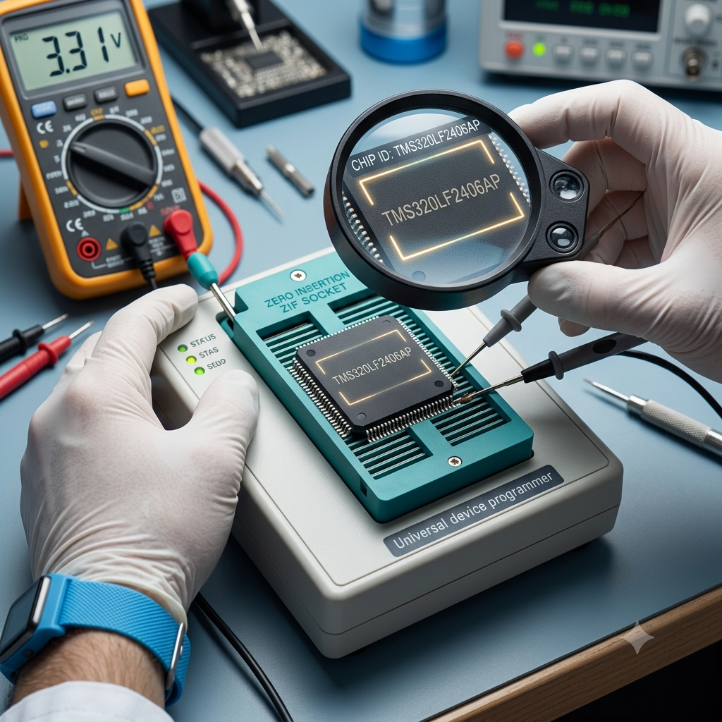
Unlike conventional microcontroller solutions, this dsp architecture is optimized for mathematical operations, digital signal processing, and complex control algorithms. During product development, manufacturers store essential firmware, control program logic, calibration data, and configuration information inside internal memory, including flash and other non-volatile storage areas. Over time, many organizations face challenges when original development documents, software projects, or engineering archive files are unavailable. Additionally, stored resources may be configured with protective, protected, locked, secured, or encrypted mechanisms, making access to original binary, heximal, and source code resources difficult without professional analysis.
High-Performance Static CMOS Technology
− 25-ns Instruction Cycle Time (40 MHz)
− 40-MIPS Performance
− Low-Power 3.3-V Design
D Based on TMS320C2xx DSP CPU Core
− Code-Compatible With F243/F241/C242
− Instruction Set and Module Compatible
With F240
D Flash (LF) and ROM (LC) Device Options
− LF240xA: LF2407A, LF2406A,
LF2403A, LF2402A
− LC240xA: LC2406A, LC2404A,
LC2403A, LC2402A
D On-Chip Memory
− Up to 32K Words x 16 Bits of Flash
EEPROM (4 Sectors) or ROM
− Programmable “Code-Security” Feature for the On-Chip Flash/ROM
− Up to 2.5K Words x 16 Bits of
Data/Program RAM
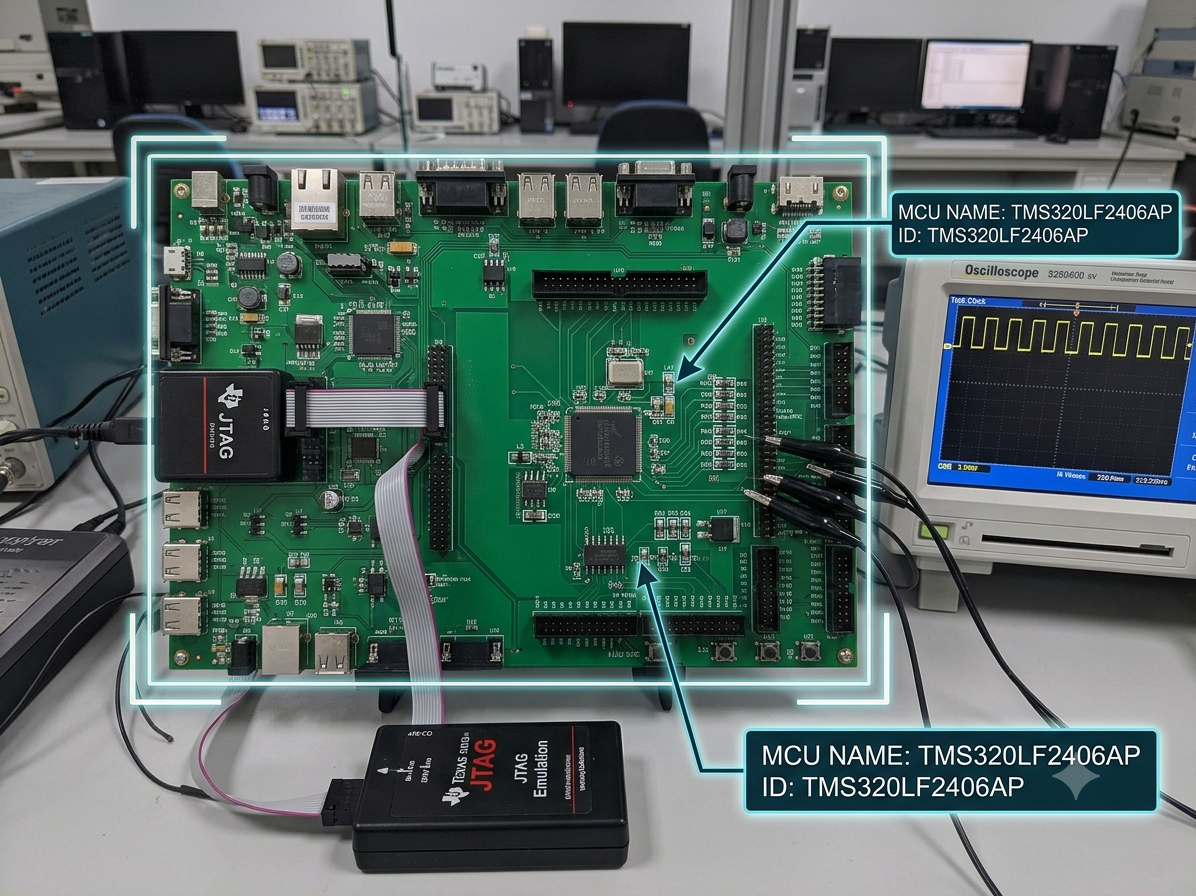
− 544 Words of Dual-Access RAM
− Up to 2K Words of Single-Access RAM
D Boot ROM (LF240xA Devices)
− SCI/SPI Bootloader
D Up to Two Event-Manager (EV) Modules (EVA and EVB), Each Includes:
− Two 16-Bit General-Purpose Timers
− Eight 16-Bit Pulse-Width Modulation (PWM) Channels Which Enable:
− Three-Phase Inverter Control
− Center- or Edge-Alignment of PWM Channels
− Emergency PWM Channel Shutdown With External PDPINTx Pin
− Programmable Deadband (Deadtime) Prevents Shoot-Through Faults
− Three Capture Units for Time-Stamping of External Events
− Input Qualifier for Select Pins
− On-Chip Position Encoder Interface Circuitry
− Synchronized A-to-D Conversion
− Designed for AC Induction, BLDC,
Switched Reluctance, and Stepper Motor Control
− Applicable for Multiple Motor and/or Converter Control
D External Memory Interface (LF2407A)
− 192K Words x 16 Bits of Total Memory:
64K Program, 64K Data, 64K I/O
D Watchdog (WD) Timer Module
D 10-Bit Analog-to-Digital Converter (ADC)
− 8 or 16 Multiplexed Input Channels
− 500-ns MIN Conversion Time
− Selectable Twin 8-State Sequencers
Triggered by Two Event Managers
D Controller Area Network (CAN) 2.0B Module (LF2407A, 2406A, 2403A)
D Serial Communications Interface (SCI)
D 16-Bit Serial Peripheral Interface (SPI)
(LF2407A, 2406A, LC2404A, 2403A)
D Phase-Locked-Loop (PLL)-Based Clock Generation
D Up to 40 Individually Programmable,
Multiplexed General-Purpose Input / Output (GPIO) Pins
D Up to Five External Interrupts (Power Drive Protection, Reset, Two Maskable Interrupts)
D Power Management:
− Three Power-Down Modes
− Ability to Power Down Each Peripheral Independently
D Real-Time JTAG-Compliant Scan-Based Emulation, IEEE Standard 1149.1† (JTAG)
D Development Tools Include:
− Texas Instruments (TI) ANSI C Compiler,
Assembler/ Linker, and Code Composer
Studio Debugger
− Evaluation Modules
− Scan-Based Self-Emulation (XDS510)
− Broad Third-Party Digital Motor Control Support D Package Options
Our “readout dsp chip tms320lf2406apzar program” service provides specialized support for authorized recovery, preservation, and analysis of valuable embedded software assets stored inside this advanced dsp platform. Through comprehensive semiconductor evaluation and firmware analysis methods, our engineers can examine the internal structure of the microprocessor, identify stored program resources, and assist in recovering available firmware, data, and memory information. Depending on the device condition and project requirements, advanced laboratory procedures, including controlled decapsulate analysis, may be used to gain deeper understanding of internal storage structures.
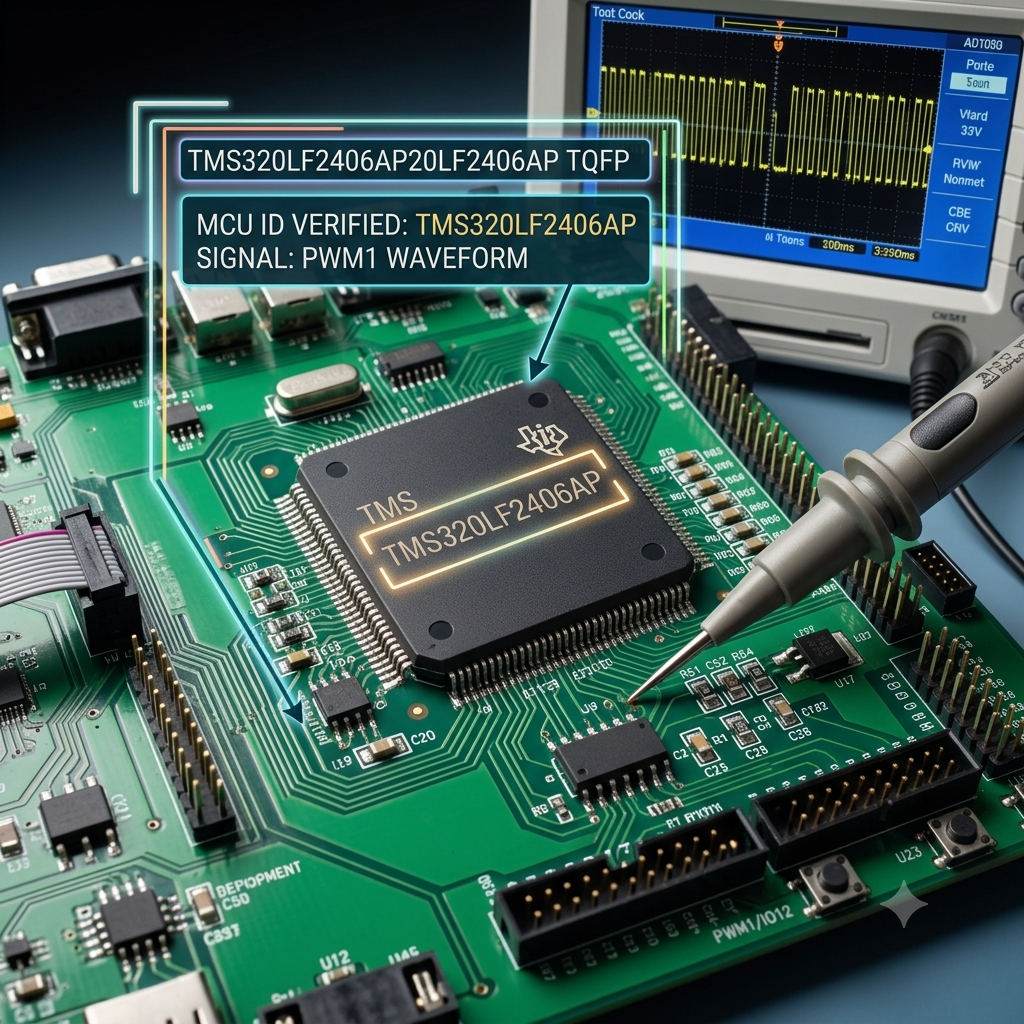
By combining hardware investigation with software interpretation, our team can retrieve available binary images, organize heximal information, and reconstruct meaningful file and archive records. Professional decode processes help transform collected information into structured engineering resources, allowing customers to analyze original firmware behavior and preserve important technical knowledge. For projects involving locked, secured, or encrypted devices, our specialists evaluate the architecture of the target texas instrument dsp and determine suitable recovery approaches. Rather than simply attempting to attack, break, or hack a device, the objective is to preserve customer-owned technology and support engineering continuity. Recovered resources may assist with product maintenance, compatibility studies, controlled clone development, and duplicate validation for legacy systems.
The recovery and analysis workflow for the tms320lf2406apzar requires a combination of dsp expertise, embedded software knowledge, and semiconductor understanding. Engineers first evaluate the condition of the chip, study the relationship between hardware operation and stored memory content, and identify the organization of available flash, firmware, and configuration regions. Extracted binary and heximal information is carefully analyzed to reconstruct meaningful program structures and support the creation of updated engineering documentation.
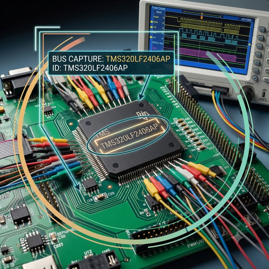
Advanced tools are used to decode recovered data, compare firmware behavior, and identify relationships between application logic and hardware functions. When authorized and technically appropriate, specialized inspection techniques, including selective decapsulate procedures, can provide additional visibility into internal structures of the mcu and microcontroller environments. This process allows engineers to recover valuable information from aging electronic systems where original software files, development environments, or source documentation may no longer exist. The final recovered archive, firmware resources, and technical records provide practical support for redesign, troubleshooting, modernization, and long-term product lifecycle management.
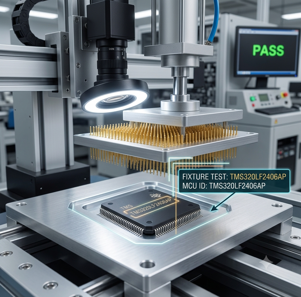
For manufacturers, engineering companies, and maintenance providers, recovering the tms320lf2406apzar program delivers significant advantages in preserving existing investments. Access to historical firmware, validated binary resources, reconstructed source code references, and organized data archives helps reduce redevelopment costs and extend the operational life of proven products.
Companies can maintain legacy control systems, support discontinued equipment, migrate designs to updated platforms, and improve technical documentation without starting development again from zero. With professional experience in dsp, texas instrument, microprocessor, and embedded microcontroller analysis, our service provides a reliable pathway for recovering valuable engineering assets and transforming inaccessible chip information into practical resources for future innovation and system continuity.
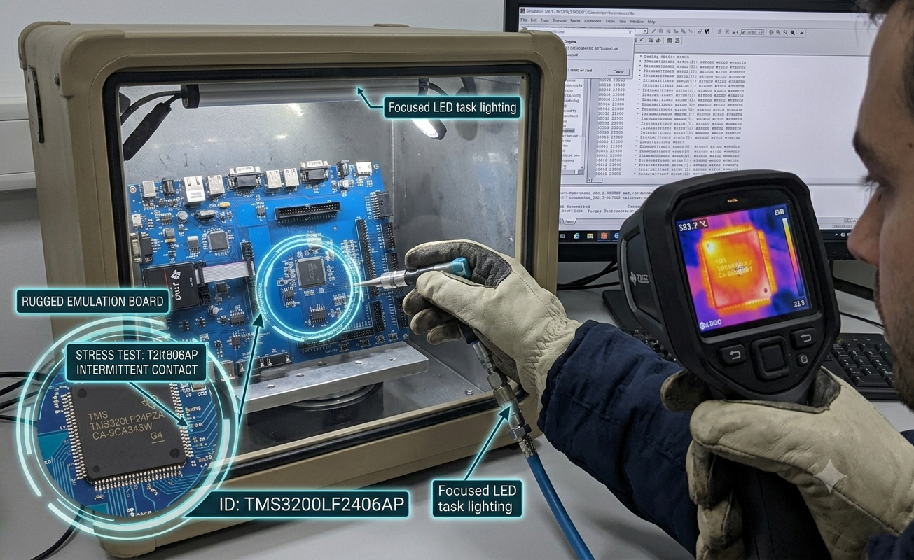
Microchip MCU PIC16F870 Heximal Code Restoration
Microchip MCU PIC16F870 Heximal Code Restoration
The content from original PIC16F870 can be re-attained through Microchip MCU PIC16F870 Heximal Code Restoration procedures:
Microcontroller Core Features:
· High performance RISC CPU
· Only 35 single word instructions to learn
· All single cycle instructions except for program branches which are two-cycle
· Operating speed: DC – 20 MHz clock input DC – 200 ns instruction cycle
· 2K x 14 words of FLASH Program Memory
128 x 8 bytes of Data Memory (RAM) 64 x 8 bytes of EEPROM Data Memory
· Pinout compatible to the PIC16CXXX 28 and 40-pin devices
· Interrupt capability (up to 11 sources)
· Eight level deep hardware stack
· Direct, Indirect and Relative Addressing modes
· Power-on Reset (POR)
· Power-up Timer (PWRT) and Oscillator Start-up Timer (OST)
· Watchdog Timer (WDT) with its own on-chip RC oscillator for reliable operation
· Programmable code protection
· Power saving SLEEP mode
· Selectable oscillator options
· Low power, high speed CMOS FLASH/EEPROM technology
· Fully static design
· In-Circuit Serial Programmingä (ICSPä) via two pins
· Single 5V In-Circuit Serial Programming capability
· In-Circuit Debugging via two pins
· Processor read/write access to program memory
· Wide operating voltage range: 2.0V to 5.5V
· High Sink/Source Current: 25 mA
· Commercial and Industrial temperature ranges
· Low power consumption:
– < 1.6 mA typical @ 5V, 4 MHz
– 20 mA typical @ 3V, 32 kHz
– < 1 mA typical standby current
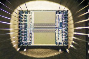
Microchip MCU PIC16F870 Heximal Code Restoration
Peripheral Features:
· Timer0: 8-bit timer/counter with 8-bit prescaler
· Timer1: 16-bit timer/counter with prescaler, can be incremented during SLEEP via external crystal/clock
· Timer2: 8-bit timer/counter with 8-bit period register, prescaler and postscaler
· One Capture, Compare, PWM module
– Capture is 16-bit, max. resolution is 12.5 ns
– Compare is 16-bit, max. resolution is 200 ns
– PWM max. resolution is 10-bit
· 10-bit multi-channel Analog-to-Digital converter
· Universal Synchronous Asynchronous Receiver
Transmitter (USART/SCI) with 9-bit address detection
· Parallel Slave Port (PSP) 8-bits wide, with external RD, WR and CS controls (40/44-pin only)
· Brown-out detection circuitry for Brown-out Reset (BOR)
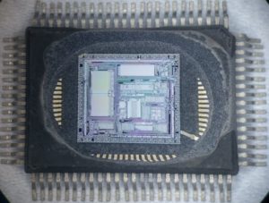
Reverse Engineering Microchip PIC16F1913 Memory
Reverse Engineering Microchip PIC16F1913 Memory
Reverse Engineering Microchip PIC16F1913 Memory means delayer the silicon, plastic and metal layer from PIC16F1913 and counter sequence of microcontroller manufacturing:
High-Performance RISC CPU:
· Only 35 instructions to learn:
– All single-cycle instructions except branches
· Operating speed:
– DC – 20 MHz oscillator/clock input
– DC – 200 ns instruction cycle
· Program Memory Read (PMR) capability
· Interrupt capability
· 8-level deep hardware stack
· Direct, Indirect and Relative Addressing modes
Special Microcontroller Features:
· Precision Internal Oscillator:
– Factory calibrated to ±1%, typical
– Software selectable frequency range of
8 MHz to 125 kHz
– Software tunable
– Two-Speed Start-up mode
– External Oscillator fail detect for critical applications
– Clock mode switching during operation for power savings
· Software selectable 31 kHz internal oscillator
· Power-Saving Sleep mode
· Wide operating voltage range (2.0V-5.5V)
· Industrial and Extended temperature range
· Power-on Reset (POR)
· Power-up Timer (PWRT) and Oscillator Start-up
Timer (OST)
· Brown-out Reset (BOR) with software control option
· Enhanced Low-Current Watchdog Timer (WDT) with on-chip oscillator (software selectable nominal 268 seconds with full prescaler) with software enable
· Multiplexed Master Clear with pull-up/input pin
· Programmable code protection
· High-Endurance Flash/EEPROM cell:
– 100,000 write Flash endurance
– 1,000,000 write EEPROM endurance
– Flash/Data EEPROM retention: > 40 years
Low-Power Features:
· Standby Current:
– <100 nA @ 2.0V, typical
· Operating Current:
– 11 ìA @ 32 kHz, 2.0V, typical
– 220 ìA @ 4 MHz, 2.0V, typical
· Watchdog Timer Current:
– 1 ìA @ 2.0V, typical
Reverse Engineering Microchip PIC16F1913 Memory
Peripheral Features:
· Liquid Crystal Display module:
– Up to 60/96/168 pixel drive capability on 28/40/64-pin devices, respectively
– Four commons
· Up to 24/35/53 I/O pins and 1 input-only pin:
– High-current source/sink for direct LED drive
– Interrupt-on-change pin
– Individually programmable weak pull-ups
· In-Circuit Serial Programming™ (ICSP™) via two pins if Reverse Engineering Microchip PIC16F1913 Memory
· Analog comparator module with:
– Two analog comparators
– Programmable on-chip voltage reference (CVREF) module (% of VDD)
– Comparator inputs and outputs externally accessible
· A/D Converter:
– 10-bit resolution and up to 8 channels
· Timer0: 8-bit timer/counter with 8-bit programmable prescaler
· Enhanced Timer1:
– 16-bit timer/counter with prescaler
– External Timer1 Gate (count enable)
– Option to use OSC1 and OSC2 as Timer1 oscillator if INTOSCIO or LP mode is selected
· Timer2: 8-bit timer/counter with 8-bit period register, prescaler and postscaler
· Addressable Universal Synchronous
Asynchronous Receiver Transmitter (AUSART)
· Up to 2 Capture, Compare, PWM modules:
– 16-bit Capture, max. resolution 12.5 ns
– 16-bit Compare, max. resolution 200 ns
– 10-bit PWM, max. frequency 20 kHz
· Synchronous Serial Port (SSP) with I2C™
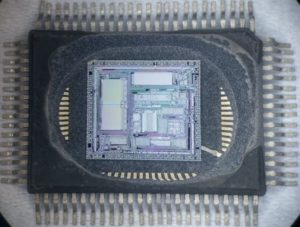
Recover TI MSP430G2452 Embedded Memory
Recover TI MSP430G2452 Embedded Memory
Recover TI MSP430G2452 Embedded Memory starts from acquiring its basic structure:
FEATURES
Low Supply Voltage Range: 1.8 V to 3.6 V
Ultra-Low Power Consumption
– Active Mode: 220 µA at 1 MHz, 2.2 V
– Standby Mode: 0.5 µA
– Off Mode (RAM Retention): 0.1 µA
Five Power-Saving Modes
Ultra-Fast Wake-Up From Standby Mode in Less Than 1 µs
16-Bit RISC Architecture, 62.5-ns Instruction Cycle Time
Recover TI MSP430G2452 Embedded Memory
Basic Clock Module Configurations
– Internal Frequencies up to 16 MHz With Four Calibrated Frequencies
– Internal Very-Low-Power Low-Frequency (LF) Oscillator
– 32-kHz Crystal
– External Digital Clock Source One 16-Bit Timer_A With Three Capture/Compare Registers
Up to 16 Touch-Sense Enabled I/O Pins
Universal Serial Interface (USI) Supporting SPI and I2C
recover MCU IC Texas Instruments MSP430G2452IPW14R
recover MCU IC Texas Instruments MSP430G2452IPW14R
10-Bit 200-ksps Analog-to-Digital (A/D)
Converter With Internal Reference, Sample-and-Hold, and Autoscan (MSP430G2x52 Only)
On-Chip Comparator for Analog
Brownout Detector Serial Onboard Programming,
No External Programming Voltage Needed,
Programmable Code Protection by Security Fuse
On-Chip Emulation Logic With Spy-Bi-Wire Interface
Family Members are Summarized in Table 1 Package Options
– TSSOP: 14 Pin, 20 Pin
– PDIP: 20 Pin
– QFN: 16 Pin
For Complete Module Descriptions, See the MSP430x2xx Family User’s Guide (SLAU144)
Restore Winbond W78IE54 MCU Encrypted Heximal
Restore Winbond W78IE54 MCU Encrypted Heximal
As we all know that in the common situation, the status of a MCU W78IE54 will be set as encrypted, and only through disable the security fuse bit can Restore Winbond W78IE54 MCU Encrypted Heximal. hereby we would like to introduce the security system of W78IE54:
During the on-chip MTP-ROM programming mode, the MTP-ROM can be programmed and verified repeatedly. Until the code inside the MTP-ROM is confirmed OK, the code can be protected. The protection of MTP-ROM and those operations on it are described below.
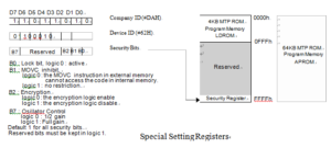
special setting register
The W78IE54 has several Special Setting Registers, including the Security Register and Company/Device ID Registers, which can not be accessed in programming mode before Restore Winbond W78IE54 MCU Encrypted Heximal. Those bits of the Security Registers can not be changed once they have been programmed from high to low.
They can only be reset through erase-all operation. The contents of the Company ID and Device ID registers have been set in factory. The Security Register is located at the 0FFFFH of the LDROM space.
Lock bit
This bit is used to protect the customer’s program code in the W78E62B. It may be set after the programmer finishes the programming and verifies sequence. Once this bit is set to logic 0, both the MTP ROM data and Special Setting Registers can not be accessed again.