 Copy CPLD IC Code
 May 2nd, 2013 |
  Author:
 Copy CPLD IC Code from CPLD chip memory is a reverse CPLD manufacturing process, original master CPLD will be cracked and firmware inside memory of CPLD can be readout directly;
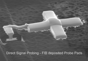
Copy CPLD IC Code from CPLD chip memory is a reverse CPLD manufacturing process, original master CPLD will be cracked and firmware inside memory of CPLD can be readout directly
Normally, the programming of an EPROM memory is controlled by external signals and all the timings should be supplied by a programmer unit. This gives an opportunity for the attacker to inject charge into the floating gate thus shifting the threshold level enough to read the memory contents when the security fuse is inactive.
Such a trick is virtually impossible to apply to modern EEPROM and Flash memory devices for several reasons. First, the programming is fully controlled by the on-chip hardware circuit. Second, the programming of EEPROM and Flash cells is normally performed by using much faster Fowler-Nordheim tunnelling rather than CHE injection. As a result it is very hard to control the exact amount of charge being placed into the cell. Also, the temperature and the supply voltage affect this process making it even harder to control.
Copy CPLD MCU Software Data
Copy CPLD MCU Software Data from flash memory and rewrite the program to new CPLD chip which can provide the same functions as original CPLD chip after MCU Cracking;
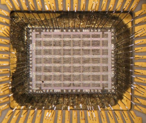
Copy CPLD MCU Software Data from flash memory and rewrite the program to new CPLD chip which can provide the same functions as original CPLD chip after MCU Cracking
There is another trick that makes recovery of memory contents possible, even when there is no overlap between the erased security fuse and non-corrupted memory content at the time of erasure. For example, we found that newer samples of the same chip will start to corrupt the memory before the security fuse is erased. In this case a power glitch cannot be used to recover information from the memory. What can be done instead is a careful adjustment of the threshold voltage in the cell’s transistor. It is possible to inject a certain portion of charge into the floating gate by carefully controlling the memory programming time.
Extract AVR Chip Software & Data
Extract AVR Chip Software Data, the program from flash memory and data from eeprom can be readout from AVR MCU after unlock AVR microcontroller protective fuse bit;
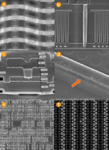
Extract AVR Chip Software & Data, the program from flash memory and data from eeprom can be readout from AVR MCU after unlock AVR microcontroller protective fuse bit
There is another trick that makes recovery of memory contents possible, even when there is no overlap between the erased security fuse and non-corrupted memory content at the time of erasure. For example, we found that newer samples of the same chip will start to corrupt the memory before the security fuse is erased. In this case a power glitch cannot be used to recover information from the memory.
What can be done instead is a careful adjustment of the threshold voltage in the cell’s transistor. It is possible to inject a certain portion of charge into the floating gate by carefully controlling the memory programming time. Normally, the programming of an EPROM memory is controlled by external signals and all the timings should be supplied by a programmer unit.
This gives an opportunity for the attacker to inject charge into the floating gate thus shifting the threshold level enough to read the memory contents when the security fuse is inactive. Such a trick is virtually impossible to apply to modern EEPROM and Flash memory devices for several reasons. First, the programming is fully controlled by the on-chip hardware circuit.
Second, the programming of EEPROM and Flash cells is normally performed by using much faster Fowler-Nordheim tunnelling rather than CHE injection. As a result it is very hard to control the exact amount of charge being placed into the cell. Also, the temperature and the supply voltage affect this process making it even harder to control.
Extract AVR IC Microcontroller
Extract AVR IC Microcontroller embedded firmware from program memory and data memory, crack AVR MCU tamper resistance system can help to readout MCU code;
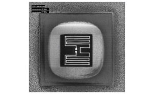
Extract AVR IC Microcontroller embedded firmware from program memory and data memory, crack AVR MCU tamper resistance system can help to readout MCU code;
The same test was applied to a chip with a programmed security fuse. the memory gets fully erased before the security fuse is erased. However some security flaws still could exist. Although nothing could be extracted directly by reading the memory when the fuse is erased, power glitch tricks could work. For example, after seven minutes of exposure to the UV light (253 nm peak, 12 mW/cm2) the memory content can be read non-corrupted at VDD below 2.2 V, but the security fuse remains active up to 4.8 V.
If the attacker works out the exact time when the data from memory is latched into the output shift register and the time when the state of the security fuse is checked, he might be able to extract the memory contents by reducing the power supply down to 2 V for the data latching and increasing it to 5 V to make the security fuse inactive.
Extract AVR MCU Firmware
Extract AVR MCU Firmware from flash and eeprom memory, disable the security fuse bit of AVR microcontroller and unlock microprocessor program memory, read the firmware out from AVR MCU;
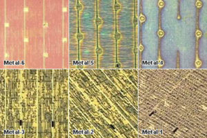
Extract AVR MCU Firmware from flash and eeprom memory, disable the security fuse bit of AVR microcontroller and unlock microprocessor program memory, read the firmware out from it;
The first experiment was performed on the Microchip PIC12C509 microcontroller with UV EPROM. The chip was programmed with all 0’s and exposed to UV light for different periods of time. Then it was read in the test board at different power supply voltages to estimate the threshold level for each EPROM cell in the memory array.
We assumed that the reference voltage is tied to the power supply line and therefore the threshold level of the transistor VTH = K VDD, where K is usually close to 0.5. The fact that we do not measure the exact threshold voltage of the transistor does not affect our results because we are interested in the relative erase timing between the memory and the security fuse.
Extract PLD Chip Eeprom
Extract PLD Chip Eeprom out, the format of the readout file from PLD chip memory will be JED, crack PLD chip protective mechanism to reset the PLD to unlock status;
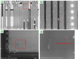
Extract PLD Chip Eeprom out, the format of the readout file from PLD chip memory will be JED, crack PLD chip protective mechanism to reset the PLD to unlock status;
We undertook the evaluation of some microcontrollers with different memory types to investigate the possible influence of data remanence on EPROM, EEPROM and Flash memories. For that purpose we built a special test board controlled by a PC via a parallel interface (Figure 44). The board has two programmable power supplies for generating VDD and VPP voltages, a programming interface with bidirectional voltage level converters, and sockets for microcontroller chips. That allowed us to control the voltages applied to the chip under test with 100 µV precision and apply any signals within a 1 µs time frame.
 Posted in Break IC |
  Tags: extract pld chip binary, extract pld chip data, extract pld chip firmware, extract pld chip flash, extract pld chip heximal, extract pld chip program, extract pld chip software, extract pld chip source code |
  Comments Closed
Extract PLD IC Source Code
Extract PLD IC Source Code from PLD chip memory, crack PLD IC tamper resistance system and disable the security fuse bit, readout the firmware from PLD IC memory;
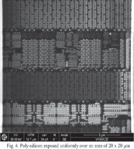
Extract PLD IC Source Code from PLD chip memory, crack PLD IC tamper resistance system and disable the security fuse bit, readout the firmware from PLD IC memory
Obviously, in a floating gate memory cell, the floating gate itself cannot be accessed. Its voltage is controlled through capacitive coupling with the external nodes of the device. Often, the floating-gate transistor is modelled by a capacitor equivalent circuit called the capacitor model. In practice, write/erase characteristics for many EEPROM/Flash memories are close to that of a charge/discharge of a capacitor. Meanwhile there are some differences in how the charge/discharge process takes place in real memory cells. There is an initial delay between the time the voltages are applied to the cell, and the charge starting to be removed or injected.
This delay is caused by the need for very high electric fields to be created inside the floating-gate transistor to start the injection or tunnelling process. Some EEPROM cells have been reported to have nonuniformity during the erase operation. As a result, it might take longer to erase a half-charged cell than a fully-charged cell. In addition, an ideal capacitor discharges exponentially: q = q0 e−t. Applied to the floating gate, that would mean that after t=10 the charge is totally removed from the cell.In practice this doesn’t happen, because the parameters of the cell’s transistor change as the charge is removed from its floating gate. All the above-mentioned problems could seriously affect data remanence in floating-gate memories.
The main difficulty with analysis of the floating-gate memory devices, especially EEPROM and Flash, is the variety of different designs and implementations from many semiconductor manufacturers. There are hundreds of different types of floating-gate transistor, each with its own characteristics and peculiarities. It means that for security applications where data remanence could cause problems, careful testing should be applied to the specific non-volatile memory device used in the system.
Posted in Break IC |
Tags: extract pld ic binary, extract pld ic code, extract pld ic content, extract pld ic data, extract pld ic eeprom, extract pld ic file, extract pld ic firmware, extract pld ic flash, extract pld ic heximal, extract pld ic program |
Comments Closed
Extract PLD IC Firmware
Extract PLD IC Firmware include program of flash memory and data of eeprom memory, PLD IC embedded content can be cloned and copy the code to new PLD chip;
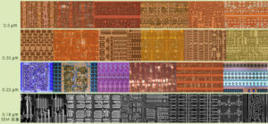
Extract PLD IC Firmware include program of flash memory and data of eeprom memory, PLD IC embedded content can be cloned and copy the code to new PLD chip;
Programmed floating-gate memories cannot store information forever. Various processes (such as field-assisted electron emission and ionic contamination) cause the floating gate to lose the charge, and go faster at higher temperatures. Another failure mode in the very thin tunnel oxides used in Flash memories is programming disturb, where unselected erased cells adjacent to selected cells gain charge when the selected cell is written.
This is not enough to change the cell threshold sufficiently to upset a normal read operation, but could cause problems to the data retention time and should be considered during measurement of the threshold voltage of the cells for data analysis and information recovery. Typical guaranteed data retention time for EPROM, EEPROM and Flash memories are 10, 40 and 100 years respectively.
Posted in Break IC |
Tags: extract pld ic binary, extract pld ic code, extract pld ic content, extract pld ic data, extract pld ic eeprom, extract pld ic file, extract pld ic firmware, extract pld ic flash, extract pld ic heximal, extract pld ic program |
Comments Closed
Extract PLD MCU Code
Extract PLD MCU Code from program memory and data eeprom, cut off the fuse bit embedded inside PLD chip by MCU cracking technique and readout code from PLD.
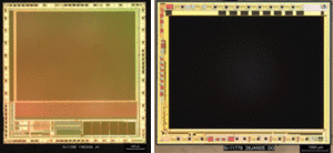
Extract PLD MCU Code from program memory and data eeprom, cut off the fuse bit embedded inside PLD chip by MCU cracking technique and readout code from PLD
The changes in the cell threshold voltage caused by write/erase cycles are particularly apparent in virgin and freshly-programmed cells. It is possible to differentiate between programmed-and-erased and never-programmed cells, especially if the cells have only been programmed and erased once, since virgin cell characteristics will differ from the erased cell characteristics. The changes become less noticeable after ten program/erase cycles.
Extract ARM Chip
Decapsulate ARM MCU package and extract ARM Chip locked memory content from ARM MCU memory needs to get access to databus of ARM MCU by cracking MCU fuse;
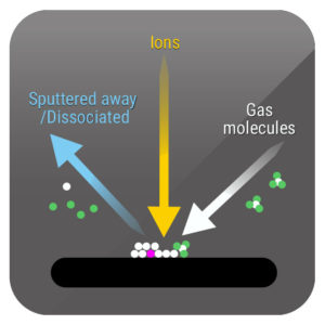
Decapsulate ARM MCU package and extract ARM Chip locked memory content from ARM MCU memory needs to get access to databus of ARM MCU by cracking MCU fuse
Another phenomenon which helps with this is overerasing. If the erase cycle is applied to an already-erased cell, it leaves the floating gate positively charged, thus turning the memory transistor into a depletion-mode transistor. To avoid this problem, some devices, for example Intel’s original ETOX devices, first program all cells to 0’s before erasing them to 1’s. In later devices this problem was solved by redesigning the cell to avoid excessive overerasing, however even with this protection there is still a noticeable threshold shift when a virgin cell is programmed and erased.