 Extract ARM IC Embeded Program
 April 19th, 2013 |
  Author:
 Extract ARM IC Embeded Program from ARM Microcontroller memory, crack ARM microprocessor security fuse bit by focus ion beam and readout the code from MCU;
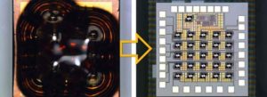
Extract ARM IC Embeded Program from ARM Microcontroller memory, crack ARM microprocessor security fuse bit by focus ion beam and readout the code from MCU
The amount of trapped charge can be detected by measuring the gate-induced drain leakage current of the cell, or its effect can be observed indirectly by measuring the threshold voltage of the cell. In older devices, which had the reference voltage for the sense amplifier tied to the device supply voltage, it was often possible to do this by varying the device supply voltage. In newer devices, it is necessary to change the parameters of the reference cell used in the IC firmware reverse engineering process, either by re-wiring portions of the cell circuitry or by using undocumented test modes built into the device by manufacturers.
 Posted in Break IC |
  Tags: extract arm ic binary, extract arm ic code, extract arm ic content, extract arm ic data, extract arm ic eeprom, extract arm ic file, extract arm ic firmware, extract arm ic flash, extract arm ic heximal, extract arm ic program |
  Comments Closed
Extract ARM MCU IC Chip
Extract ARM MCU IC Chip embedded firmware from program memory and data memory, unlock secured microcontroller by focus ion beam facilities and copy extracted code from open microprocessor;
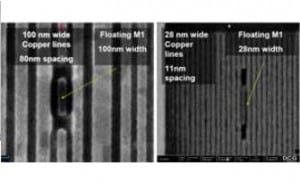
Extract ARM MCU IC Chip embedded firmware from program memory and data memory, unlock secured microcontroller by focus ion beam facilities and copy extracted code from open microprocessor;
There are two basic processes that allow placing the electrons on the floating gate – Fowler-Nordheim tunnelling and channel hot electron (CHE) injection. Both processes are destructive to the very thin dielectric between the floating gate and the channel of a transistor.
As a result, the number of possible cycles is limited because the floating gate slowly accumulates electrons, causing a gradual increase in the storage transistor’s threshold voltage and programming time. After a certain amount of program/erase cycles (typical values were represented in Table 1) it is no longer possible to erase or program the cell. Another negative effect (which is the main restoring failure mode for Flash memory) is negative charge trapping in the gate oxide. It inhibits CHE injection and tunnelling, changes the write and erase times of the cell, and shifts its threshold voltage.
Extract FPGA Chip
Extract FPGA Chip encrypted firmware from secured flash memory and ROM memory, the format will be binary or heximal which can be readout directly by universal programmer after unlock FPGA chip;
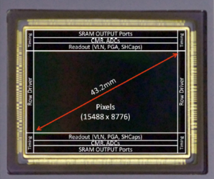
Extract FPGA Chip encrypted firmware from secured flash memory and ROM memory, the format will be binary or heximal which can be readout directly by universal programmer after unlock FPGA chip;
Unlike SRAM which has only two stable logic states, EPROM, EEPROM and Flash cells actually store analog values in the form of a charge on the floating gate of a MOS transistor. The floating-gate charge shifts the threshold voltage of the cell transistor and this is detected with a sense amplifier when the cell is read. The maximum charge the floating gate can accumulate varies from one technology to another and normally is between 103 and 105 electrons. For standard 5 V EEPROM cell, programming causes about a 3.5 V shift in the threshold level. Some modern Flash memory devices employ multiple level detection against IC flash copying, thus increasing the capacity of the memory. There are also memory devices with full analog design which store charge proportional to the input voltage.
Posted in Break IC |
Tags: extract fpga chip binary, extract fpga chip code, extract fpga chip content, extract fpga chip data, extract fpga chip eeprom, extract fpga chip file, extract fpga chip firmware, extract fpga chip flash, extract fpga chip heximal, extract fpga chip program |
Comments Closed
Restore IC Chip Embeded Information
Restore IC Chip Embeded Information from program memory and data memory, the type of IC include MCU, AVR, PLD, CPLD and FPGA chip with the format of heximal which can be readout from Microcontroller memory;
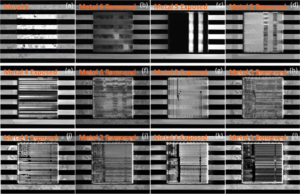
Restore IC Chip Embeded Information from program memory and data memory, the type of IC include MCU, AVR, PLD, CPLD and FPGA chip with the format of heximal which can be readout from Microcontroller memory;
Another important thing to keep in mind is that security information inside PIC18F2550 could be restored even if part of the memory is corrupted. Suppose an attacker has correctly restored only m = 115 bits of an n = 128 bits long secure key, or 90% of the information. Then he will have to search through n!/(m!(n–m)!) = 128!/(115!13!) = 2.12·1017 ~ 258 possible keys. Having 10,000 computers, each performing 1 billion key-search operations per second, the attacker will spend only 6 hours to search through all possible keys.
If only 80% of information or 103 bits of a 128-bit secure key are known, than an attacker will need 2.51·1026 ~ 288 tries. Having even 100 times the capability, the attacker will spend more than a million years searching for the key. So to be sure that symmetric 128-bit keys cannot be retrieved from memory, it should be left without power for the time necessary to corrupt 20% or more of the cells. If error correction for key data is used, this value should be increased correspondingly. In our experiments, we assumed that no error correction was used.
Winbond W79E201 Microcontroller Internal Memory Breaking
Winbond W79E201 Microcontroller Internal Memory Breaking
In order to carry out the Winbond W79E201 Microcontroller Internal Memory Breaking, engineer need to has the general idea about the security system as well as its protection mechanism in this Microcontroller, below we would like to introduce some features of it:
This bit is used to restrict the accessible region of the MOVC instruction. It can prevent the MOVC instruction in external program memory from reading the internal program code.
When this bit is set to logic 0, a MOVC instruction in external program memory space will be able to access code only in the external memory, not in the internal memory.
A MOVC instruction in internal program memory space will always be able to access the ROM data in both internal and external memory. If this bit is logic 1, there are no restrictions on the MOVC instruction.
This bit is used to enable/disable the encryption logic for code protection. Once encryption feature is enabled, the data presented on port 0 will be encoded via encryption logic. Only whole chip erase will reset this bit before Winbond W79E201 Microcontroller Internal Memory Breaking.

ABSOLUTE MAXIMUM RATINGS
Oscillator Control
W79E201 allow user to diminish the gain of on-chip oscillator amplifier by using programmer to set the bit B7 of security register. Once B7 is set to 0, a half of gain will be decreased. Care must be taken if user attempts to diminish the gain of oscillator amplifier, reducing a half of gain may improperly affect the external crystal operation at high frequency above 24 MHz. The value of R and C1,C2 may need some adjustment while running at lower gain.
Restore Winbond W78IE54 MCU Encrypted Heximal
Restore Winbond W78IE54 MCU Encrypted Heximal
As we all know that in the common situation, the status of a MCU W78IE54 will be set as encrypted, and only through disable the security fuse bit can Restore Winbond W78IE54 MCU Encrypted Heximal. hereby we would like to introduce the security system of W78IE54:
During the on-chip MTP-ROM programming mode, the MTP-ROM can be programmed and verified repeatedly. Until the code inside the MTP-ROM is confirmed OK, the code can be protected. The protection of MTP-ROM and those operations on it are described below.
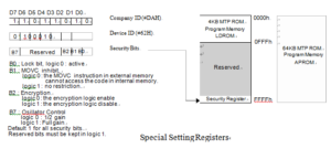
special setting register
The W78IE54 has several Special Setting Registers, including the Security Register and Company/Device ID Registers, which can not be accessed in programming mode before Restore Winbond W78IE54 MCU Encrypted Heximal. Those bits of the Security Registers can not be changed once they have been programmed from high to low.
They can only be reset through erase-all operation. The contents of the Company ID and Device ID registers have been set in factory. The Security Register is located at the 0FFFFH of the LDROM space.
Lock bit
This bit is used to protect the customer’s program code in the W78E62B. It may be set after the programmer finishes the programming and verifies sequence. Once this bit is set to logic 0, both the MTP ROM data and Special Setting Registers can not be accessed again.
Low temperature data remanence in SRAM
Security engineers are interested in the period of time for which an SRAM device will retain data once the power has been removed. The reason for this is as follows. Many products do cryptographic and other security-related computations using secret keys or other variables that the equipment’s operator must not be able to read out or alter. The usual solution is for the secret data to be kept in volatile memory inside a tamper-sensing enclosure. On detection of a tampering event, the volatile memory chips are powered down or even shorted to ground. If the data retention time exceeds the time required by an opponent to open the device and power up the memory, then the protection mechanisms can be defeated.
In the 1980s, it was realised that low temperatures can increase the data retention time of SRAM to many seconds or even minutes. With the devices available at that time, it was found that increased data retention started about −20°C and increased as temperature fell further. Some devices are therefore designed with temperature sensors; any drop below −20°C is treated as a tampering event and results in immediate memory zeroisation. We set out to repeat this work. Our goal was to find whether the memory devices available in the year 2000 exhibit the same behaviour.
Quoted from “Semi-invasive attacks – A new approach to hardware security analysis” writen by Sergei P. Skorobogatov.
Winbond W78IE52 Microcontroller Protected Eeprom Breaking
Winbond W78IE52 Microcontroller Protected Eeprom Breaking
If we can figure out the root of W78IE52 booting it will be easier for us to locate the security fuse and disable it, furthermore it can help us to find the databus of MCU then through microprobing to get the program out. By default, the W78IE52 boots from APROM program after a power on reset. On some occasions, user can force the W78E62B to boot from the LDROM program via following settings.
The possible situation that you need to enter F04KBOOT mode is when the APROM program can not run properly and device can not jump back to LDROM to execute in-system programming function. Then you can use this F04KBOOT mode to force the W78IE52 jumps to LDROM and excutes in-system programming procedure.
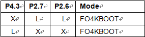
F04KBOOT MODE
When you design your system, you may reserve the pins P2.6, P2.7 to switches or jumpers. For example in a CD-ROM system, you can connect the P2.6 and P2.7 to PLAY and EJECT buttons on the panel. When the APROM program fails to execute the normal application program.
User can press both two buttons at the same time and then turn on the power of the personal computer to force the W78IE52 to enter the F04KBOOT mode. After power on of personal computer, you can release both buttons and finish the in-system programming procedure to update the APROM code from Winbond W78IE52 Microcontroller Protected Eeprom Breaking.
In application system design, user must take care of the P2, P3, ALE, EA and PSEN pin value at reset to prevent from accidentally activating the programming mode or F04KBOOT mode.
Winbond W78ERD2 MCU Locked Program Recovery
After the MCU has been switched to In-System Programming (ISP) Mode, Winbond W78ERD2 MCU Locked Program Recovery can be executed directly, The W78ERD2 equips one 64K byte of main MTP-ROM bank for application program (called APROM) and one 4K byte of auxiliary MTP-ROM bank for loader program (called LDROM).
In the normal operation, the microcontroller executes the code in the APROM. If the content of APROM needs to be modified, the W78ERD2 allows user to activate the In-System Programming (ISP) mode by setting the CHPCON register.
The CHPCON is read-only by default, software must write two specific values 87H, then 59H sequentially to the CHPENR register to enable the CHPCON write attribute. Writing CHPENR register with the values except 87H and 59H will close CHPCON register write attribute.
The W78ERD2 achieves all in-system programming operations including enter/exit ISP Mode, program, erase, read …etc, during device in the idle mode. Setting the bit CHPCON.0 the device will enter in-system programming mode after a wake-up from idle mode from Winbond W78ERD2 MCU Locked Program Recovery.
Because device needs proper time to complete the ISP operations before awaken from idle mode, software may use timer interrupt to control the duration for wake-up from idle mode. This in-system programming feature makes the job easy and efficient in which the application needs to update firmware frequently. In some applications, the in-system programming feature make it possible that the end-user is able to easily update the system firmware by themselves without opening the chassis.
SFRAH,SFRAL:
The objective address of on-chip MTP-ROM in the in-system programming mode. SFRFAH contains the high-order byte of address, SFRFAL contains the low-order byte of address.
SFRFD:
The programming data for on-chip MTP-ROM in programming mode.
SFRCN:
The control byte of on-chip MTP-ROM programming mode.
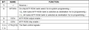
SFRCN (C7)
Data Remanence IC Crack
Data Remanence IC Crack is a method to readout memory content from microcontroller embedded memory which include the program from flash and data from eeprom, the status of MCU can be reset through Focus ion beam tehcnique which is the most commonly used method for Microcontroller unlocking;
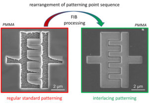
Data Remanence IC Crack is a method to recover memory content from microcontroller embedded memory which include the program from flash and data from eeprom, the status of MCU can be reset through Focus ion beam tehcnique which is the most commonly used method for Microcontroller unlocking
Security processors typically store secret key material in Static RAM, from which power is removed if the device is tampered with. It is widely known that, at temperatures below −20°C, the contents of SRAM can be ‘frozen’; therefore, many devices treat temperatures below this threshold as tampering events. We have done some experiments to establish the temperature dependency of data retention time in modern SRAM devices. Our experiments show that the conventional wisdom no longer holds and that data remanence can be a problem even at higher temperatures.
Data remanence affects not only SRAM but other memory types as well, like DRAM, UV EPROM, EEPROM and Flash. As a result, some information still can be extracted from MCU memory code that has been erased. This could create many problems for secure devices which assume that all the sensitive information is gone once the memory is erased.