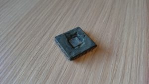
 Restore Microchip PIC18F2550 Memory Data
The OSTS, IOFS and T1RUN bits indicate which clock source is currently providing the device clock. The OSTS bit indicates that the Oscillator Start-up Timer by Restore Microchip PIC18F2550 Memory Data has timed out and the primary clock is providing the device clock in Primary Clock modes.
The IOFS bit indicates when the internal oscillator block has stabi- lized and is providing the device clock in RC Clock modes by Reverse Engineering Encrypted AVR Chip ATtiny261 Software. The T1RUN bit (T1CON<6>) indicates when the Timer1 oscillator is providing the device clock in Secondary Clock modes. In power-managed modes, only one of these three bits will be set at any time. If none of these bits are set, the INTRC is providing the clock or INTOSC has just started and is not yet stable.
The IDLEN bit determines if the device goes into Sleep mode or one of the Idle modes when the SLEEP instruction is executed through Decode Atmel Chip ATtiny461 Encrypted Firmware. The use of the flag and control bits in the OSCCON register is discussed in more detail in Section 3.0 “Power-Managed Modes”.
Note 1: The Timer1 oscillator must be enabled to select the secondary clock source. The Timer1 oscillator is enabled by setting the T1OSCEN bit in the Timer1 Control register (T1CON<3>) in order to Break Encrypted Microprocessor ATtiny861 Embedded Heximal. If the Timer1 oscillator is not enabled, then any attempt to select a secondary clock source will be ignored.
2: It is recommended that the Timer1 oscillator be operating and stable before selecting the secondary clock source or a very long delay may occur while the Timer1 oscillator starts from Restore Microchip PIC18F2550 Memory Data.
PIC18LF2525 devices contain circuitry to prevent clock “glitches” when switching between clock sources. A short pause in the device clock occurs during the clock switch to Crack MCU Program. The length of this pause is the sum of two cycles of the old clock source and three to four cycles of the new clock source for the purpose of Break Atmel MCU ATmega1281 Locked Heximal. This formula assumes that the new clock source is stable. Clock transitions are discussed in greater detail in Section 3.1.2 “Entering Power-Managed Modes”.
