 Read ARM Chip Embeded Firmware
 May 19th, 2013 |
  Author:
 Read ARM Chip Embeded Firmware out needs to modify circuitry pattern, through which the tamper resistance system will be disable through ARM microcontroller cracking, extract arm MCU code from its flash memory;
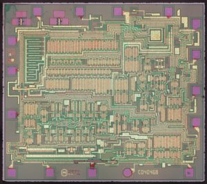
Read ARM Chip Embeded Firmware out needs to modify circuitry pattern, through which the tamper resistance system will be disable through ARM microcontroller cracking, extract arm MCU code from its flash memory
Some microcontrollers have an incorrectly designed security protection fuse, which gets erased earlier than the memory. As a result, if the chip erase operation is terminated prematurely, information could be read from the on-chip memory in a normal way. That was the case, for example, for the Atmel AT89C51 microcontroller. When this became known in the late nineties, Atmel redesigned the chip layout and improved security to prevent this attack, so that chips manufacturers design their products so that the security fuses cannot be erased before the main memory is entirely cleared, thus preventing this low cost attack on their devices.
Read ARM IC Software
Read ARM IC Software from ARM microcontroller embedded memory by extraction, crack ARM MCU protection and cut off the security fuse bit will help to disable the protection over ARM microprocessor;
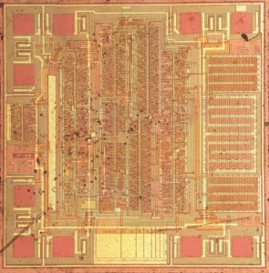
Read ARM IC Software from ARM microcontroller embedded memory by extraction, crack ARM MCU protection and cut off the security fuse bit will help to disable the protection over ARM microprocessor
Even if non-invasive methods do not work, invasive methods could help. For example, the memory control circuit can be modified under a FIB to directly access the reference voltage, the current source or the control gate voltage. Finally, some chips program all the memory locations before applying the erase operation. This makes it almost impossible to extract any useful information from the erased memory. One more thing should be mentioned in connection with hardware security.
 Posted in Break IC |
  Tags: read arm ic binary file, read arm ic embed firmware, read arm ic encrypt eeprom, read arm ic flash program, read arm ic heximal content, read arm ic protect software, read arm ic source code |
  Comments Closed
Read ARM MCU Firmware
Read ARM MCU Firmware out from ARM microprocessor embedded memory, cut off the security fuse bit connected from processor to memory by Microcontroller cracking technique will help, and copy the extracted code to new MCU;
Read ARM MCU Firmware out from ARM microprocessor embedded memory
Fortunately, the extraction from the erased memory technique can only be applied to a very limited number of chips with EEPROM/Flash memory. First, some microcontrollers such as in the Texas Instruments MSP430 family of microcontrollers have an internally stabilized supply voltage for the on-chip memory. Changing the power supply from 1.8 V to 3.6 V does not affect memory read operation from partially erased cells.
Second, most microcontrollers fully reset and discharge the memory control circuit if the chip is reset or the programming mode is re-entered. But still, if the memory contents do not disappear completely, this represents a very serious threat to any security based on an assumption that the information is irrecoverable after one memory erase cycle.
Read FPGA Chip Embeded Firmware
Read FPGA Chip Embeded Firmware from FPGA Processor memory, unlock FPGA Processor secured protection and extract the encrypted code out from chip memory;
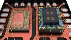
Read FPGA Chip Embeded Firmware from FPGA Processor memory, unlock FPGA Processor secured protection and extract the encrypted code out from chip memory;
In our next test we programmed the chip with all 0’s before applying the erase operation. As a result we were unable to distinguish between previously programmed and non-programmed cells. That means that pre-programming the cells before the erase operation could be a reasonably good solution to increase the security of the on-chip memory.
Read FPGA IC Chip Software Code
Read FPGA IC Chip Software Code from FPGA controller program memory and data memory, decapsulate FPGA processor’s protection and cut off the security fuse bit through MCU cracking invasive method and extract code out from FPGA MCU memory;
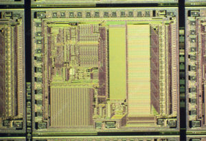
Read FPGA IC Chip Software Code from FPGA controller program memory and data memory, decapsulate FPGA processor’s protection and cut off the security fuse bit through MCU cracking invasive method and extract code out from FPGA MCU memory
At the same time the memory analysis and extraction is complicated by the fact that the difference in threshold voltages between the memory cells is larger than within the cell itself. The practical way to avoid this problem is to use the same cell as a reference and compare the measured threshold level with itself after the extra erase operation is applied to the chip. Very similar results were received for the EEPROM data memory inside the same PIC16F84A chip. The only difference was that the threshold voltage after ten erase cycles was very close to that of the fully erased cell, thus making it almost impossible to recover the information if the erase operation was applied more than ten times.
Read FPGA MCU Microcontroller IC Chip Firmware
Read FPGA MCU Microcontroller IC Chip Firmware is a reverse process of FPGA IC chip manufacturer, the FPGA IC will be cracked and source code can be readout from FPGA chip memory;
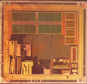
Read FPGA MCU Microcontroller IC Chip Firmware is a reverse process of FPGA IC chip manufacturer, the FPGA IC will be cracked and source code can be readout from FPGA chip memory
Applying the above test to differently programmed and erased chips we were able to build the diagrams for threshold voltage dependence in the Flash program memory from different factors such as the number of erased cycles (Figure 47) and memory address. As can be seen, the charge is not entirely removed from the floating gate even after one hundred erase cycles thus making it possible for the information to be extracted from the memory. This was measured on a sample after 100 program/erase cycles to eliminate the effect of the threshold shift taking place in a virgin cell.
Read DSP Chip Program
Read DSP Chip Program out from program memory and data memory, disable the tamper protection mechanism over the DSP chip by Microcontroller cracking technique, and copy the firmware to new DSP Chip;
Read DSP Chip Program out from program memory and data memory, disable the tamper protection mechanism over the DSP chip by Microcontroller cracking technique, and copy the firmware to new DSP Chip;
To achieve the result another trick was used in addition to the power glitch. The threshold voltage of all the floating gate transistors inside the memory array was shifted temporarily by VW = 0.6–0.9 V, so that VTH = K VDD − VW. As a result it became possible to measure the threshold voltage of an erased cell which is close to 0 V. This was achieved by precisely controlling the memory erase operation, thus allowing the substrate and control gates to be precharged and terminating the process before the tunnelling is started.
As a result, the excess charge is trapped in the substrate below the floating gate, and shifts the threshold of the transistor. The process of recombination of the trapped excess charge could take up to one second, which is enough to read the whole memory from the device. This can be repeated for different supply voltages combined with power glitches, in order to estimate the threshold of all the transistors in the memory array.
Read DSP IC Embeded Source Code
Read DSP IC Embeded Source Code from protective memory which include flash and eeprom ones, crack security fuse bit inside DSP IC chip and extract the firmware from DSP IC memory;
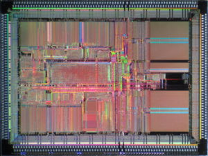
Read DSP IC Embeded Source Code from protective memory which include flash and eeprom ones, crack security fuse bit inside DSP IC chip and extract the firmware from DSP IC memory
We performed an experiment to estimate how much information could be extracted from the PIC16F84A chip after a normal erase operation was applied to it. As can be seen from Figure 46 the memory is completely erased and read as all 1’s well before the end of the standard 10 ms erase cycle. The threshold of the cell’s transistors becomes very low after the erase and cannot be measured the same way as with UV EPROM because the chip stops functioning if the power supply drops below 1.5 V.
With the power glitch technique, it is possible to reduce the supply voltage down to 1 V for a short period of time – enough for the information from memory to be read and latched into the internal buffer. But this is still not enough to shift the reference voltage of the sense amplifier low enough to detect the threshold of the erased cells.
Posted in Break IC |
Tags: read dsp ic binary file, read dsp ic embeded firmware, read dsp ic encrypted eeprom, read dsp ic flash program, read dsp ic heximal content, read dsp ic protected software, read dsp ic source code |
Comments Closed
Read DSP Microcontroller MCU IC Chip Program
Read DSP Microcontroller MCU IC Chip Program out from Microprocessor’s memory, disable the security fuse bit by focus ion beam which is commonly used method for Microcontroller cracking and extract memory content from MCU;
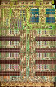
Read DSP Microcontroller MCU IC Chip Program out from Microprocessor’s memory, disable the security fuse bit by focus ion beam which is commonly used method for Microcontroller cracking and extract memory content from MCU
In our early experiments with the security protection in PIC microcontrollers, I noticed that the same PIC16F84 chip behaves differently if it is tested right after the erase operation was completed. As this microcontroller is no longer in use and has been replaced by the PIC16F84A, the testing was applied to the new chip.
Posted in Break IC |
Tags: read microcontroller dsp mcu binary file, read microcontroller dsp mcu embeded firmware, read microcontroller dsp mcu encrypted eeprom, read microcontroller dsp mcu flash program, read microcontroller dsp mcu heximal content, read microcontroller dsp mcu protected software, read microcontroller dsp mcu source code |
Comments Closed
Read CPLD Chip Microcontroller IC JED
Read CPLD Chip Microcontroller IC JED File out from CPLD chip memory, copy JED file to new CPLD chip which can provide the same functions as original one after reset the status of CPLD by Microcontroller unlock skill;
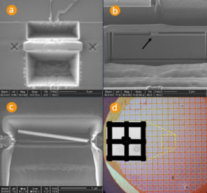
Read CPLD Chip Microcontroller IC JED File out from CPLD chip memory, copy JED file to new CPLD chip which can provide the same functions as original one after reset the status of CPLD by Microcontroller unlock skill
Our next experiment was done to the PIC16F84A microcontroller which has Flash program memory and EEPROM data memory. A similar test sequence was applied with the only difference that electrical erasing was used. A huge difference in the memory behaviour can be observed. The memory erase starts 65 µs after the ‘chip erase’ command was received and by 75 µs the memory is erased.
However, this time changes if the temperature or the supply voltage is changed. For example, if the chip is heated to 35°C the memory erase starts at 60 µs and is finished by 70 µs. The security fuse requires at least 125 µs to be erased giving at least five times excess for reliable memory erase. Reducing the power supply voltage increases the erase time for both the memory and the fuse erase, so that the ratio remains practically the same.
It should be mentioned that unless terminated by the hardware reset, the chip erase operation lasts for at least 1 ms. Both this fact and the fast erase time give an impression that EEPROM and Flash memories have fewer problems with data remanence and therefore should offer better security protection. We decided to investigate whether this is true or not.