Decrypt PIC18F2420 MCU Encrypted Program
 June 27th, 2013 |
  Author:
 Decrypt PIC18F2420 MCU Encrypted Program
Sampled BOD in Active mode will cause noise when bandgap is used as reference
Bandgap measurement with the ADC is non-functional when VCC is below 2.7V otherwise the procedures of Decrypt PIC18F2420 MCU encrypted Program will be paused.
BOD will be enabled after any reset
Writing EEPROM or locked while unlocking any of them will not work
ADC has increased INL error for some operating conditions
DAC has increased INL or noise for some operating conditions
VCC voltage scaler for AC is non-linear
Maximum operating frequency below 1.76V is 8 MHz
Bandgap voltage input for the ACs cannot be changed when used for both ACs simultaneously
If the bandgap voltage is selected as input for one Analog Comparator (AC) and then selected/deselected as input for the another AC, the first comparator will be affected for up to 1 us and could potentially give a wrong comparison result after the locked of chip being unlocked.
Problem fix/Workaround
If the Bandgap is required for both ACs simultaneously, configure the input selection for both ACs before enabling any of them.
ADC gain stage output range is limited to 2.4 V
The amplified output of the ADC gain stage will never go above 2.4 V, hence the differential input will only give correct output when below 2.4 V/gain. For the available gain settings, this gives a differential input range of:
Problem fix/Workaround
Keep the amplified voltage output from the ADC gain stage below 2.4 V in order to get a correct result, or keep ADC voltage reference below 2.4 V.
Sampled BOD in Active mode will cause noise when bandgap is used as reference
Using the BOD in sampled mode when the device is running in Active or Idle mode will add noise on the bandgap reference for ADC, DAC and Analog Comparator after the chip’s locked can be unlocked.
Problem fix/Workaround
If the bandgap is used as reference for either the ADC, DAC and Analog Comparator, the BOD must not be set in sampled mode.
Bandgap measurement with the ADC is non-functional when VCC is below 2.7V
The ADC cannot be used to do bandgap measurements when VCC is below 2.7V.
Problem fix/Workaround
If internal voltages must be measured when VCC is below 2.7V, measure the internal 1.00V reference instead of the bandgap.
BOD will be enabled after any reset from Decrypt PIC18F2420 MCU encrypted Program
If any reset source goes active, the BOD will be enabled and keep the device in reset if the VCC voltage is below the programmed BOD level. During Power-On Reset, reset will not be released until VCC is above the programmed BOD level even if the BOD is disabled before unlock chip data.
Problem fix/Workaround
Do not set the BOD level higher than VCC even if the BOD is not used.
 Posted in
Readout DSP Chip TMS320LF2406APZAR Program
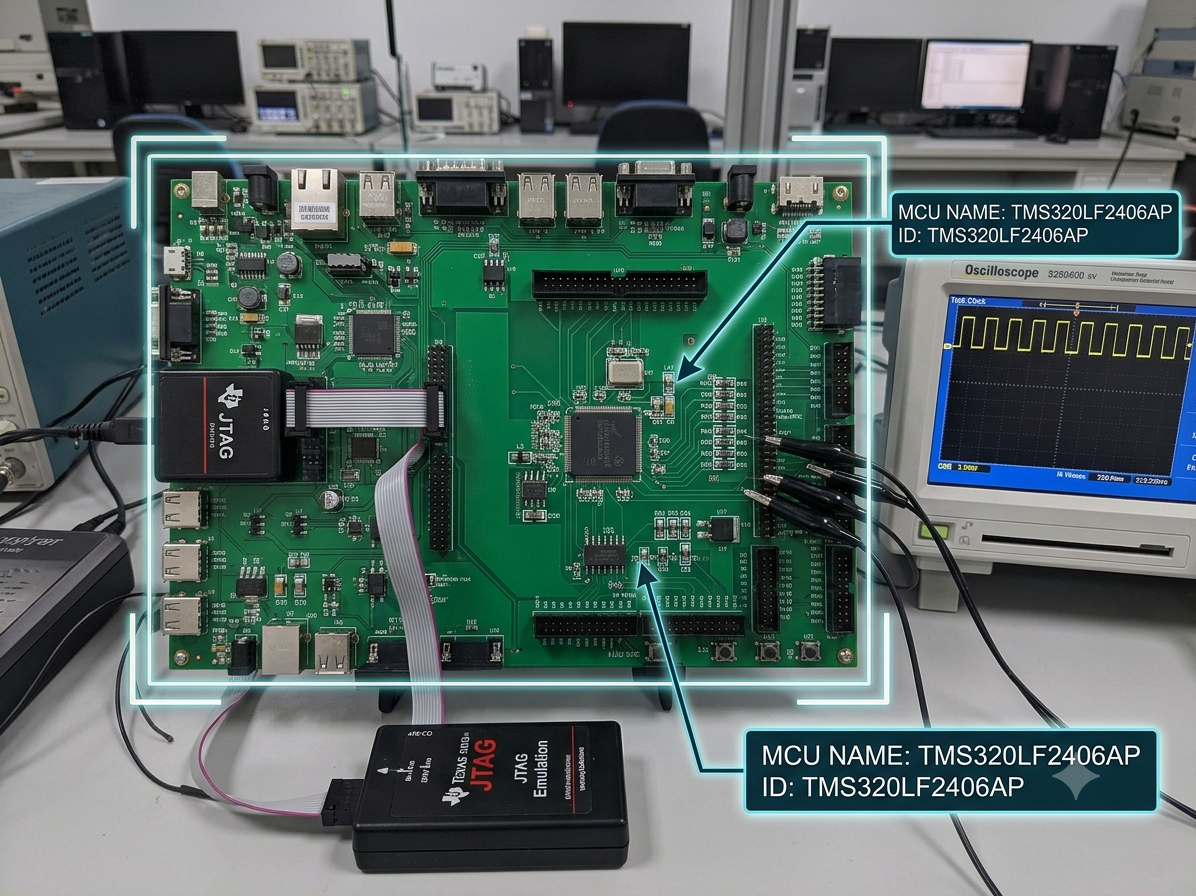
The tms320lf2406apzar is a high-performance dsp device from texas instrument that has been widely used in industrial and commercial control applications requiring fast signal processing, accurate real-time calculation, and reliable embedded operation. As a specialized microprocessor platform, this chip provides strong processing capability for applications such as motor control systems, industrial automation equipment, power conversion devices, robotics, medical instruments, communication systems, and intelligent measurement platforms.
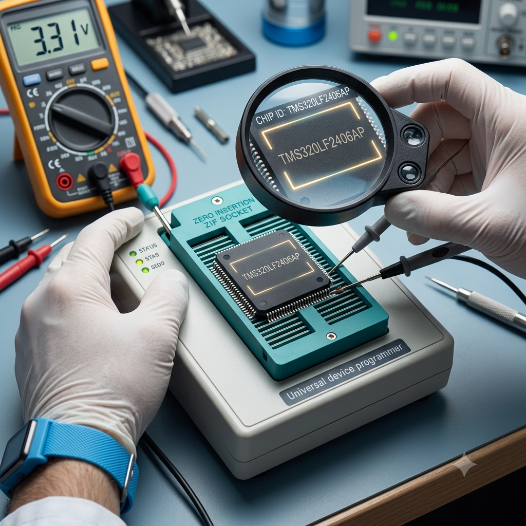
Unlike conventional microcontroller solutions, this dsp architecture is optimized for mathematical operations, digital signal processing, and complex control algorithms. During product development, manufacturers store essential firmware, control program logic, calibration data, and configuration information inside internal memory, including flash and other non-volatile storage areas. Over time, many organizations face challenges when original development documents, software projects, or engineering archive files are unavailable. Additionally, stored resources may be configured with protective, protected, locked, secured, or encrypted mechanisms, making access to original binary, heximal, and source code resources difficult without professional analysis.
High-Performance Static CMOS Technology
− 25-ns Instruction Cycle Time (40 MHz)
− 40-MIPS Performance
− Low-Power 3.3-V Design
D Based on TMS320C2xx DSP CPU Core
− Code-Compatible With F243/F241/C242
− Instruction Set and Module Compatible
With F240
D Flash (LF) and ROM (LC) Device Options
− LF240xA: LF2407A, LF2406A,
LF2403A, LF2402A
− LC240xA: LC2406A, LC2404A,
LC2403A, LC2402A
D On-Chip Memory
− Up to 32K Words x 16 Bits of Flash
EEPROM (4 Sectors) or ROM
− Programmable “Code-Security” Feature for the On-Chip Flash/ROM
− Up to 2.5K Words x 16 Bits of
Data/Program RAM
− 544 Words of Dual-Access RAM
− Up to 2K Words of Single-Access RAM
D Boot ROM (LF240xA Devices)
− SCI/SPI Bootloader
D Up to Two Event-Manager (EV) Modules (EVA and EVB), Each Includes:
− Two 16-Bit General-Purpose Timers
− Eight 16-Bit Pulse-Width Modulation (PWM) Channels Which Enable:
− Three-Phase Inverter Control
− Center- or Edge-Alignment of PWM Channels
− Emergency PWM Channel Shutdown With External PDPINTx Pin
− Programmable Deadband (Deadtime) Prevents Shoot-Through Faults
− Three Capture Units for Time-Stamping of External Events
− Input Qualifier for Select Pins
− On-Chip Position Encoder Interface Circuitry
− Synchronized A-to-D Conversion
− Designed for AC Induction, BLDC,
Switched Reluctance, and Stepper Motor Control
− Applicable for Multiple Motor and/or Converter Control
D External Memory Interface (LF2407A)
− 192K Words x 16 Bits of Total Memory:
64K Program, 64K Data, 64K I/O
D Watchdog (WD) Timer Module
D 10-Bit Analog-to-Digital Converter (ADC)
− 8 or 16 Multiplexed Input Channels
− 500-ns MIN Conversion Time
− Selectable Twin 8-State Sequencers
Triggered by Two Event Managers
D Controller Area Network (CAN) 2.0B Module (LF2407A, 2406A, 2403A)
D Serial Communications Interface (SCI)
D 16-Bit Serial Peripheral Interface (SPI)
(LF2407A, 2406A, LC2404A, 2403A)
D Phase-Locked-Loop (PLL)-Based Clock Generation
D Up to 40 Individually Programmable,
Multiplexed General-Purpose Input / Output (GPIO) Pins
D Up to Five External Interrupts (Power Drive Protection, Reset, Two Maskable Interrupts)
D Power Management:
− Three Power-Down Modes
− Ability to Power Down Each Peripheral Independently
D Real-Time JTAG-Compliant Scan-Based Emulation, IEEE Standard 1149.1† (JTAG)
D Development Tools Include:
− Texas Instruments (TI) ANSI C Compiler,
Assembler/ Linker, and Code Composer
Studio Debugger
− Evaluation Modules
− Scan-Based Self-Emulation (XDS510)
− Broad Third-Party Digital Motor Control Support D Package Options
Our “readout dsp chip tms320lf2406apzar program” service provides specialized support for authorized recovery, preservation, and analysis of valuable embedded software assets stored inside this advanced dsp platform. Through comprehensive semiconductor evaluation and firmware analysis methods, our engineers can examine the internal structure of the microprocessor, identify stored program resources, and assist in recovering available firmware, data, and memory information. Depending on the device condition and project requirements, advanced laboratory procedures, including controlled decapsulate analysis, may be used to gain deeper understanding of internal storage structures.
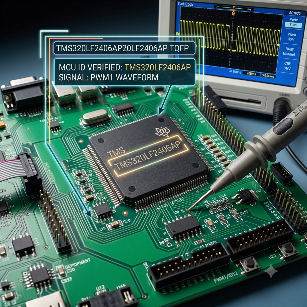
By combining hardware investigation with software interpretation, our team can retrieve available binary images, organize heximal information, and reconstruct meaningful file and archive records. Professional decode processes help transform collected information into structured engineering resources, allowing customers to analyze original firmware behavior and preserve important technical knowledge. For projects involving locked, secured, or encrypted devices, our specialists evaluate the architecture of the target texas instrument dsp and determine suitable recovery approaches. Rather than simply attempting to attack, break, or hack a device, the objective is to preserve customer-owned technology and support engineering continuity. Recovered resources may assist with product maintenance, compatibility studies, controlled clone development, and duplicate validation for legacy systems.
The recovery and analysis workflow for the tms320lf2406apzar requires a combination of dsp expertise, embedded software knowledge, and semiconductor understanding. Engineers first evaluate the condition of the chip, study the relationship between hardware operation and stored memory content, and identify the organization of available flash, firmware, and configuration regions. Extracted binary and heximal information is carefully analyzed to reconstruct meaningful program structures and support the creation of updated engineering documentation.
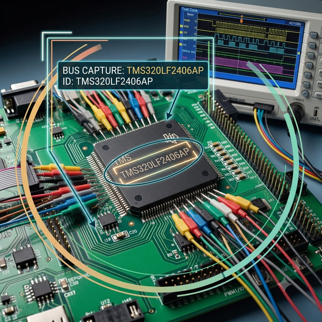
Advanced tools are used to decode recovered data, compare firmware behavior, and identify relationships between application logic and hardware functions. When authorized and technically appropriate, specialized inspection techniques, including selective decapsulate procedures, can provide additional visibility into internal structures of the mcu and microcontroller environments. This process allows engineers to recover valuable information from aging electronic systems where original software files, development environments, or source documentation may no longer exist. The final recovered archive, firmware resources, and technical records provide practical support for redesign, troubleshooting, modernization, and long-term product lifecycle management.
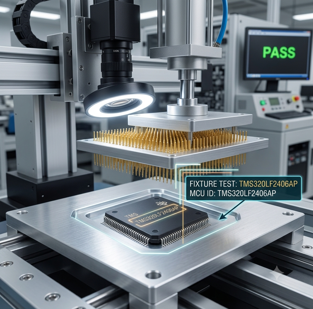
For manufacturers, engineering companies, and maintenance providers, recovering the tms320lf2406apzar program delivers significant advantages in preserving existing investments. Access to historical firmware, validated binary resources, reconstructed source code references, and organized data archives helps reduce redevelopment costs and extend the operational life of proven products.
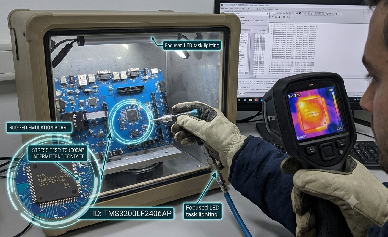
Companies can maintain legacy control systems, support discontinued equipment, migrate designs to updated platforms, and improve technical documentation without starting development again from zero. With professional experience in dsp, texas instrument, microprocessor, and embedded microcontroller analysis, our service provides a reliable pathway for recovering valuable engineering assets and transforming inaccessible chip information into practical resources for future innovation and system continuity.
Crack PIC16F716 MCU Source Code
Crack PIC16F716 MCU Source Code
Crack PIC16F716 MCU Source Code means the source code will be readout from its memory after the PIC16F716 protection has been disabled:
Microcontroller Core Features:
· High-performance RISC CPU
· Only 35 single-word instructions to learn
– All single-cycle instructions except for program branches which are two-cycle
· Operating speed: DC – 20 MHz clock input DC – 200 ns instruction cycle
· Interrupt capability (up to 7 internal/external interrupt sources)
· 8-level deep hardware stack
· Direct, Indirect and Relative Addressing modes
Special Microcontroller Features:
· Power-on Reset (POR)
· Power-up Timer (PWRT) and
Oscillator Start-up Timer (OST)
· Watchdog Timer (WDT) with its own on-chip RC oscillator for reliable operation
· Dual level Brown-out Reset circuitry
– 2.5 VBOR (Typical)
– 4.0 VBOR (Typical)
· Programmable code protection
· Power-Saving Sleep mode
· Selectable oscillator options
· Fully static design
· In-Circuit Serial Programming (ICSP™) CMOS Technology:

Crack PIC16F716 MCU Source Code
· Wide operating voltage range:
– Industrial: 2.0V to 5.5V
– Extended: 3.0V to 5.5V
· High Sink/Source Current 25/25 mA
· Wide temperature range:
– Industrial: -40°C to 85°C
– Extended: -40°C to 125°C
Low-Power Features:
· Standby Current:
– 100 nA @ 2.0V, typical
· Operating Current:
– 14 ìA @ 32 kHz, 2.0V, typical
– 120 ìA @ 1 MHz, 2.0V, typical
· Watchdog Timer Circuit:
– 1 ìA @ 2.0V, typical
· Timer1 Oscillator Current:
– 3.0 ìA @ 32 kHz, 2.0V, typical
Peripheral Features:
· Timer0: 8-bit timer/counter with 8-bit prescaler
· Timer1: 16-bit timer/counter with prescaler can be incremented during Sleep via external crystal/clock
· Timer2: 8-bit timer/counter with 8-bit period register, prescaler and postscaler
· Enhanced Capture, Compare, PWM module:
– Capture is 16-bit, max. resolution is 12.5 ns
– Compare is 16-bit, max. resolution is 200 ns
– PWM maximum resolution is 10-bit
– Enhanced PWM:
– Single, Half-Bridge and Full-Bridge modes
– Digitally programmable dead-band delay
– Auto-shutdown/restart
· 8-bit multi-channel Analog-to-Digital Converter
· 13 I/O pins with individual direction control
· Programmable weak pull-ups on PORTB
Microchip PIC18F2520 Embedded Firmware Extraction
Microchip PIC18F2520 Embedded Firmware Extraction
Microchip PIC18F2520 Embedded Firmware Extraction needs not only know the memory structure, but also the oscillator structure since it is also important for the power glitch method:
Flexible Oscillator Structure:
· Four Crystal modes, up to 40 MHz
· 4x Phase Lock Loop (PLL) – Available for Crystal and Internal Oscillators
· Two External RC modes, up to 4 MHz
· Two External Clock modes, up to 40 MHz
· Internal Oscillator Block:
– Fast wake from Sleep and Idle, 1 ìs typical
– 8 use-selectable frequencies, from 31 kHz to 8 MHz
– Provides a complete range of clock speeds from 31 kHz to 32 MHz when used with PLL
– User-tunable to compensate for frequency drift
· Secondary Oscillator using Timer1 @ 32 kHz
· Fail-Safe Clock Monitor:
– Allows for safe shutdown if peripheral clock stops
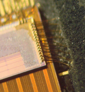
Microchip PIC18F2520 Embedded Firmware Extraction
Converter module:
– Auto-acquisition capability
– Conversion available during Sleep
· Dual Analog Comparators with Input Multiplexing
· Programmable 16-Level High/Low-Voltage
Detection (HLVD) module:
– Supports interrupt on High/Low-Voltage Detection
Special Microcontroller Features:
· C Compiler Optimized Architecture:
– Optional extended instruction set designed to
optimize re-entrant code
· 100,000 Erase/Write Cycle Enhanced Flash
Program Memory Typical
· 1,000,000 Erase/Write Cycle Data EEPROM
Memory Typical
· Flash/Data EEPROM Retention: 100 Years Typical
· Self-Programmable under Software Control
High-Current Sink/Source 25 mA/25 mA
Three Programmable External Interrupts
Four Input Change Interrupts
Up to 2 Capture/Compare/PWM (CCP) modules,
· Priority Levels for Interrupts
· 8 x 8 Single-Cycle Hardware Multiplier
· Extended Watchdog Timer (WDT):
– Programmable period from 4 ms to 131s
one with Auto-Shutdown (28-pin devices)
· Enhanced Capture/Compare/PWM (ECCP)
module (40/44-pin devices only):
– One, two or four PWM outputs
– Selectable polarity
– Programmable dead time
– Auto-shutdown and auto-restart
Copy Lattice CPLD Encrypted File
Copy Lattice CPLD Encrypted File from embedded memory, disable the security fuse by Microcontroller cracking skill and extract the firmware from CPLD chip;
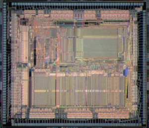
Copy Lattice CPLD Encrypted File from embedded memory, disable the security fuse by Microcontroller cracking skill and extract the firmware from CPLD chip;
Normally a microscope objective has at least two parameters printed on it – magnification and numerical aperture (NA). Modern optical microscopes provide magnification up to 9,000× and 500× magnification is provided by most modern microscopes. Numerical aperture determines the resolving power of an objective, but the total resolution of a microscope system is also dependent upon the numerical aperture of projection optics.
The higher the numerical aperture of the total system the better the resolution. The numerical aperture is related to the angle µ which is one-half of the angular aperture at which the light cone comes to the specimen surface: NA = n sin(µ). The relationship between the numerical aperture and the resolution can used for observation.
 Tags:
Tags:
Copy DSP CPLD Embeded Firmware
Copy DSP CPLD Embeded Firmware from CPLD memory needs to reverse engineering CPLD and get the CPLD scheme in order to locate the security fuse bit of CPLD, and then use Microcontroller cracking technique to remove the protection;
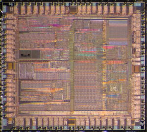
Copy DSP CPLD Embeded Firmware from CPLD memory needs to reverse engineering CPLD and get the CPLD scheme in order to locate the security fuse bit of CPLD, and then use Microcontroller cracking technique to remove the protection;
The most important tool for reverse engineering silicon chips down to 0.18 µm feature size is an optical microscope with a CCD camera to produce mosaics of high-resolution photographs of the chip surface. Not every microscope would do. As light cannot pass through the chip, the microscope should have reflected light illumination. The image should be sharp and without geometric distortion and colour aberration, otherwise it will not be possible to stick all the images together.
The most important parameters of the microscope are resolution and magnification. The resolution of a microscope mainly depends upon its objective lenses and is defined as the smallest distance between two points on a specimen that can still be distinguished as two separate entities. Resolution is a somewhat subjective value in microscopy because at high magnification an image may appear non-sharp but still be resolved to the maximum ability of the objective.
Microchip MCU PIC16F870 Heximal Code Restoration
Microchip MCU PIC16F870 Heximal Code Restoration
The content from original PIC16F870 can be re-attained through Microchip MCU PIC16F870 Heximal Code Restoration procedures:
Microcontroller Core Features:
· High performance RISC CPU
· Only 35 single word instructions to learn
· All single cycle instructions except for program branches which are two-cycle
· Operating speed: DC – 20 MHz clock input DC – 200 ns instruction cycle
· 2K x 14 words of FLASH Program Memory
128 x 8 bytes of Data Memory (RAM) 64 x 8 bytes of EEPROM Data Memory
· Pinout compatible to the PIC16CXXX 28 and 40-pin devices
· Interrupt capability (up to 11 sources)
· Eight level deep hardware stack
· Direct, Indirect and Relative Addressing modes
· Power-on Reset (POR)
· Power-up Timer (PWRT) and Oscillator Start-up Timer (OST)
· Watchdog Timer (WDT) with its own on-chip RC oscillator for reliable operation
· Programmable code protection
· Power saving SLEEP mode
· Selectable oscillator options
· Low power, high speed CMOS FLASH/EEPROM technology
· Fully static design
· In-Circuit Serial Programmingä (ICSPä) via two pins
· Single 5V In-Circuit Serial Programming capability
· In-Circuit Debugging via two pins
· Processor read/write access to program memory
· Wide operating voltage range: 2.0V to 5.5V
· High Sink/Source Current: 25 mA
· Commercial and Industrial temperature ranges
· Low power consumption:
– < 1.6 mA typical @ 5V, 4 MHz
– 20 mA typical @ 3V, 32 kHz
– < 1 mA typical standby current
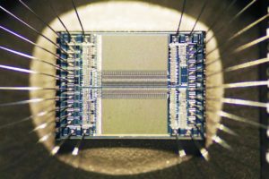
Microchip MCU PIC16F870 Heximal Code Restoration
Peripheral Features:
· Timer0: 8-bit timer/counter with 8-bit prescaler
· Timer1: 16-bit timer/counter with prescaler, can be incremented during SLEEP via external crystal/clock
· Timer2: 8-bit timer/counter with 8-bit period register, prescaler and postscaler
· One Capture, Compare, PWM module
– Capture is 16-bit, max. resolution is 12.5 ns
– Compare is 16-bit, max. resolution is 200 ns
– PWM max. resolution is 10-bit
· 10-bit multi-channel Analog-to-Digital converter
· Universal Synchronous Asynchronous Receiver
Transmitter (USART/SCI) with 9-bit address detection
· Parallel Slave Port (PSP) 8-bits wide, with external RD, WR and CS controls (40/44-pin only)
· Brown-out detection circuitry for Brown-out Reset (BOR)
Recover Freescale MCU MC9S12XDG128 Memory Program
Recover Freescale MCU MC9S12XDG128 Memory Program
The MC9S12XD family will retain the low cost, power consumption, EMC and code-size efficiency advantages currently enjoyed by users of Freescale’s existing 16-Bit MC9S12 MCU Family.
Based around an enhanced S12 core, the MC9S12XD family will deliver 2 to 5 times the performance of a 25-MHz S12 whilst retaining a high degree of pin and code compatibility with the S12 which makes the Recover Freescale MCU MC9S12XDG128 Memory Program becomes more value effectively.
The MC9S12XD family introduces the performance boosting XGATE module. Using enhanced DMA functionality, this parallel processing module offloads the CPU by providing high-speed data processing and transfer between peripheral modules, RAM, Flash EEPROM and I/O ports. Providing up to 80 MIPS of performance additional to the CPU, the XGATE can access all peripherals, Flash EEPROM and the RAM block.
The MC9S12XD family is composed of standard on-chip peripherals including up to 512 Kbytes of Flash EEPROM, 32 Kbytes of RAM, 4 Kbytes of EEPROM, six asynchronous serial communications interfaces (SCI), three serial peripheral interfaces (SPI), an 8-channel IC/OC enhanced capture timer, an 8-channel, 10-bit analog-to-digital converter, a 16-channel, 10-bit analog-to-digital converter, an 8-channel pulse-width modulator (PWM), five CAN 2.0 A, B software compatible modules (MSCAN12), two inter-IC bus blocks, and a periodic interrupt timer. The MC9S12XD family has full 16-bit data paths throughout.
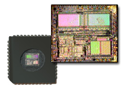
Recover Freescale MCU MC9S12XDG128 Memory Program
The non-multiplexed expanded bus interface available on the 144-pin versions allows an easy interface to external memories The inclusion of a PLL circuit allows power consumption and performance to be adjusted to suit operational requirements from Recover Freescale MCU MC9S12XDG128 Memory Program. System power consumption can be further improved with the new “fast exit from stop mode” feature.
In addition to the I/O ports available in each module, up to 25 further I/O ports are available with interrupt capability allowing wake-up from stop or wait mode.
Family members in 144-pin LQFP will be available with external bus interface and parts in 112-pin LQFP or 80-pin QFP package without external bus interface. See Appendix E Derivative Differences for package options.
Reverse Engineering Microchip PIC16F1913 Memory
Reverse Engineering Microchip PIC16F1913 Memory
Reverse Engineering Microchip PIC16F1913 Memory means delayer the silicon, plastic and metal layer from PIC16F1913 and counter sequence of microcontroller manufacturing:
High-Performance RISC CPU:
· Only 35 instructions to learn:
– All single-cycle instructions except branches
· Operating speed:
– DC – 20 MHz oscillator/clock input
– DC – 200 ns instruction cycle
· Program Memory Read (PMR) capability
· Interrupt capability
· 8-level deep hardware stack
· Direct, Indirect and Relative Addressing modes
Special Microcontroller Features:
· Precision Internal Oscillator:
– Factory calibrated to ±1%, typical
– Software selectable frequency range of
8 MHz to 125 kHz
– Software tunable
– Two-Speed Start-up mode
– External Oscillator fail detect for critical applications
– Clock mode switching during operation for power savings
· Software selectable 31 kHz internal oscillator
· Power-Saving Sleep mode
· Wide operating voltage range (2.0V-5.5V)
· Industrial and Extended temperature range
· Power-on Reset (POR)
· Power-up Timer (PWRT) and Oscillator Start-up
Timer (OST)
· Brown-out Reset (BOR) with software control option
· Enhanced Low-Current Watchdog Timer (WDT) with on-chip oscillator (software selectable nominal 268 seconds with full prescaler) with software enable
· Multiplexed Master Clear with pull-up/input pin
· Programmable code protection
· High-Endurance Flash/EEPROM cell:
– 100,000 write Flash endurance
– 1,000,000 write EEPROM endurance
– Flash/Data EEPROM retention: > 40 years
Low-Power Features:
· Standby Current:
– <100 nA @ 2.0V, typical
· Operating Current:
– 11 ìA @ 32 kHz, 2.0V, typical
– 220 ìA @ 4 MHz, 2.0V, typical
· Watchdog Timer Current:
– 1 ìA @ 2.0V, typical
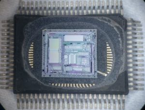
Reverse Engineering Microchip PIC16F1913 Memory
Peripheral Features:
· Liquid Crystal Display module:
– Up to 60/96/168 pixel drive capability on 28/40/64-pin devices, respectively
– Four commons
· Up to 24/35/53 I/O pins and 1 input-only pin:
– High-current source/sink for direct LED drive
– Interrupt-on-change pin
– Individually programmable weak pull-ups
· In-Circuit Serial Programming™ (ICSP™) via two pins if Reverse Engineering Microchip PIC16F1913 Memory
· Analog comparator module with:
– Two analog comparators
– Programmable on-chip voltage reference (CVREF) module (% of VDD)
– Comparator inputs and outputs externally accessible
· A/D Converter:
– 10-bit resolution and up to 8 channels
· Timer0: 8-bit timer/counter with 8-bit programmable prescaler
· Enhanced Timer1:
– 16-bit timer/counter with prescaler
– External Timer1 Gate (count enable)
– Option to use OSC1 and OSC2 as Timer1 oscillator if INTOSCIO or LP mode is selected
· Timer2: 8-bit timer/counter with 8-bit period register, prescaler and postscaler
· Addressable Universal Synchronous
Asynchronous Receiver Transmitter (AUSART)
· Up to 2 Capture, Compare, PWM modules:
– 16-bit Capture, max. resolution 12.5 ns
– 16-bit Compare, max. resolution 200 ns
– 10-bit PWM, max. frequency 20 kHz
· Synchronous Serial Port (SSP) with I2C™
Extract Lattice CPLD Source Code
Lattice CPLD devices have been used extensively in electronic products that require deterministic logic processing, compact implementation, reliable timing, and flexible hardware control. Depending on the specific Lattice family, a cpld can perform functions such as interface conversion, address decoding, signal conditioning, timing generation, peripheral control, and system-level glue logic. These capabilities make programmable logic valuable in industrial automation, telecommunications equipment, instrumentation, medical electronics, transportation systems, consumer products, and specialized control platforms.
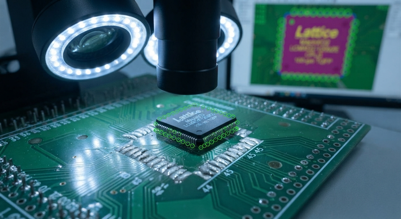
Unlike a conventional microcontroller, a cpld implements hardware logic rather than relying primarily on sequential software execution. Consequently, important design information may exist as embedded configuration data rather than conventional source code. When original development projects, programming files, or engineering archive records have disappeared, recovering the design intent from an existing board can become extremely valuable. Our “lattice cpld source code extraction” service is intended to support authorized customers who need to preserve, document, analyze, or reconstruct legacy programmable-logic designs.
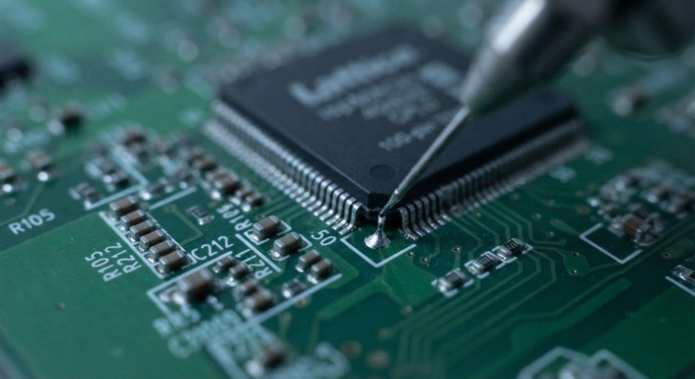
Our engineering process begins by examining the target cpld, its surrounding circuitry, available documentation, and the condition of the original hardware. The objective is to retrieve as much useful engineering information as technically feasible and transform it into practical documentation. Depending on the device family and project requirements, specialists may analyze available configuration data, programming files, binary or heximal representations, pin relationships, timing behavior, and external circuit connections. Where appropriate and authorized, advanced semiconductor analysis and carefully controlled decapsulate examination can provide additional information about internal structures.
Engineers then decode and interpret recovered information to understand implemented logic and reconstruct useful design records. Customers may describe this work using terms such as attack, break, or hack, particularly when the original device is protected, locked, secured, or subject to protective configuration. In professional engineering practice, however, the emphasis is on authorized recovery and preservation. Depending on the technology involved, the recovered result may not be literal original source code; instead, it may consist of configuration information, reconstructed logic descriptions, netlists, behavioral documentation, or other engineering file formats. These resources can subsequently support controlled clone evaluation, duplicate development, redesign, or product maintenance.
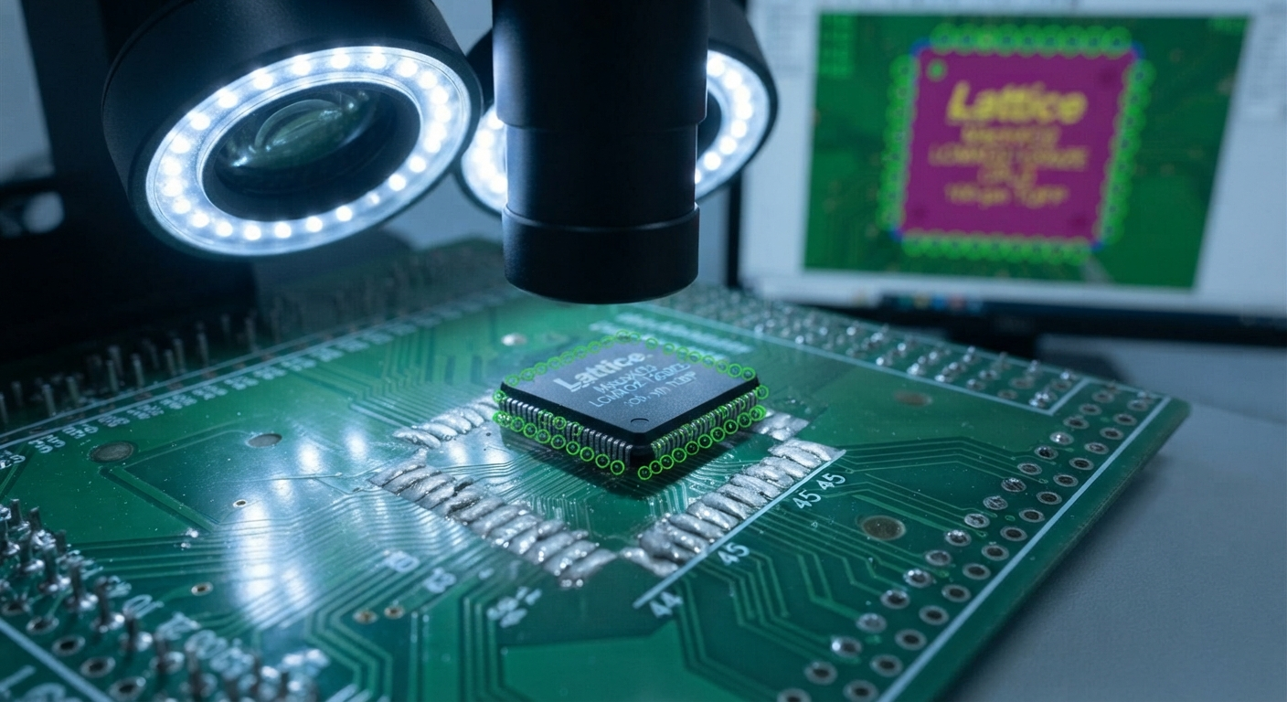
Extract Lattice CPLD Source Code from embedded memory needs to reset the status of CPLD chip from locked to open one by CPLD chip unlocking technique, the content inside the CPLD memory can be readout directly with universal programmer;
A slightly different approach is required for reverse engineering CPLDs and FPGAs. Even if the security protection is defeated and the attacker manages to extract the configuration bitstream file from the device, he will have to spend a substantial amount of time and effort to convert it into the logic equations and primitive blocks for further simulation and analysis. Meantime, there are some companies on the market, for example Bottom Line Technologies [111], which provide bitstream reverse engineering for CPLDs and FPGAs.
A major advantage of reverse engineering programmable logic is the ability to recover design knowledge even when conventional documentation is incomplete. Engineers can correlate the recovered firmware or configuration information with the physical PCB, schematic relationships, signal paths, and system behavior. Although flash, eeprom, and other memory technologies are more commonly associated with stored software, programmable-logic devices can contain their own configuration structures and therefore require a different analytical approach.
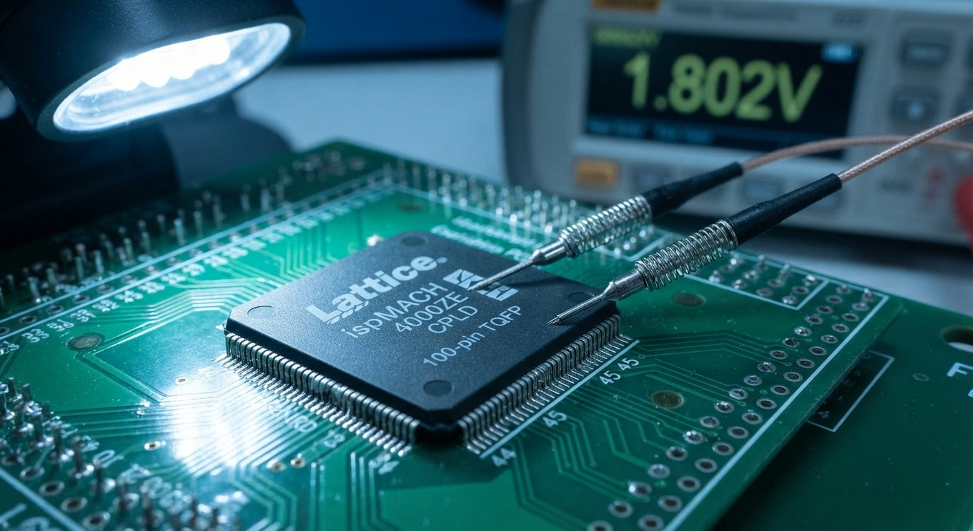
Where a design incorporates an additional microcontroller or processor, its program and firmware can also be considered as part of the overall system investigation. For encrypted, protected, or otherwise inaccessible devices, feasibility depends heavily on the exact Lattice architecture and available evidence. Our specialists therefore evaluate each project individually instead of assuming that every source code extraction will produce an identical result. The final engineering package can include recovered configuration information, reconstructed logic documentation, pin mappings, functional observations, and organized archive materials.
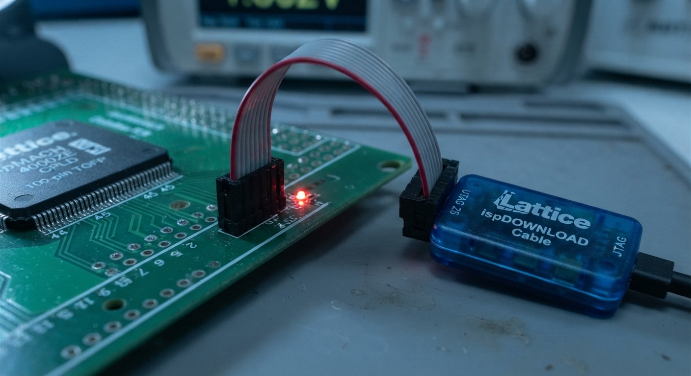
For equipment manufacturers, maintenance organizations, and engineering teams, lattice CPLD recovery can provide substantial lifecycle benefits. Recovering valuable design information can reduce the need to redesign a proven control function from the beginning, particularly when the original designer, development environment, or programming file is no longer available.
The resulting documentation can help engineers repair obsolete equipment, manufacture authorized replacement boards, migrate legacy logic to a newer cpld, verify functional compatibility, and preserve important intellectual property. It can also provide a foundation for future modifications without sacrificing the behavior of an established product. By combining programmable-logic expertise, hardware investigation, configuration-data analysis, and disciplined documentation, our service helps customers convert an existing embedded cpld implementation into practical engineering knowledge for maintenance, reproduction, modernization, and long-term product support.