Archive for the ‘Break IC’ Category
 Break IC ATtiny45 Heximal
 August 3rd, 2010 |
  Author:
 Break IC ATtiny45 and readout Heximal from mcu attiny45 flash memory, unlock microcontroller attiny45 security fuse bit and remove the protection;
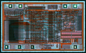
Port B is a 6-bit bi-directional I/O port with internal pull-up resistors (selected for each bit). The Port B output buffers have symmetrical drive characteristics with both high sink and source capability. As inputs, Port B pins that are externally pulled low will source current if the pull-up resistors are activated.
The Port B pins are tri-stated when a reset condition becomes active, even if the clock is not running. Reset input. A low level on this pin for longer than the minimum pulse length will generate a reset, even if the clock is not running.
The minimum pulse length is given in Table 23-3 on page 170. Shorter pulses are not guaranteed to generate a reset. For compatibility with future devices, reserved bits should be written to zero if accessed. Reserved I/O memory addresses should never be written. I/O Registers within the address range 0x00 – 0x1F are directly bit-accessible using the SBI and CBI instructions. In these registers, the value of single bits can be checked by using the SBIS and SBIC instructions when Break pic16f616 IC.
Some of the Status Flags are cleared by writing a logical one to them. Note that, unlike most other AVRs, the CBI and SBI instructions will only operation the specified bit, and can therefore be used on registers containing such Status Flags. The CBI and SBI instructions work with registers 0x00 to 0x1F only.
The ATTINY45 provides the following standard features:
20K bytes of Flash, 256-bytes of RAM, 32 I/O lines, three 16-bit timer/counters, a six-vector two-level interrupt architecture, a full duplex serial port, on-chip oscillator, and clock circuitry. In addition, the AT89C55 is designed with static logic for operation down to zero frequency and supports two software selectable power saving modes.
The Idle Mode stops the CPU while allowing the RAM, timer/counters, serial port, and interrupt system to continue functioning. The Power Down Mode saves the RAM contents but freezes the oscillator, disabling all other chip functions until the next hardware reset. The low-voltage option saves power and operates with a 2.7-volt power supply if Break IC.
 Posted in Break IC |
  Tags: break ic source data, break ic source file, break ic source flash, break ic source hex, break ic source software |
  Comments Closed
Break MCU ATtiny25V Software
Break MCU ATtiny25V and read software from microcontroller attiny25v, the microprocessor attiny25v unlocking process will help to remove the fuse bit protection against reading flash and eeprom memory;
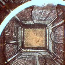
Port B is a 6-bit bi-directional I/O port with internal pull-up resistors (selected for each bit). The Port B output buffers have symmetrical drive characteristics with both high sink and source capability. As inputs, Port B pins that are externally pulled low will source current if the pull-up resistors are activated when recover pic16f876 Mcu.
The Port B pins are tri-stated when a reset condition becomes active, even if the clock is not running. Reset input. A low level on this pin for longer than the minimum pulse length will generate a reset, even if the clock is not running. The minimum pulse length is given in Table 23-3 on page 170. Shorter pulses are not guaranteed to generate a reset.
Some of the Status Flags are cleared by writing a logical one to them. Note that, unlike most other AVRs, the CBI and SBI before recover pic16f877 Mcu
I/O Registers within the address range 0x00 – 0x1F are directly bit-accessible using the SBI and CBI instructions. In these
For compatibility with future devices, reserved bits should be written to zero if accessed. Reserved I/O memory addresses should never be written when Break Mcu. registers, the value of single bits can be checked by using the SBIS and SBIC instructions. instructions will only operation the specified bit, and can therefore be used on registers containing such Status Flags. The CBI and SBI instructions work with registers 0x00 to 0x1F only.
PLL not locking
When at frequencies below 6.0 MHz, the PLL will not lock
Problem fix / Workaround
When using the PLL, run at 6.0 MHz or higher.
EEPROM break from application code does not work in Lock Bit Mode 3
When the Memory Lock Bits LB2 and LB1 are programmed to mode 3, EEPROM break does not work from the application code.
Problem Fix/Work around
Do not set Lock Bit Protection Mode 3 when the application code needs to break from EEPROM.
Breaking EEPROM at low frequency may not work for frequencies below 900 kHz
Breaking data from the EEPROM at low internal clock frequency may result in wrong data break.
Problem Fix/Workaround
Avoid using the EEPROM at clock frequency below 900kHz.
Timer Counter 1 PWM output generation on OC1B – XOC1B does not work correctly
Timer Counter1 PWM output OC1B-XOC1B does not work correctly. Only in the case when the control bits, COM1B1 and COM1B0 are in the same mode as COM1A1 and COM1A0, respectively, the OC1B-XOC1B output works correctly before Break Mcu.
Problem Fix/Work around
The only workaround is to use same control setting on COM1A(1:0) and COM1B(1:0) control bits, see table 14-4 in the data sheet. The problem has been fixed for Tiny45 rev D when Break Mcu.
Posted in Break IC |
Tags: break mcu source archive, break mcu source bin, break mcu source code, break mcu source content, break mcu source data, break mcu source eeprom, break mcu source file, break mcu source firmware, break mcu source hex, break mcu source information, break mcu source memory, break mcu source program |
Comments Closed
Break IC ATtiny84 Heximal
Break IC ATtiny84 protection and readout Heximal from attiny84 flash and eeprom memory, microcontroller attiny84 fuse bit will be unlocked;
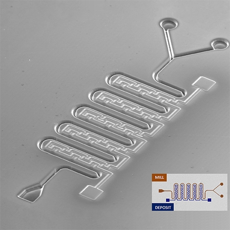
The ATtiny13A is a low-power CMOS 8-bit microcontroller based on the AVR enhanced RISC architecture. By executing powerful instructions in a single clock cycle, the ATtiny13A achieves throughputs approaching 1 MIPS per MHz allowing the system designer to optimize power consumption versus processing speed.
The AVR core combines a rich instruction set with 32 general purpose working registers. All 32 registers are directly connected to the Arithmetic Logic Unit (ALU), allowing two independent registers to be accessed in one single instruction executed in one clock cycle. The resulting architecture is more code efficient while achieving throughputs up to ten times faster than conventional CISC microcontrollers if Break pic12f609 IC.
The ATtiny13A provides the following features: 1K byte of In-System Programmable Flash, 64 bytes EEPROM, 64 bytes SRAM, 6 general purpose I/O lines, 32 general purpose working registers, one 8-bit Timer/Counter with compare modes, Internal and External Interrupts, a 4-channel, 10-bit ADC, a programmable Watchdog Timer with internal Oscillator, and three software selectable power saving modes. The Idle mode stops the CPU while allowing the SRAM, Timer/Counter, ADC, Analog Comparator, and Interrupt system to continue functioning.
The Power-down mode saves the register contents, disabling all chip functions until the next Interrupt or Hardware Reset. The ADC Noise Reduction mode stops the CPU and all I/O modules except ADC, to minimize switching noise during ADC conversions before Break pic12f639 IC.
The device is manufactured using Atmel’s high density non-volatile memory technology. The On-chip ISP Flash allows the Program memory to be re-programmed In-System through an SPI serial interface, by a conventional non-volatile memory programmer or by an On-chip boot code running on the AVR core.
The ATtiny13A AVR is supported with a full suite of program and system development tools including: C Compilers, Macro Assemblers, Program Debugger/Simulators, and Evaluation kits after attack mcu pic12f675.
A comprehensive set of drivers, application notes, data sheets and descriptions on development tools are available for download at http://www.atmel.com/avr. This documentation contains simple code examples that briefly show how to use various parts of the device.
These code examples assume that the part specific header file is included before compilation. Be aware that not all C compiler vendors include bit definitions in the header files and interrupt handling in C is compiler dependent. Please confirm with the C compiler documentation for more details when Break IC. Reliability Qualification results show that the projected data retention failure rate is much less than 1 PPM over 20 years at 85°C or 100 years at 25⋅C.
Posted in Break IC |
Tags: break ic source data, break ic source file, break ic source firmware, break ic source flash, break ic source heximal, break ic source software |
Comments Closed
Break MCU ATtiny24V Flash
Break MCU ATtiny24V security fuse bit and crack microcontroller attiny24v system against unauthorized reading, extract program from attiny24v mcu Flash and eeprom memory;
The AVR core combines a rich instruction set with 32 general purpose working registers. All the 32 registers are directly connected to the Arithmetic Logic Unit (ALU), allowing two independent registers to be accessed in one single instruction executed in one clock cycle when Break pld palce16v8 software.
The resulting architecture is more code efficient while achieving throughputs up to ten times faster than conventional CISC mcus.
The ATtiny24/44/84 provides the following features: 2/4/8K byte of In-System Programmable Flash, 128/256/512 bytes EEPROM, 128/256/512 bytes SRAM, 12 general purpose I/O lines, 32 general purpose working registers, a 8-bit Timer/Counter with two PWM channels, a 16-bit timer/counter with two PWM channels, Internal and External Interrupts, a 8-channel 10-bit ADC, programmable gain stage (1x, 20x) for 12 differential ADC channel pairs, a programmable Watchdog Timer with internal Oscillator, internal calibrated oscillator, and three software selectable power saving modes if Break pic16c717 mcu program.
The Idle mode stops the CPU while allowing the SRAM, Timer/Counter, ADC, Analog Comparator, and Interrupt system to continue functioning. The Power-down mode saves the register contents, disabling all chip functions until the next Interrupt or Hardware Reset before attack pic16c710 Mcu.
The ADC Noise Reduction mode stops the CPU and all I/O modules except ADC, to minimize switching noise during ADC conversions. In Standby mode, the crystal/resonator Oscillator is running while the rest of the device is sleeping. This allows very fast start-up combined with low power consumption.
The device is manufactured ng Atmel’s high density non-volatile memory technology. The On-chip ISP Flash allows the Program memory to be re-programmed In-System through an SPI serial interface, by a conventional non-volatile memory programmer or by an On-chip boot code running on the AVR core.
The ATtiny24/44/84 AVR is supported with a full suite of program and system development tools including: C Compilers, Macro Assemblers, Program Debugger/Simulators, In-Circuit Emulators, and Evaluation kits. Port B is a 4-bit bi-directional I/O port with internal pull-up resistors (selected for each bit) if recover pic16c74 Mcu code.
The Port B output buffers have symmetrical drive characteristics with both high sink and source capability except PB3 which has the RESET capability. To use pin PB3 as an I/O pin, instead of RESET pin, program (‘0’) RSTDISBL fuse. As inputs, Port B pins that are externally pulled low will source current if the pull-up resistors are activated.
The Port B pins are tri-stated when a reset condition becomes active, even if the clock is not running. Port A is a 8-bit bi-directional I/O port with internal pull-up resistors (selected for each bit). The Port A output buffers have symmetrical drive characteristics with both high sink and source capability.
As inputs, Port A pins that are externally pulled low will source current if the pull-up resistors are activated. The Port A pins are tri-stated when a reset condition becomes active, even if the clock is not running.
Posted in Break IC |
Tags: break mcu encrypted archive, break mcu encrypted binary, break mcu encrypted code, break mcu encrypted content, break mcu encrypted data, break mcu encrypted eeprom, break mcu encrypted file, break mcu encrypted firmware, break mcu encrypted heximal, break mcu encrypted information, break mcu encrypted memory, break mcu encrypted program |
Comments Closed
Break Chip ATmega48PA Firmware
Break Chip ATmega48PA tamper resistance system and readout the firmware from microcontroller atmega48pa flash memory, the mcu atmega48pa fuse bit will be broken when crack it;
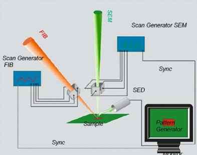
· High Performance, Low Power AVR® 8-Bit Microcontroller
· Advanced RISC Architecture
– 131 Powerful Instructions – Most Single Clock Cycle Execution
– 32 x 8 General Purpose Working Registers
– Fully Static Operation
– Up to 20 MIPS Throughput at 20 MHz
– On-chip 2-cycle Multiplier
– 4/8/16/32K Bytes of In-System Self-Programmable Flash progam memory (ATmega48PA/88PA/168PA/328P)
– 256/512/512/1K Bytes EEPROM (ATmega48PA/88PA/168PA/328P)
– 512/1K/1K/2K Bytes Internal SRAM (ATmega48PA/88PA/168PA/328P) if recover pic16f873 chip hex
– Write/Erase Cycles: 10,000 Flash/100,000 EEPROM
– Data retention: 20 years at 85°C/100 years at 25°C(1)
– Optional Boot Code Section with Independent Lock Bits
In-System Programming by On-chip Boot Program
True Read-While-Write Operation
– Programming Lock for Software Security
Peripheral Features
– Two 8-bit Timer/Counters with Separate Prescaler and Compare Mode
– One 16-bit Timer/Counter with Separate Prescaler, Compare Mode, and Capture
Mode
– Real Time Counter with Separate Oscillator before reocver mcu dspic30f6013a firmware
– Six PWM Channels
– 8-channel 10-bit ADC in TQFP and QFN/MLF package
Temperature Measurement
– 6-channel 10-bit ADC in PDIP Package
Temperature Measurement
– Programmable Serial USART
– Master/Slave SPI Serial Interface
– Byte-oriented 2-wire Serial Interface (Philips I2C compatible)
– Programmable Watchdog Timer with Separate On-chip Oscillator
– On-chip Analog Comparator
– Interrupt and Wake-up on Pin Change
Special Microcontroller Features
– Power-on Reset and Programmable Brown-out Detection if Break mcu at89c513a Chip
– Internal Calibrated Oscillator
– External and Internal Interrupt Sources
– Six Sleep Modes: Idle, ADC Noise Reduction, Power-save, Power-down, Standby, and Extended Standby I/O and Packages
– 23 Programmable I/O Lines
– 28-pin PDIP, 32-lead TQFP, 28-pad QFN/MLF and 32-pad QFN/MLF
Operating Voltage:
– 1.8 – 5.5V for ATmega48PA/88PA/168PA/328P
Temperature Range:
– -40°C to 85°C
Speed Grade:
– 0 – 20 MHz @ 1.8 – 5.5V
Low Power Consumption at 1 MHz, 1.8V, 25°C for ATmega48PA/88PA/168PA/328P:
Programmable Flash
ATmega48PA
ATmega88PA
ATmega168PA
ATmega328P
– Active Mode: 0.2 mA
– Power-down Mode: 0.1 µA
– Power-save Mode: 0.75 µA (Including 32 kHz RTC) before Break Chip
Break IC ATmega128A Firmware
Break IC ATmega128A to restore the Firmware from atmel microcontroller atmega128a flash and eeprom memory, the mcu atmega128a heximal file reading must be taken after the fuse bit has been reset;
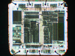
The Atmel QTouch Library provides a simple to use solution to realize touch sensitive interfaces on most Atmel AVR microcontrollers. The QTouch Library includes support for the QTouch and QMatrix acquisition methods. Touch sensing can be added to any application by linking the appropriate Atmel QTouch Library for the AVR Microcontroller. This is done by using a simple set of APIs to define the touch channels and sensors, and then calling the touch sensing API’s to retrieve the channel information and determine the touch sensor states.
The QTouch Library is FREE and downloadable from the Atmel website at the following location: www.atmel.com/qtouchlibrary. For implementation details and other information, refer to the Atmel QTouch Library User Guide – also available for download from the Atmel website. This datasheet contains simple code examples that briefly show how to use various parts of the device.
These code examples assume that the part specific header file is included before compilation. Be aware that not all C compiler vendors include bit definitions in the header files and interrupt handling in C is compiler dependent. Please confirm with the C compiler documentation for more details. For I/O registers located in extended I/O map, “IN”, “OUT”, “SBIS”, “SBIC”, “CBI”, and “SBI” instructions must be replaced with instructions that allow access to extended I/O. Typically “LDS” and “STS” combined with “SBRS”, “SBRC”, “SBR”, and “CBR”.
The Atmel QTouch Library provides a simple to use solution to realize touch sensitive interfaces on most Atmel AVR microcontrollers. The QTouch Library includes support for the QTouch and QMatrix acquisition methods. Touch sensing can be added to any application by linking the appropriate Atmel QTouch Library for the AVR Microcontroller.
This is done by using a simple set of APIs to define the touch channels and sensors, and then calling the touch sensing API’s to retrieve the channel information and determine the touch sensor states. The QTouch Library is FREE and downloadable from the Atmel website at the following location: www.atmel.com/qtouchlibrary. For implementation details and other information, refer to the Atmel QTouch Library User Guide – also available for download from the Atmel website if attacking mcu memory code.
Break MCU ATmega64PA Binary
Break MCU ATmega64PA and readout the embedded Binary from microcontroller atmega64pa flash memory, fuse bit of mcu atmega64pa will be crack to disable the protection;
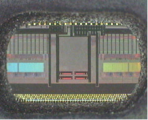
The ATmega64 is a highly complex mcu where the number of I/O locations supersedes the 64 I/O location reserved in the AVR instruction set. To ensure backward compatibility with the ATmega103, all I/O locations present in ATmega103 have the same location in ATmega64. Most additional I/O locations are added in an Extended I/O space starting from 0x60 to 0xFF (i.e., in the ATmega103 internal RAM space). These location can be reached by using LD/LDS/LDD and ST/STS/STD instructions only, not by using IN and OUT instructions. The relocation of the internal RAM space may still be a problem for ATmega103 users.
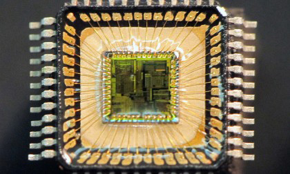
Also, the increased number of Interrupt Vectors might be a problem if the code uses absolute addresses. To solve these problems, an ATmega103 compatibility mode can be selected by programming the fuse M103C. In this mode, none of the functions in the Extended I/O space are in use, so the internal RAM is located as in ATmega103. Also, the extended Interrupt Vectors are removed. The ATmega64 is 100% pin compatible with ATmega103, and can replace the ATmega103 on current printed circuit boards. The application notes “Replacing ATmega103 by ATmega128” and “Migration between ATmega64 and ATmega128” describes what the user should be aware of replacing the ATmega103 by an ATmega128 or ATmega64PA.
By programming the M103C Fuse, the ATmega64 will be compatible with the ATmega103 regards to RAM, I/O pins and Interrupt Vectors as described above. However, some new features in ATmega64 are not available in this compatibility mode, these features are listed:
Pin Descriptions
One USART instead of two, asynchronous mode only. Only the eight least significant bits of the Baud Rate Register is available. One 16 bits Timer/Counter with two compare registers instead of two 16 bits Timer/Counters with three compare registers. Two-wire serial interface is not supported.
Port G serves alternate functions only (not a general I/O port). Port F serves as digital input only in addition to analog input to the ADC. Boot Loader capabilities is not supported. It is not possible to adjust the frequency of the internal calibrated RC Oscillator. The External Memory Interface can not release any Address pins for general I/O, neither configure different wait states to different External Memory Address sections. Only EXTRF and PORF exist in the MCUCSR Register. No timed sequence is required for Watchdog Timeout change. Only low-level external interrupts can be used on four of the eight External Interrupt sources. Port C is output only. USART has no FIFO buffer, so Data OverRun comes earlier. The user must have set unused I/O bits to 0 in ATmega103 programs after Break IC.
Posted in Break IC |
Tags: break mcu encrypted archive, break mcu encrypted code, break mcu encrypted content, break mcu encrypted data, break mcu encrypted eeprom, break mcu encrypted file, break mcu encrypted firmware, break mcu encrypted information, break mcu encrypted memory, break mcu encrypted program |
Comments Closed
Crack IC PIC12LC509 Security bits
Crack IC PIC12LC509 Security bits and decrypt microchip mcu pic12lc509 flash memory content out from it, extract secured code from pic12lc509 flash and eeprom memory in the format of heximal.
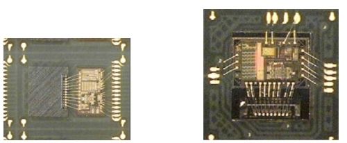
The MPLAB PM3 Device Programmer is a universal, CE compliant device programmer with programmable voltage verification at VDDMIN and VDDMAX for maximum reliability.
It features a large LCD display (128 x 64) for menus and error messages and a modular, detachable socket assembly to support various package types if recover mcu pic18f452 program.
The ICSP™ cable assembly is included as a standard item. In Stand-Alone mode, the MPLAB PM3 Device Programmer can read, verify and program PIC devices without a PC connection.
It can also set security bits protection in this mode. The MPLAB PM3 connects to the host PC via an RS-232 or USB cable.
The MPLAB PM3 has high-speed communications and optimized algorithms for quick programming of large memory devices and incorporates an SD/MMC card for file storage and secure data applications.
The PICSTART Plus Development Programmer is an easy-to-use, low-cost, prototype programmer. It connects to the PC via a COM (RS-232) port. MPLAB Integrated Development Environment software makes using the programmer simple and efficient if attack mcu tms320f241pg heximal.
The PICSTART Plus Development Programmer supports most PIC devices in DIP packages up to 40 pins. Larger pin count devices, such as the PIC16C92X and PIC17C76X, may be supported with an adapter socket.
The PICSTART Plus Development Programmer is CE compliant.
Posted in Break IC |
Tags: decap ic code, decap ic data, decap ic eeprom, decap ic file, decap ic firmware, decap ic lock bits, decap ic memory, decap ic program, decap ic security bits, decap ic software |
Comments Closed
Break Chip ATmega8A Binary
Break Chip ATmega8A and extract microcontroller atmega8a Binary from its flash memory, copy mcu atmega8a heximal out and then download to the new mcu to serve as the same functionality;
First Analog Comparator conversion may be delayed
If the device is powered by a slow rising VCC, the first Analog Comparator conversion will take longer than expected on some devices. Problem Fix/Workaround, When the device has been powered or reset, disable then enable theAnalog Comparator before the first conversion.
Interrupts may be lost when writing the timer registers in the asynchronous timer If one of the timer registers which is synchronized to the asynchronous timer2 clock is written in the cycle before a overflow interrupt occurs, the interrupt may be lost if attack atmega Chip flash memory.
Problem Fix/Workaround Always check that the Timer2 Timer/Counter register, TCNT2, does not have the value 0xFF before writing the Timer2 Control Register, TCCR2, or Output Compare Register, OCR2
Signature may be Erased in Serial Programming Mode If the signature bytes are read before a chiperase command is completed, the signature may be erased causing the device ID and calibration bytes to disappear. This is critical, especially, if the part is running on internal RC oscillator.
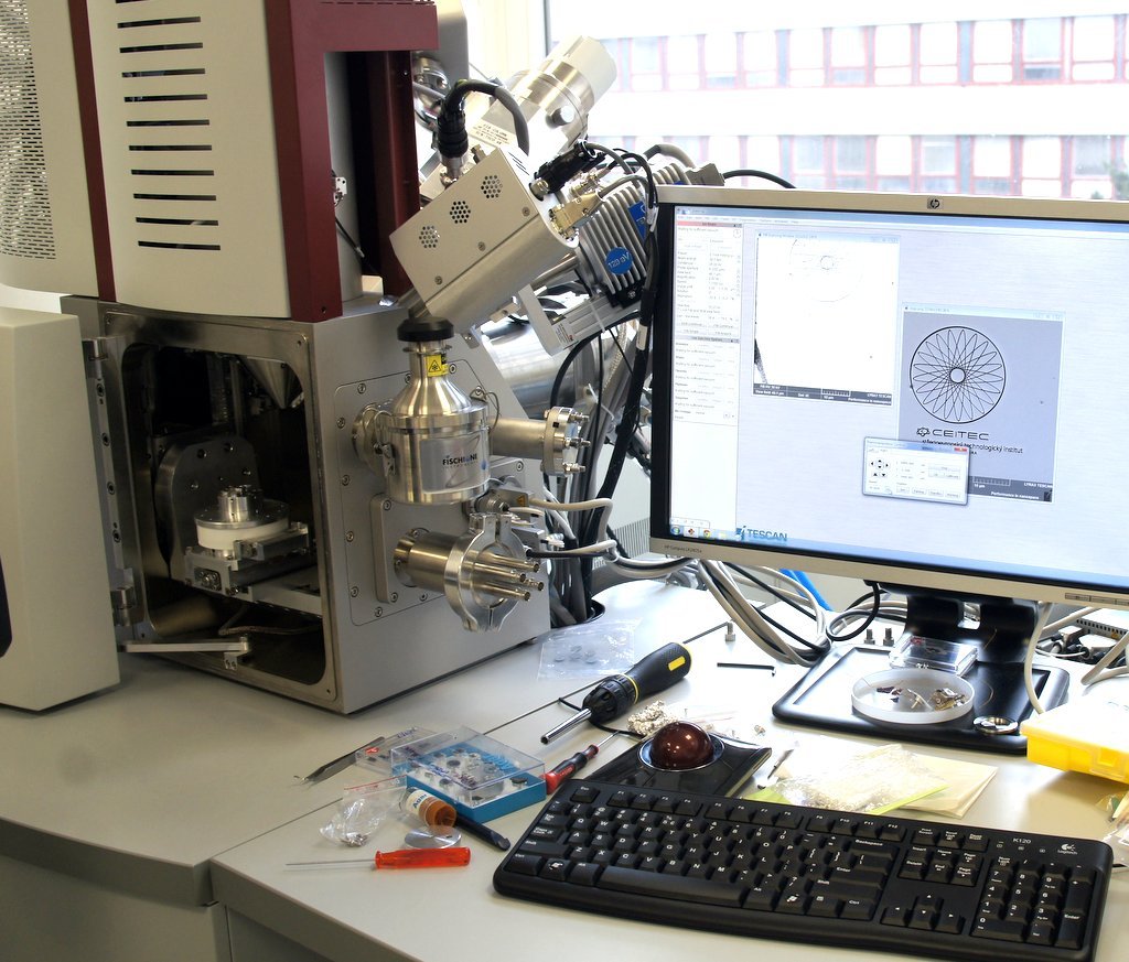
attack ATmega8A microprocessor protective system and restore heximal file from ATmega8A mcu flash memory
Problem Fix/Workaround: Ensure that the chiperase command has exceeded before applying the next command.
CKOPT Does not Enable Internal Capacitors on XTALn/TOSCn Pins when 32 KHz Oscillator is Used to Clock the Asynchronous Timer/Counter2 When the internal RC Oscillator is used as the main clock source, it is possible to run the Timer/Counter2 asynchronously by connecting a 32 KHz Oscillator between XTAL1/TOSC1 and XTAL2/TOSC2.
But when the internal RC Oscillator is selected as the main clock source, the CKOPT Fuse does not control the internal capacitors on XTAL1/TOSC1 and XTAL2/TOSC2. As long as there are no capacitors connected to XTAL1/TOSC1 and XTAL2/TOSC2, safe operation of the Oscillator is not guaranteed if attack dsp mcu Chip flash memory.
Problem fix/Workaround
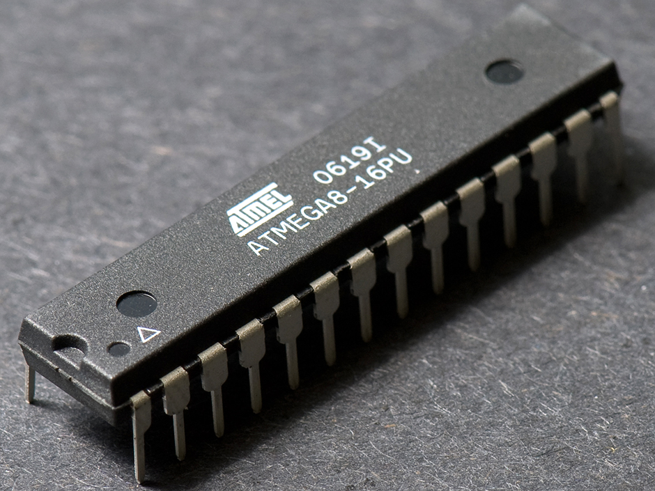
secured microcontroller atmega8a security fuse bit cracking to readout embedded program from atmega8a mcu flash memory
Use external capacitors in the range of 20 – 36 pF on XTAL1/TOSC1 and XTAL2/TOSC2. This will be fixed in ATmega8 Rev. G where the CKOPT Fuse will control internal capacitors also when internal RC Oscillator is selected as main clock source. For ATmega8 Rev. G, CKOPT = 0 (programmed) will enable the internal capacitors on XTAL1 and XTAL2. Customers who want compatibility between Rev.
G and older revisions, must ensure that CKOPT is unprogrammed (CKOPT = 1).
1
Updated Some Preliminary Test Limits and Characterization Data
The following tables have been updated:
Table 15, “Reset Characteristics,” on page 38, Table 16, “Internal Voltage Reference Characteristics,” on page 42, DC Characteristics on page 242, Table , “ADC Characteristics,” on page 248.
Changes in External Clock Frequency
Added the description at the end of “External Clock” on page 32.
Added period changing data in Table 99, “External Clock Drive,” on page 244.
Updated TWI Chapter
More details regarding use of the TWI bit rate prescaler and a Table 65, “TWI Bit
Rate Prescaler,” on page 173.
Updated Typical Start-up Times.
The following tables has been updated:
Table 5, “Start-up Times for the Crystal Oscillator Clock Selection,” on page 28,
Table 6, “Start-up Times for the Low-frequency Crystal Oscillator Clock Selection,”
on page 28, Table 8, “Start-up Times for the External RC Oscillator Clock Selection,” on page 29, and Table 12, “Start-up Times for the External Clock Selection,” on page 32 if Break Chip.
Posted in Break IC |
Tags: crack mcu atmega8a flash, microprocessore di attacco atmega8a, rompere la memoria del microcontrollore atmega8a |
Comments Closed
Clone Microcontroller PIC16C54 Heximal
Clone Microcontroller PIC16C54 Heximal is a process to duplicate microcontroller pic16c54 memory program from flash and eeprom, firmware will be extracted from mcu pic16c54 after break it;
Bit 15:12 – Reserved Bits
These bits are reserved for future use. For compatibility with future devices, these bit must be written to zero when UBRRH is written.
Bit 11:0 – UBRR11:0: USART Baud Rate Register
This is a 12-bit register which contains the USART baud rate. The UBRRH contains the four most significant bits, and the UBRRL contains the eight least significant bits of the USART baud rate if attack pic18f66k90 microcontroller hex.
Ongoing transmissions by the Transmitter and Receiver will be corrupted if the baud rate is changed. Writing UBRRL will trigger an immediate update of the baud rate prescaler.
For standard crystal and resonator frequencies, the most commonly used baud rates for asynchronous operation can be generated by using the UBRR settings in Table 106 to Table 109.
UBRR values which yield an actual baud rate differing less than 0.5% from the target baud rate, are bold in the table. Higher error ratings are acceptable, but the Receiver will have less noise resistance when the error ratings are high, especially for large serial frames (see “Asynchronous Operational Range” on page 220) when Copy pic18f458 MICROCONTROLLER hex.
The error values are calculated using the following equation:
BaudRateClosest Match
⎝ BaudRate ⎠
The Universal Synchronous and Asynchronous serial Receiver and Transmitter (USART) can be set to a master SPI compliant mode of operation. The Master SPI Mode (MSPIM) has the following features:
Full Duplex, Three-wire Synchronous Data Transfer
Master Operation
Supports all four SPI Modes of Operation (Mode 0, 1, 2, and 3)
LSB First or MSB First Data Transfer (Configurable Data Order)
Queued Operation (Double Buffered)
High Resolution Baud Rate Generator
High Speed Operation (fXCKmax = fCK/2)
Flexible Interrupt Generation
Posted in Break IC |
Tags: clone microcontroller bin, clone microcontroller code, clone microcontroller data, clone microcontroller eeprom, clone microcontroller file, clone microcontroller firmware, clone microcontroller fuse bit, clone microcontroller hex, clone microcontroller lock bit, clone microcontroller memory, clone microcontroller program, clone microcontroller software |
Comments Closed