Archive for the ‘Break IC’ Category
 MCU Crack Security Solution
 August 8th, 2012 |
  Author:
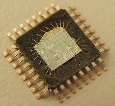
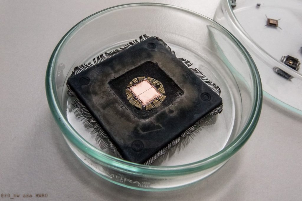
 MCU Crack Security Solution was to place the EEPROM data storage chip next to the MCU inside the same plastic package. To attack such a MCU is not easy; a professional would decapsulate the sample and either microprobe the data or bond it into a separate test package.
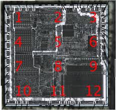
Both methods require equipment which cannot be afforded by a low-budget MCU Cracker. Such an MCU Cracker could try to use homemade microprobers (bonding pads on old chips are relatively large) or exploit a software bug to get access to the data.
Some microcontrollers do not have any special microcontroller hardware security protection at all. Their protection is based on obscurity of the proprietary programming algorithm. It might be the case that the read-back function was deliberately disguised, or replaced with a verify-only function.
Usually such MCUs do not offer very good protection and some examples are presented. In fact, the verify-only approach could be very powerful if implemented properly, as it is in some smartcards.
 Posted in Break IC |
  Tags: cpld mcu copy, dsp mcu copy, fpga mcu copy, mcu copy, pld mcu copy |
  Comments Closed
AVR Crack evolution in silicon chips
In the beginning there were almost no protection against avr crack of such devices except law and economics. For example, ROMs were made with low-cost mask technology and MCU Clone would involve either replacing them with EPROMs which are usually 3–10 times more expensive, or ordering Mask ROMs which would take time and require large capital investments. Another approach was used in game consoles where simple ASICs (Application-Specific Integrated Circuits) were widely used. Such ASICs were mainly carrying out I/O functions to replace tens of simple logic components, thus reducing the cost of the board and at the same time protecting against competitors who had to use larger and more expensive solutions. In fact these ASICs did not carry much security and their functionality could be understood in a few hours with a simple analysis of the signals using an oscilloscope or doing an exhaustive search over all possible combinations on their pins.
Break Secured MCU PIC16F72 Data
Break Secured MCU PIC16F72 and extract Data of microcontroller PIC16F72 from flash memory and eeprom memory, make Microprocessor PIC16F72 cloning through the process;
The internal RC oscillator provides a fixed 4 MHz (nominal) system clock at VDD = 5V and 25°C, see “Electrical Specifications” section for information on variation over voltage and temperature.
For the PIC16F72, bits <7:2>, CAL5- CAL0 are used for calibration. Adjusting CAL5-0 from 000000 to 111111 yields a higher clock speed.
Note that bits 1 and 0 of OSCCAL are unimplemented and should be written as 0 when modifying OSCCAL for compatibility with future devices before reverse engineering Secured MCU atmega2560v firmware.
For the PIC16F72, the upper 4 bits of the register are used. Writing a larger value in this location yields a higher clock speed. This configuration bit when unprogrammed (left in the ‘1’ state) enables the external MCLR function. When programmed, the MCLR function is tied to the internal VDD, and the pin is assigned to be a GPIO.
See Figure 8-7. When pin GP3/MCLR/VPP is configured as MCLR, the internal pull-up is always on.The PIC12C5XX family incorporates on-chip Power On Reset (POR) circuitry which provides an internal chip reset for most power-up situations.
The on-chip POR circuit holds the chip in reset until VDD has reached a high enough level for proper operation. To take advantage of the internal POR, program the GP3/MCLR/VPP pin as MCLR and tie through a resistor to VDD or program the pin as GP3 before reverse engineering microcontroller atmega1281 data.
An internal weak pull-up resistor is implemented using a transistor. Refer to Table 11-1 for the pull-up resistor ranges. This will eliminate external RC components usually needed to create a Power-on Reset.
A maximum rise time for VDD is specified. See Electrical Specifications for details. When the device starts normal operation (exits the reset condition), device operating parameters (voltage, frequency, temperature, …) must be met to ensure operation. If these conditions are not met, the device must be held in reset until the operating parameters are met.
Break IC PIC12F509 Eeprom
Break IC PIC12F509 Eeprom protection and extract hexiaml from MCU PIC12F509, reprogramme the firmware to new PIC12F509 microcontroller for cloning;
After generating a START condition, the bus master transmits a control byte consisting of a slave address and a Read/Write bit that indicates what type of operation is to be performed.
The slave address consists of a 4-bit device code (1010) followed by three don’t care bits. The last bit of the control byte determines the operation to be performed.
When set to a one a read operation is selected, and when set to a zero a write operation is selected. (Figure 7-5). The bus is monitored for its corresponding slave address all the time before recover chip pic12c508 software.
It generates an acknowledge bit if the slave address was true and it is not in a programming mode. Following the start signal from the master, the device code (4 bits), the don’t care bits (3 bits), and the R/W bit (which is a logic low) are placed onto the bus by the master transmitter.
This indicates to the addressed slave receiver that a byte with a word address will follow after it has generated an acknowledge bit during the ninth clock cycle. Therefore, the next byte transmitted by the master is the word address and will be written into the address pointer.
Only the lower four address bits are used by the device, and the upper four bits are don’t cares. The address byte is acknowledgeable and the master device will then transmit the data word to be written into the addressed memory location.
The memory acknowledges again and the master generates a stop condition. This initiates the internal write cycle, and during this time will not generate acknowledge signals. After a byte write command, the internal address counter will not be incremented and will point to the same address location that was just written.
If a stop bit is transmitted to the device at any point in the write command sequence before the entire sequence is complete, then the command will abort and no data will be written. If more than 8 data bits are transmitted before the stop bit is sent, then the device will clear the previously loaded byte and begin loading the data buffer again.
If more than one data byte is transmitted to the device and a stop bit is sent before a full eight data bits have been transmitted, then the write command will abort and no data will be written. The EEPROM memory employs a VCC threshold detector circuit which disables the internal erase/write logic if the VCC is below minimum VDD. Byte write operations must be preceded and immediately followed by a bus not busy bus cycle where both SDA and SCL are held high.
Posted in Break IC |
Tags: break protected ic binary, break protected ic code, break protected ic data, break protected ic eeprom, break protected ic file, break protected ic firmware, break protected ic flash, break protected ic heximal, break protected ic memory, break protected ic software |
Comments Closed
Decrypt Locked Chip PIC12F508 Firmware
Decrypt Locked Chip PIC12F508 Firmware from secured program memory and data memory, microcontroller PIC12F508 cracking will help to disable the protection and readout MCU PIC12F508 heximal.
The code for these functions is available on our website www.microchip.com. The code will be accessed by either including the source code FL51XINC.ASM or by linking FLASH5IX.ASM.
It is very important to check the return codes when using these calls, and retry the operation if unsuccessful. Unsuccessful return codes occur when the EE data memory is busy with the previous write, which can take up to 4 mS if copy chip pic16c73a program.
SDA is a bi-directional pin used to transfer addresses and data into and data out of the device. For normal data transfer SDA is allowed to change only during SCL low. Changes during SCL high are reserved for indicating the START and STOP conditions.
The EEPROM interface is a 2-wire bus protocol consisting of data (SDA) and a clock (SCL). Although these lines are mapped into the GPIO register, they are not accessible as external pins; only to the internal EEPROM peripheral after recover mcu pic16f74a binary.
SDA and SCL operation is also slightly different than GPO-GP5 as listed below. Namely, to avoid code overhead in modifying the TRIS register, both SDA and SCL are always outputs.
To decrypt data from the EEPROM peripheral requires outputting a ‘1’ on SDA placing it in high-Z state, where only the internal 100K pull-up is active on the SDA line.
This code must reside in the lower half of a page. The code achieves it’s small size without additional calls through the use of a sequencing table. The table is a list of procedures that must be called in order.
The table uses an ADDWF PCL,F instruction, effectively a computed goto, to sequence to the next procedure. However the ADDWF PCL,F instruction yields an 8 bit address after recover chip pic16c71 code,
The following bus protocol is to be used with the EEPROM data memory.
Data transfer may be initiated only when the bus is not busy.
During data transfer, the data line must remain stable whenever the clock line is HIGH. Changes in the data line while the clock line is HIGH will be interpreted as a period of the clock signal. There is one bit of data per clock pulse.
Each data transfer is initiated with a START condition and terminated with a STOP condition. The number of the data bytes transferred between the START and STOP conditions is determined by the master device and is theoretically unlimited if Decrypt locked Chip Firmware. A HIGH to LOW transition of the SDA line while the clock (SCL) is HIGH determines a START condition. All commands must be preceded by a START condition. A LOW to HIGH transition of the SDA line while the clock (SCL) is HIGH determines a STOP condition. All operations must be ended with a STOP condition.
Posted in Break IC |
Tags: decrypt locked chip bin, decrypt locked chip code, decrypt locked chip data, decrypt locked chip eeprom, decrypt locked chip file, decrypt locked chip firmware, decrypt locked chip hex, decrypt locked chip memory, decrypt locked chip program, decrypt locked chip software |
Comments Closed
Break IC PIC16LF54 Protection
Break IC PIC16LF54 Protection and extract code from MCU PIC16LF54, crack Microcontroller PIC16LF54 fuse bit and decapsulate package;
When a prescaler is used, the external clock input is divided by the asynchronous ripple counter-type prescaler so that the prescaler output is symmetrical.
For the external clock to meet the sampling requirement, the ripple counter must be taken into account. Therefore, it is necessary for T0CKI to have a period of at least 4TOSC (and a small RC delay of 40 ns) divided by the prescaler value if recover chip pic16hv785 hex.
The only requirement on T0CKI high and low time is that they do not violate the minimum pulse width requirement of 10 ns. Refer to parameters 40, 41 and 42 in the electrical specification of the desired device.
Since the prescaler output is synchronized with the internal clocks, there is a small delay from the time the external clock edge occurs to the time the Timer0 module is actually incremented before recover chip pic16c621 program.
Figure 6-4 shows the delay from the external clock edge to the timer incrementing. If the option register is set to read TIMER0 from the pin, the port is forced to an input regardless of the TRIS register setting.
The prescaler assignment is fully under software control (i.e., it can be changed “on the fly” during program execution). To avoid an unintended device RESET, the following instruction sequence (Example 6-1) must be executed when changing the prescaler assignment from Timer0 to the WDT when Break IC pic16f621a program.
The PIC16LF54 each have 16 bytes of EEPROM data memory. The EEPROM memory has an endurance of 1,000,000 erase/write cycles and a data retention of greater than 40 years.
The EEPROM data memory supports a bi-directional 2-wire bus and data transmission protocol. These two-wires are serial data (SDA) and serial clock (SCL), that are mapped to bit6 and bit7, respectively, of the GPIO register (SFR 06h) after recover mcu pic16c622a software.
Unlike the GP0-GP5 that are connected to the I/O pins, SDA and SCL are only connected to the internal EEPROM peripheral. For most applications, all that is required is calls to the following functions;
Reverse Locked IC PIC16F54 Firmware
Reverse Locked IC PIC16F54 manufacturing process and extract IC PIC16F54 Firmware from secured program and data memory by cracking PIC16F54 eeprom and flash memory;
The output driver control register is loaded with the contents of the W register by executing the TRIS instruction. A ‘1’ from a TRIS register bit puts the corresponding output driver in a hi-impedance mode.
A ‘0’ puts the contents of the output data latch on the selected pins, enabling the output buffer. The exceptions are GP3 which is input only and GP2 which may be controlled by the option register,
A read of the ports reads the pins, not the output data latches. That is, if an output driver on a pin is enabled and driven high, but the external system is holding it low, a read of the port will indicate that the pin is low.
The TRIS registers are “write-only” and are set (output drivers disabled) upon RESET. Some instructions operate internally as read followed by write operations after Recover IC PIC12LC508A eeprom.
The BCF and BSF instructions, for example, read the entire port into the CPU, execute the bit operation and re-write the result. Caution must be used when these instructions are applied to a port example.
a BSF operation on bit5 of GPIO will cause directional I/O pin (say bit0) and it is defined as an input at this time, the input signal present on the pin itself would be read into the CPU and rewritten to the data latch of this particular pin, overwriting the where one or more pins are used as input/outputs if copy protected chip pic16c56 code.
For previous content. As long as the pin stays in the input mode, no problem occurs. However, if bit0 is switched into output mode later on, the content of the data latch maybe unknown.
Posted in Break IC |
Tags: reverse locked ic binary, reverse locked ic code, reverse locked ic data, reverse locked ic eeprom, reverse locked ic file, reverse locked ic firmware, reverse locked ic heximal, reverse locked ic memory, reverse locked ic program, reverse locked ic software |
Comments Closed
Extract Microprocessor PIC16C58B Data
Extract Microprocessor PIC16C58B Data from eeprom after unlock microcontroller PIC16C58B secured memory, and copy program pic16c58b into new MCU;
PIC16C58B devices have a 12-bit wide L.I.F.O. hardware push/pop stack. A CALL instruction will push the current value of stack 1 into stack 2 and then push the current data counter value, incremented by one, into stack level 1.
If more than two sequential CALL’s are executed, only the most recent two return addresses are stored. ARETLW instruction will pop the contents of stack level 1 into the data counter and then extract stack level 2 contents into level 1.
If more than two sequential RETLW’s are executed, the stack will be filled with the address previously stored in level 2. Note that the W register will be loaded with the literal value specified in the instruction.
This is particularly useful for the implementation of data look-up tables within the data memory. Upon any reset, the contents of the stack remain unchanged, however the data counter (PCL) will also be reset to 0 after copy Microprocessor PIC16F74 code.
The INDF register is not a physical register. Addressing INDF actually addresses the register As with any other register, the I/O register can be written and read under data control.
However, read instructions (e.g., MOVF GPIO,W) always read the I/O pins independent of the pin’s input/output modes. On RESET, all I/O ports are defined as input (inputs are at hi-impedance) since the I/O control registers are all set.
See Section 7.0 for SCL and SDA description for PIC16C58B. GPIO is an 8-bit I/O register. Only the low order 6 bits are used (GP5:GP0). Bits 7 and 6 are unimplemented and read as ‘0’s before break IC PIC16F914 heximal.
Please note that GP3 is an input only pin. The configuration word can set several I/O’s to alternate functions. When acting as alternate functions the pins will read as ‘0’ during port read.
Pins GP0, GP1, and GP3 can be configured with weak pull-ups and also with wake-up on change. The wake-up on change and weak pull-up functions are not pin selectable. If pin 4 is configured as MCLR, weak pull-up is always on and wake-up on change for this pin is not enabled.
Posted in Break IC |
Tags: extract microprocessor binary, extract microprocessor code, extract microprocessor content, extract microprocessor data, extract microprocessor eeprom, extract microprocessor file, extract microprocessor firmware, extract microprocessor heximal, extract microprocessor memory, extract microprocessor program, extract microprocessor software |
Comments Closed
Crack DSP will damage original mother chip’s code?
Currently we have 2 ways to crack dsp code, 1 is base upon software, which has been called un-intrusive dsp code crack, it will apply software such as self-made programmer, and this method won’t damage sample during the crack dsp code process ( but the dsp mcu will under the state of decryption after recovery );
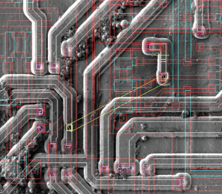
Another method is base upon hardware affiliate with software, so call intrusive crack dsp code, this method will need to open the cover package outside chip which is being widely known as DECAPSULATION and then do the circuit modification so call FIB, abbreviation of FOCUSED ION BEAM, destroy the profile structure and die circuit won’t affect its functions, just the encryption status.
Posted in Break IC |
Tags: dsp attack, dsp break, dsp decryption, dsp extraction, dsp hack, dsp recover |
Comments Closed
Break IC ATmega88V Internal Flash
We can break IC ATMEGA88V internal flash, please view the IC ATMEGA88V features for your reference:
This documentation contains simple internal flash examples that briefly show how to use various parts of the device. These internal flash examples assume that the part specific header file is included before compilation. Be aware that not all C compiler vendors include bit definitions in the header files and interrupt handling in C is compiler dependent.
Please confirm with the C compiler documentation for more details. For I/O Registers located in extended I/O map, “IN”, “OUT”, “SBIS”, “SBIC”, “CBI”, and “SBI” instructions must be replaced with instructions that allow access to extended I/O. Typically “LDS” and “STS” combined with “SBRS”, “SBRC”, “SBR”, and “CBR”.
This section discusses the AVR core architecture in general. The main function of the CPU core is to ensure correct program execution. The CPU must therefore be able to access memories, perform calculations, control peripherals, and handle interrupts before Break IC ATmega88V Internal Flash.
In order to maximize performance and parallelism, the AVR uses a Harvard architecture – with separate memories and buses for program and data. Instructions in the program memory are executed with a single level pipelining. While one instruction is being executed, the next instruction is pre-fetched from the program memory.
This concept enables instructions to be executed in every clock cycle. The program memory is In-System Reprogrammable Flash memory. The fast-access Register File contains 32 x 8-bit general purpose working registers with a single clock cycle access time. This allows single-cycle Arithmetic Logic Unit (ALU) operation. In a typical ALU operation, two operands are output from the Register File, the operation is executed, and the result is stored back in the Register File – in one clock cycle.
Six of the 32 registers can be used as three 16-bit indirect address register pointers for Data Space addressing – enabling efficient address calculations. One of the these address pointers can also be used as an address pointer for look up tables in Flash program memory. These added function registers are the 16-bit X-, Y-, and Z-register, described later in this section before Break IC ATmega88V Internal Flash.
The ALU supports arithmetic and logic operations between registers or between a constant and a register. Single register operations can also be executed in the ALU. After an arithmetic operation, the Status Register is updated to reflect information about the result of the operation.
Program flow is provided by conditional and unconditional jump and call instructions, able to directly address the whole address space. Most AVR instructions have a single 16-bit word format. Every program memory address contains a 16- or 32-bit instruction.
Program Flash memory space is divided in two sections, the Boot Program section and the Application Program section. Both sections have dedicated Lock bits for write and read/write protection. The SPM instruction that writes into the Application Flash memory section must reside in the Boot Program section when Break IC ATmega88V Internal Flash.