Archive for the ‘Break IC’ Category
 MCU Code Reverse Engineering Roadmap
 August 17th, 2012 |
  Author:
 MCU Code Reverse Engineering is actually a process of reprogramming microcontroller in the reverse order, microcontroller will be reset by unlocking technique to ensure the heximal reading from flash memory;
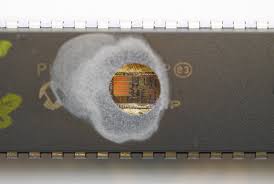
Technological progress on its own is increasing the costs to MCU reverse engineering. Ten years ago it was possible to use a laser cutter and a simple probing station to get access to any point on the chip surface, but for modern deep submicron semiconductor chips very sophisticated and expensive technologies must be used.
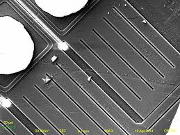
That excludes most potential MCU code extraction. For example, the structure of the Microchip PIC16F877 microcontroller can be easily observed and reverse engineered under a microscope.
The second metal layer and polysilicon layer can still be seen even if buried under the top metal layer. This is possible because each subsequent layer in the fabrication process follows the shape of the previous layer. Under a microscope the observer sees not only the highest layer but also edges that reveal the structure of the deeper layers.
In 0.5 µm and smaller technologies, for example in the Microchip PIC16F877A microcontroller, each predecessor layer is planarised using chemical-mechanical planarisation (CMP) process before applying the next layer. As a result the top metal layer does not show the impact of the deeper layers. The only way to reveal the structure of the deeper layers is by removing the top metal layers either mechanically or chemically.
As can be seen from all the shown examples, hardware security in microcontrollers and smartcards is being constantly improved. Because the tools for mcu code reverse engineering are becoming more sophisticated, better and better security protection is required. Rapid co-evolution is driven by this continuous battle between mcu manufacturers and mcu code reverse engineer.
Another threat that must be considered is that a great deal of second-hand semiconductor manufacturing and testing equipment appears on the market. It cannot be used to reverse engineering high-end products, but should be enough to reverse engineering MCUs manufactured with older technology. For example, while 90 nm manufacturing technology is currently leading-edge, most microcontrollers are produced with 0.35 µm technology and smartcards with 0.25 µm technology.
Break IC PIC16LF74 Memory
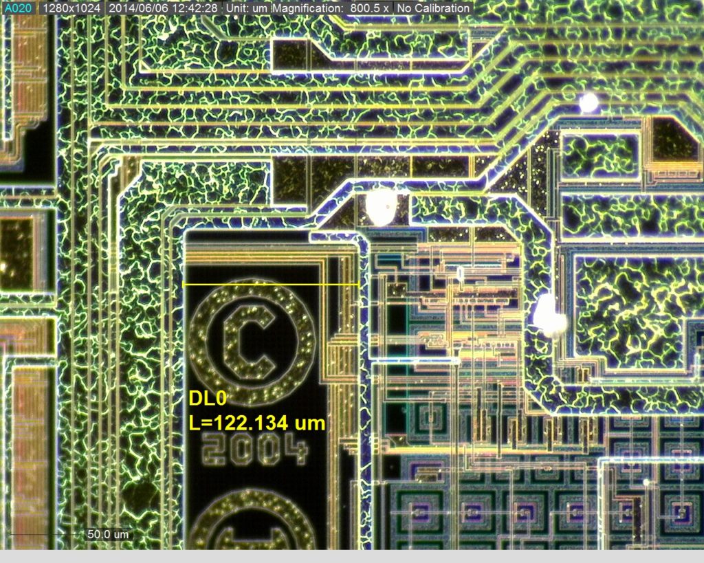
Break IC PIC16LF74 Memory needs to cut off security fuse bit by focus ion beam and readout microcontroller PIC16LF74 progrm;
High performance RISC CPU
Only 35 single word instructions to learn
All single cycle instructions except for program branches which are two-cycle
Operating speed: DC – 20 MHz clock input DC – 200 ns instruction cycle when Break IC
Up to 8K x 14 words of FLASH Program Memory, Up to 368 x 8 bytes of Data Memory (RAM)
Pinout compatible to the PIC16LF74
Pinout compatible to the PIC16LF74
Interrupt capability (up to 12 sources)
Eight level deep hardware stack
Direct, Indirect and Relative Addressing modes
Brown-out detection circuitry for
Parallel Slave Port (PSP), 8-bits wide with Universal Synchronous Asynchronous Receiver 8-bit, up to 8-channel Analog-to-Digital converter
Synchronous Serial Port (SSP) with SPI (Master
Timer2: 8-bit timer/counter with 8-bit period
Timer0: 8-bit timer/counter with 8-bit prescaler
Timer1: 16-bit timer/counter with prescaler,
Programmable memory protection
Power saving SLEEP mode
Selectable oscillator options before Break IC
In-Circuit Serial Programming (ICSP) via two
Watchdog Timer (WDT) with its own on-chip RC
Power-on Reset (POR)
Power-up Timer (PWRT) and Processor read access to program memory Oscillator Start-up Timer (OST) oscillator for reliable operation pins can be incremented during SLEEP via external crystal/clock register, prescaler and postscaler
Two Capture, Compare, PWM modules
– Capture is 16-bit, max. resolution is 12.5 ns
– Compare is 16-bit, max. resolution is 200 ns
– PWM max. resolution is 10-bit mode) and I2C (Slave) Transmitter (USART/SCI) external RD, WR and CS controls (40/44-pin only) Brown-out Reset (BOR)
Low power, high speed CMOS FLASH technology
Fully static design
Wide operating voltage range: 2.0V to 5.5V
High Sink/Source Current: 25 mA
Industrial temperature range
Low power consumption:
– < 2 mA typical @ 5V, 4 MHz
– 20 µA typical @ 3V, 32 kHz
– < 1 µA typical standby current
IC Code Break Intermediate Approach
IC Code Break is a process to crack microcontroller protective system and readout firmware from MCU embedded memory;
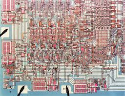
More often an intermediate approach is used when the IC is built from separate blocks but each block uses glue logic design as in, for example, the Cypress CY7C63001A microcontroller.
In this case an MCU breaker could more easily trace the bus and control lines between the blocks, and launch invasive or semi-invasive MCU attacking on the chip. Glue logic design does not eliminate the possibility of non-invasive cracking, but as the performance increases, faster and more expensive equipment is required.
Semi-invasive ic breaking will also face problems due to disguised design blocks. Of course the breaker could automate the process by running an exhaustive search and trying to break all possible areas. Definitely this approach would take a long time and may in the end not be successful. On the other hand, an mcu heximal extraction could be applied directly to the memory itself or its control circuit, because they cannot be implemented in the same glue logic structure and stay visibly separate.
 Posted in Break IC |
  Tags: cpld mcu source code break, dsp mcu source code break, fpga mcu source code break, pld mcu source code break |
  Comments Closed
Crack IC Code other Improvement
Crack IC Code other Improvement will make it become more expensive involve using a top metal sensor mesh. All paths in this mesh are continuously monitored for interruptions and short circuits, and cause reset or zeroing of the EEPROM memory if alarmed.
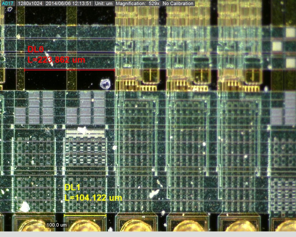
Normally such protection is not used in ordinary microcontrollers because, firstly, it increases the design cost and, secondly, it can be triggered unintentionally in abnormal working conditions such as high electromagnetic noise, low or high temperatures, irregular clock signal or power supply interruptions.
Instead, ordinary microcontrollers adopt the less expensive approach of placing a fake top layer mesh, but this still remains a very effective annoyance for optical analysis and microprobing IC code extraction. In smartcards such meshes are implemented properly with the sensor wires going between the power supply and ground wires.
Some design flaws were found in such implementations making microprobing program reading possible. Also such meshes do not protect against non-invasive mcu break, and some semi-invasive microcontroller crack are still possible because the mesh has gaps between the wires and light can pass through it down to the active areas of the circuit.
Posted in Break IC |
Tags: cpld mcu source code crack, dsp mcu source code crack, fpga mcu source code crack, mcu source code crack, pld mcu source code crack |
Comments Closed
Break Encrypted IC PIC16F76 Eeprom
Break Encrypted IC PIC16F76 Eeprom and flash memory, extract code from MCU PIC16F76 and copy firmware to new Microcontroller which will provide the same functions as original master processor;
Each PIC12C5XX instruction is a 12-bit word divided into an OPEEPROM, which specifies the instruction type, and one or more operands which further specify the operation of the instruction.
The PIC12C5XX instruction set summary in Table 9-2 groups the instructions into byte-oriented, bit-oriented, and literal and control operations. Table 9-1 shows the opeeprom field descriptions if recover pic16c505 encrypted Eeprom.
For byte-oriented instructions, ’f’ represents a file register designator and ’d’ represents a destination designator. The file register designator is used to specify which one of the 32 file registers is to be used by the instruction.
The destination designator specifies where the result of the operation is to be placed. If ’d’ is ’0’, the result is placed in the W register. If ’d’ is ’1’, the result is placed in the file register specified in the instruction.
Byte-oriented file register operations
For bit-oriented instructions, ’b’ represents a bit field designator which selects the number of the bit affected by the operation, while ’f’ represents the number of the file in which the bit is located when clone microcontroller pic16c54 heximal.
For literal and control operations, ’k’ represents an 8 or 9-bit constant or literal value.
All instructions are executed within a single instruction cycle, unless a conditional test is true or the program counter is changed as a result of an instruction.
In this case, the execution takes two instruction cycles. One instruction cycle consists of four oscillator periods. Thus, for an oscillator frequency of 4 MHz, the normal instruction execution time is 1 µs.
If a conditional test is true or the program counter is changed as a result of an instruction, the instruction execution time is 2 µs. Figure 9-1 shows the three general formats that the instructions can have. All examples in the figure use the following format to represent a hexadecimal number.
Further Improvement in Copy IC Code
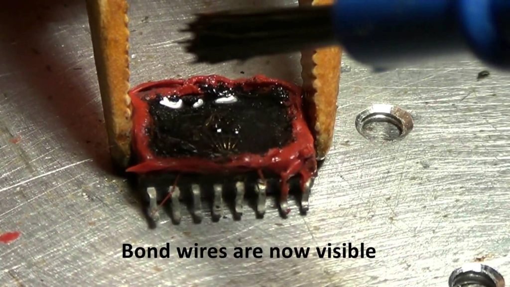
Copy IC Code Further Improvement involved using a part of the main memory to control access to the data from outside. This was implemented either by latching the information stored at a certain address at power-up and treating it as a security fuse, or by using passwords to grant access to the memory.
For example, in the Texas Instruments MSP430F112 microcontroller, the read-back operation can be called only after the correct 32-bytes password is entered. Without that, only the chip erase operation is available. Although such protection seems to be more effective than previous offerings, it has some drawbacks which could be exploited in low-cost non-invasive mcu cracking such as timing microcontroller program reading and power analysis.
More details on these mcu flash recovery are presented in later articles. If the state of the security fuse is sampled from the memory during power-up or reset, it could present some room for the ic code copier to play with power glitches, trying to force the circuit to get the wrong state of the memory.
 Posted in Break IC |
Tags: copy mcu source code, cpld mcu source code copy, dsp mcu source code copy, fpga mcu source code copy, pld mcu source code copy |
Comments Closed
Posted in Break IC |
Tags: copy mcu source code, cpld mcu source code copy, dsp mcu source code copy, fpga mcu source code copy, pld mcu source code copy |
Comments Closed
Break Locked Chip PIC16F74 Data
Break Locked Chip PIC16F74 program memory and readout MCU Data from eeprom memory, the heximal file can be rewritten to the new microcontroller PIC16F74 for IC cloning;
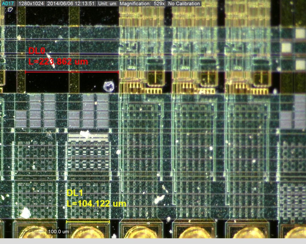
If the data protection bit has not been programmed, the on-chip program memory can be read out for verification process. The first 64 locations can be read by the PIC16F74 regardless of the data protection bit setting.
The last memory location cannot be read if data protection is enabled on the PIC16F74. The last memory location can be read regardless of the data protection bit setting on the PIC16F74 if recover microprocessor atmega1281pa flash.
Four memory locations are designated as ID locations where the user can store checksum or other data-identification numbers. These locations are not accessible during normal execution but are readable and writable during program/verify.
Use only the lower 4 bits of the ID locations and always program the upper 8 bits as ’0’s. The PIC16F74 locked chips with EPROM program memory can be serially programmed while in the end application circuit before Break ic atmega2560pa heximal.
This is simply done with two lines for clock and data, and three other lines for power, ground, and the programming voltage. This allows customers to manufacture boards with unprogrammed devices, and then program the locked chip just before shipping the product.
This also allows the most recent firmware or a custom firmware to be programmed. The device is placed into a program/verify mode by holding the GP1 and GP0 pins low while raising the MCLR (VPP) pin from VIL to VIHH (see programming specification).
GP1 becomes the programming clock and GP0 becomes the programming data. Both GP1 and GP0 are Schmitt Trigger inputs in this mode if Break mcu atmega2560l flash.
After reset, a 6-bit command is then supplied to the device. Depending on the command, 14-bits of program data are then supplied to or from the device, depending if the command was a load or a read. For complete details of serial programming, please refer to the PIC12C5XX Programming Specifications. A typical in-circuit serial programming connection is shown in Figure 8-16.
Posted in Break IC |
Tags: break locked chip bin, break locked chip code, break locked chip data, break locked chip eeprom, break locked chip file, break locked chip firmware, break locked chip flash, break locked chip hex, break locked chip memory, break locked chip program, break locked chip software |
Comments Closed
Break MCU PIC16LF73 Heximal
Break MCU PIC16LF73 security fuse bit and extract program from microcontroller PIC16LF73 memory, clone Heximal file to processor;
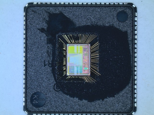
A device may be powered down (SLEEP) and later powered up (Wake-up from SLEEP). The Power-Down mode is entered by executing a SLEEP instruction.
If enabled, the Watchdog Timer will be cleared but keeps running, the TO bit (STATUS<4>) is set, the PD bit (STATUS<3>) is cleared and the oscillator driver is turned off if recover microprocessor atmega1280pa flash heximal.
The I/O ports maintain the status they had before the SLEEP instruction was executed (driving high, driving low, or hi-impedance). It should be noted that a RESET generated by a WDT time-out does not drive the MCLR pin low.
For lowest current consumption while powered down, the T0CKI input should be at VDD or VSS and the GP3/MCLR/VPP pin must be at a logic high level (VIHMC) if MCLR is enabled after Break reverse engineering MCU atmega48pv code.
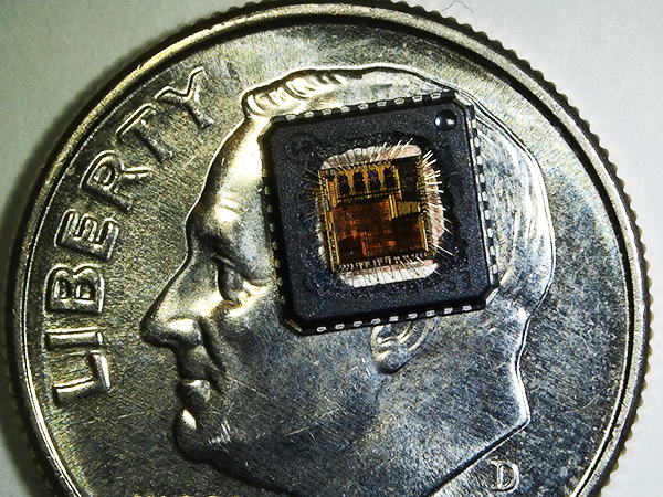
The device can wake-up from SLEEP through one of the following events:
An external reset input on GP3/MCLR/VPP pin, when configured as MCLR. A Watchdog Timer time-out reset (if WDT was enabled). A change on input pin GP0, GP1, or GP3/MCLR/VPP when wake-up on change is enabled.
These events cause a device reset. The TO, PD, and GPWUF bits can be used to determine the cause of device reset. The TO bit is cleared if a WDT time-out occurred (and caused wake-up).
The PD bit, which is set on power-up, is cleared when SLEEP is invoked. The GPWUF bit indicates a change in state while in SLEEP at pins GP0, GP1, or GP3 (since the last time there was a file or bit operation on GP port) before recover MCU atmega88pv firmware.
Caution: Right before entering SLEEP, read the input pins. When in SLEEP, wake up occurs when the values at the pins change from the state they were in at the last reading. If a wake-up on change occurs and the pins are not read before reentering SLEEP, a wake up will occur immediately even if no pins change while in SLEEP mode. The WDT is cleared when the device wakes from sleep, regardless of the wake-up source.
Posted in Break IC |
Tags: recover locked mcu bin, recover locked mcu code, recover locked mcu data, recover locked mcu eeprom, recover locked mcu file, recover locked mcu firmware, recover locked mcu flash, recover locked mcu heximal, recover locked mcu memory, recover locked mcu program, recover locked mcu software |
Comments Closed
Hack IC Code through Security Fuse
Hack IC Code through Security Fuse is a method suits for a part of microcontroller unlocking such as ATmel and Microchip MCUs, the security fuse bit normally embed in the memory;
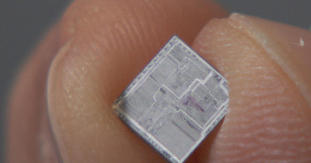
The next step was to make the security fuse part of the memory access circuit, so that any external access to the data is disabled if the fuse is set. Usually the fuse is located very close to the main MCU memory or evhen shares some control lines with it. Also it is fabricated with the same technology as the main MCU memory array making it harder to locate and reset.
Non-invasive IC firmware hacking could still exist but would require much time and effort to find. At the same time, semi-invasive MCU crack might still work. Certainly it would take more time for engineer to find the security fuse or the part of the control circuit responsible for the security monitoring, but this could be easily automated. Performing invasive IC code attack could be more difficult as most of the work would need to be done manually, so it will certainly increase the cost and time to extract IC code.
Posted in Break IC |
Tags: cpld mcu source code hack, dsp mcu source code hack, fpga mcu source code hack, hack mcu source code, pld mcu source code hack |
Comments Closed
Add Security Fuse to Prevent IC Code Attack
Add Security Fuse to Prevent IC Code Attack is commonly used way to extract embedded firmware from MCU flash and eeprom memory;
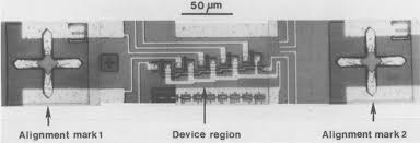
The next step in increasing the security protection against IC code attack which was in adding a hardware security fuse that disables the access to data.
The easiest implementation, which does not require the complete redesign of the microcontroller structure, was for the fuse to control the read-back function of the programming interface.
The drawback of this approach was in making it easier to locate the security fuse and perform an invasive MCU breaking. For example, the state of the fuse could be changed by connecting the output from the fuse cell directly to the power supply or ground line.
In some cases it might be enough to just disconnect the sense circuit from the fuse cell by cutting the wire from it with a laser cutter or focused ion beam (FIB) machine.
It might be possible to succeed in non-invasive mcu code extraction as well, because a separate fuse would certainly behave differently from the normal memory array. As a result it might be possible to find such a combination of external signals under which the state of this fuse would not be read correctly thus allowing the access to the information stored in the on-chip memory.
Semi-invasive MCU cracking could bring the code reading to success even faster but will require decapsulation of the chip to get access to the die. A well known example of such attacks is erasing the security fuse under a UV light.
Posted in Break IC |
Tags: cpld mcu source code attack, dsp mcu source code attack, fpga mcu source code attack, mcu source code attack, pld mcu source code attack |
Comments Closed