Archive for the ‘Break IC’ Category
 Break Microcontroller Samsung S3F9454 Software
 March 31st, 2014 |
  Author:
 Break Microcontroller Samsung S3F9454 locked memory and extract MCU S3F9454 software from flash memory, the program will be cloned from Microprocessor through universal programmer, an adaptive socket will be required for the whole process;
Break Microcontroller Samsung S3F9454 locked memory and extract MCU S3F9454 software from flash memory, the program will be cloned from Microprocessor through universal programmer, an adaptive socket will be required for the whole process
The SAM88RCRI instruction set is designed to support the large register file. It includes a full complement of 8-bit arithmetic and logic operations. There are 41 instructions. No special I/O instructions are necessary because I/O control and data registers are mapped directly into the register file. Flexible instructions for bit addressing, rotate, and shift operations complete the powerful data manipulation capabilities of the SAM88RCRI instruction set when break Microcontroller.
![Мікроконтролер Samsung S3F9454 широко використовується в промисловому, автомобільному та побутовому електроніці завдяки розширеним функціям та закріпленій вбудованій програмній програмі. Однак, коли прошивка, двійкова або EEPROM пам'яті заблокована або зашифрована, доступ до початкового вихідного коду стає проблемою. У [назві вашої компанії] ми спеціалізуємось на порушенні програмного забезпечення для мікроконтролера Samsung S3F9454, допомагаючи клієнтам розшифрувати, витягнути та відновити захищені дані для оптимізації системи, налагодження чи міграції.](https://www.ic-crack.com/wp-content/uploads/2014/03/3.png)
Мікроконтролер Samsung S3F9454 широко використовується в промисловому, автомобільному та побутовому електроніці завдяки розширеним функціям та закріпленій вбудованій програмній програмі. Однак, коли прошивка, двійкова або EEPROM пам’яті заблокована або зашифрована, доступ до початкового вихідного коду стає проблемою. У [назві вашої компанії] ми спеціалізуємось на порушенні програмного забезпечення для мікроконтролера Samsung S3F9454, допомагаючи клієнтам розшифрувати, витягнути та відновити захищені дані для оптимізації системи, налагодження чи міграції.
To access an individual register, an 8-bit address in the range 0-255 or the 4-bit address of a working register is specified. Paired registers can be used to construct 13-bit program memory or data memory addresses. For detailed information about register addressing, please refer to Chapter 2, “Address Spaces”.
ADDRESSING MODES
There are six addressing modes: Register (R), Indirect Register (IR), Indexed (X), Direct (DA), Relative (RA), and Immediate (IM). For detailed descriptions of these addressing modes, please refer to Chapter 3, “Addressing Modes”.
FLAG DESCRIPTIONS
33Overflow Flag (FLAGS.4, V)
The V flag is set to “1″ when the result of a two’s-complement operation is greater than + 127 or less than – 128.
It is also cleared to “0″ following logic operations.
![Microcontrolerul Samsung S3F9454 este utilizat pe scară largă în electronica industrială, auto și de consum datorită caracteristicilor sale avansate și a firmware -ului încorporat securizat. Cu toate acestea, atunci când firmware -ul, memoria binară sau EEPROM este blocată sau criptată, accesarea codului sursă original devine o provocare. La [numele companiei dvs.], suntem specializați în spargerea software -ului microcontroller Samsung S3F9454, ajutând clienții să decripteze, să extragă și să restabilească datele protejate pentru optimizarea sistemului, depanarea sau migrația.](https://www.ic-crack.com/wp-content/uploads/2014/03/4.jpeg)
Microcontrolerul Samsung S3F9454 este utilizat pe scară largă în electronica industrială, auto și de consum datorită caracteristicilor sale avansate și a firmware -ului încorporat securizat. Cu toate acestea, atunci când firmware -ul, memoria binară sau EEPROM este blocată sau criptată, accesarea codului sursă original devine o provocare. La [numele companiei dvs.], suntem specializați în spargerea software -ului microcontroller Samsung S3F9454, ajutând clienții să decripteze, să extragă și să restabilească datele protejate pentru optimizarea sistemului, depanarea sau migrația.
Following arithmetic, logic, rotate, or shift operations, the sign bit identifies the state of the MSB of the result. A logic zero indicates a positive number and a logic one indicates a negative number.
Zero Flag (FLAGS.6, Z)
For arithmetic and logic operations, the Z flag is set to “1″ if the result of the operation is zero. For operations that test register bits, and for shift and rotate operations, the Z flag is set to “1″ if the result is logic zero.
Carry Flag (FLAGS.7, C)
The C flag is set to “1″ if the result from an arithmetic operation generates a carry-out from or a borrow to the bit 7 position (MSB). After rotate and shift operations, it contains the last value shifted out of the specified register. Program instructions can set, clear, or complement the carry flag.
The Samsung S3F9454 microcontroller is widely used in industrial, automotive, and consumer electronics due to its advanced features and secured embedded firmware. However, when the firmware, binary, or EEPROM memory is locked or encrypted, accessing the original source code becomes a challenge. At [Your Company Name], we specialize in breaking microcontroller Samsung S3F9454 software, helping clients decrypt, extract, and restore protected data for system optimization, debugging, or migration.
![Microcontroller Samsung S3F9454 е широко използван в индустриалната, автомобилната и потребителската електроника поради своите усъвършенствани функции и защитената вградена фърмуер. Въпреки това, когато фърмуерът, бинарният или паметта на EEPROM са заключени или криптирани, достъпът до оригиналния изходен код се превръща в предизвикателство. На [Името на вашата компания] ние сме специализирани в счупването на микроконтролер Samsung S3F9454 софтуер, помагайки на клиентите да декриптират, извлекат и възстановят защитените данни за оптимизация на системата, отстраняване на грешки или миграция.](https://www.ic-crack.com/wp-content/uploads/2014/03/4.jpg)
Microcontroller Samsung S3F9454 е широко използван в индустриалната, автомобилната и потребителската електроника поради своите усъвършенствани функции и защитената вградена фърмуер. Въпреки това, когато фърмуерът, бинарният или паметта на EEPROM са заключени или криптирани, достъпът до оригиналния изходен код се превръща в предизвикателство. На [Името на вашата компания] ние сме специализирани в счупването на микроконтролер Samsung S3F9454 софтуер, помагайки на клиентите да декриптират, извлекат и възстановят защитените данни за оптимизация на системата, отстраняване на грешки или миграция.
Our Approach to Breaking Samsung S3F9454 Software
-
Firmware Extraction & Memory Dumping – Using specialized tools, we unlock and copy the secured EEPROM and flash memory, retrieving the binary or heximal firmware archive stored inside the protected microcontroller.
-
Decryption & Binary Analysis – The extracted firmware file is often encrypted or encoded. We apply advanced cracking and decoding techniques to convert the raw heximal program data into a readable source code structure.
-
Disassembly & Reverse Engineering – The binary firmware is decompiled and analyzed, allowing us to restore the embedded program into a structured format. This step helps in hacking and cloning the secured microcontroller software for further modifications.
-
Firmware Duplication & Reprogramming – Once decoded and unlocked, the source code and program data can be duplicated, cloned, or copied for backup, migration to new hardware, or custom software development.
Why Choose Our Services?
The Samsung S3F9454 microcontroller features secure memory protection, real-time processing capabilities, and embedded flash storage, making it highly resilient against unauthorized access. Our firmware cracking and reverse engineering solutions ensure that even the most locked and protected microcontroller software can be restored and decrypted successfully.
If you need to extract, modify, or replicate the firmware or EEPROM memory inside a Samsung S3F9454 microcontroller, contact us today. We provide professional hacking, decoding, and duplication services to help you recover and optimize secured embedded systems.
 Posted in Break IC |
  Tags: break microcontroller encrypt flash, break microcontroller encrypted bin, break microcontroller encrypted content, break microcontroller encrypted data, break microcontroller encrypted file, break microcontroller encrypted heximal, break microcontroller encrypted software |
  Comments Closed
Break Microcontroller NEC UPD78F0881 Software
We can break Microcontroller Chip NEC UPD78F0881, please view below the integrated circuit features for your reference:
Item
µPD78F0828A
µPD780828A
µPD780826A
ROM
59.5 Kbytes
Flash EE
60 Kbytes
Mask ROM
48 Kbytes
Mask ROM
32 Kbytes after break Microcontroller
Mask ROM
Hi-speed RAM
1024 bytes
Expansion RAM
2016 bytes
480 bytes
28 bytes
Memory space
64 Kbytes
General register
8 bits – 32 registers (8 bit x 8 x 4 bank)
Main system clock
0.25 µs/0.5 µs/1 µs/2 µs/4 µs (at 8 MHz) Instruction set when break Microcontroller
· 16-bit operation
· Multiplication/division (8 bits × 8 bits, 16 bits ÷ 8 bits)
· Bit manipulation (set, reset, test, boolean operation)
· BCD adjustment, etc.
I/O port
59 in total
Input ports: 5
Output ports: 16
I/O ports: 38
A/D converter
8 bit x 5 channels
Serial I/F
3-wire mode: 1 channel
2-wire/3-wire mode: 1 channel
UART: 1 channel
Timer if break Microcontroller
16 bit timer / event counter: 1 channel
8 bit timer / event counter: 2 channels
8 bit interval timer: 1 channel
Watch timer: 1 channel
Watchdog timer: 1 channel
Timer output
3 outputs (8-bit PWM output × 2)
Clock output
8 MHz, 4 MHz, 2 MHz, 1 MHz, 500 KHz, 250 KHz, 125 KHz, 62.5 KHz
@f = 8 MHz X Sound Generator 1 output LCD for the purpose of break Microcontroller
Segment output: 28, Common output: 4
CAN
1 channel
Vectored interrupt
Non-maskable interrupt: 1 (internal)
Maskable interrupt: 20 (internal)
External interrupt: 3
Software interrupt: 1
Operating voltage
range
V = 4.0 V to 5.5 V
DD
Package
Posted in Break IC |
Tags: break microcontroller binary file, break microcontroller dump information, break microcontroller embedded firmware, break microcontroller encrypt program, break microcontroller flash content, break microcontroller heximal data, break microcontroller locked archive, break microcontroller protect eeprom, break microcontroller software memory, break microcontroller source code |
Comments Closed
Break Microcontroller TI MSP430F448 Firmware
Break Microcontroller TI MSP430F448 can help engineer to disable the protective mechanism of MCU MSP430F448, the firmware in the flash memory can be readout directly with universal programmer, then Microprocessor MSP430F448 cloning can be proceed.
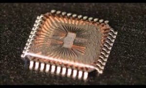
Break Microcontroller TI MSP430F448 can help engineer to disable the protective mechanism of MCU MSP430F448, the firmware in the flash memory can be readout directly with universal programmer
Low Supply-Voltage Range, 1.8 V to 3.6 V
Ultralow-Power Consumption:
– Active Mode: 280 µA at 1 MHz, 2.2 V
– Standby Mode: 1.1 µA
– Off Mode (RAM Retention): 0.1 µA
Five Power Saving Modes
Wake-Up From Standby Mode in 6 µs 16-Bit RISC Architecture,
125-ns Instruction Cycle Time
12-Bit A/D Converter With Internal
Reference, Sample-and-Hold and Autoscan
Feature
16-Bit Timer With Three† or Seven‡
Capture/Compare-With-Shadow Registers, Timer_B Serial Onboard Programming,
No External Programming Voltage Needed Programmable Code Protection by Security Fuse
Integrated LCD Driver for Up to 160 Segments
Family Members Include:
– MSP430F435:
16KB+256B Flash Memory,
512B RAM
– MSP430F436:
24KB+256B Flash Memory,
1KB RAM
– MSP430F437:
32KB+256B Flash Memory,
1KB RAM
16-Bit Timer With Three Capture/Compare Registers, Timer_A On-Chip Comparator Serial Communication Interface (USART), Select Asynchronous UART or Synchronous SPI by Software;
Two USARTs (USART0, USART1) In MSP430x44x Devices One USART (USART0) In MSP430x43x
Devices Brownout Detector Supply Voltage Supervisor/Monitor With Programmable Level Detection
– MSP430F447:
32KB+256B Flash Memory,
1KB RAM
– MSP430F448:
48KB+256B Flash Memory,
2KB RAM
– MSP430F449:
60KB+256B Flash Memory,
2KB RAM
For Complete Module Descriptions, See The MSP430x4xx Family User’s Guide
Literature Number SLAU056 ’F435, ’F436, and ’F437 devices ’F447, ’F448, and ’F449 devices
description
The Texas Instruments MSP430 series is an ultralow-power microcontroller family consisting of several devices featuring different sets of modules targeted to various applications. The microcontroller is designed to be battery operated for use in extended-time applications.
The MSP430 achieves maximum code efficiency with its 16-bit RISC architecture, 16-bit CPU-integrated registers, and a constant generator. The digitally-controlled oscillator provides wake-up from low-power mode to active mode in less than 6 µs.
The MSP430x43x and the MSP430x44x series are microcontroller configurations with two built-in 16-bit timers, a fast 12-bit A/D converter, one or two universal serial synchronous/asynchronous communication interfaces (USART), 48 I/O pins, and a liquid crystal driver (LCD) with up to 160 segments.
![A TI MSP430F448 mikrovezérlő egy alacsony teljesítményű, nagy teljesítményű chip, amelyet általában ipari, orvosi és autóipari alkalmazásokban használnak. Beágyazott flash memória, EEPROM és rögzített firmware -védelemmel rendelkezik az illetéktelen hozzáférés megakadályozása érdekében. Vannak azonban olyan esetek, amikor a felhasználóknak vissza kell állítaniuk, másolni vagy klónozniuk kell a firmware -t - akár biztonsági másolatot, hibakeresést, rendszer migrációját vagy fordított tervezését. A [Az Ön cégneve] oldalán a Mikrovezérlő TI MSP430F448 firmware törésére szakosodunk, segítve az ügyfelek dekódolását, dekódolását és a védett adatok feloldását az elemzéshez és a módosításhoz.](https://www.ic-crack.com/wp-content/uploads/2014/03/1.png)
A TI MSP430F448 mikrovezérlő egy alacsony teljesítményű, nagy teljesítményű chip, amelyet általában ipari, orvosi és autóipari alkalmazásokban használnak. Beágyazott flash memória, EEPROM és rögzített firmware -védelemmel rendelkezik az illetéktelen hozzáférés megakadályozása érdekében. Vannak azonban olyan esetek, amikor a felhasználóknak vissza kell állítaniuk, másolni vagy klónozniuk kell a firmware -t – akár biztonsági másolatot, hibakeresést, rendszer migrációját vagy fordított tervezését. A [Az Ön cégneve] oldalán a Mikrovezérlő TI MSP430F448 firmware törésére szakosodunk, segítve az ügyfelek dekódolását, dekódolását és a védett adatok feloldását az elemzéshez és a módosításhoz.
The TI MSP430F448 microcontroller is a low-power, high-performance chip commonly used in industrial, medical, and automotive applications. It features embedded flash memory, EEPROM, and secured firmware protection to prevent unauthorized access. However, there are cases where users need to restore, copy, or clone the firmware—whether for backup, debugging, system migration, or reverse engineering. At [Your Company Name], we specialize in breaking the microcontroller TI MSP430F448 firmware, helping clients decode, decrypt, and unlock protected data for analysis and modification.
Procedures to Crack TI MSP430F448 Firmware Protection
![Микроконтроллер TI MSP430F448 представляет собой высокопроизводительный чип, обычно используемый в промышленных, медицинских и автомобильных приложениях. Он оснащен встроенной флэш -памятью, EEPROM и защитой прошивки для предотвращения несанкционированного доступа. Тем не менее, есть случаи, когда пользователям необходимо восстановить, копировать или клонировать прошивку - будь то для резервного копирования, отладки, миграции системы или обратной инженерии. В [название вашей компании] мы специализируемся на нарушении прошивки микроконтроллера TI MSP430F448, помогая клиентам декодировать, расшифровать и разблокировать защищенные данные для анализа и модификации.](https://www.ic-crack.com/wp-content/uploads/2014/03/2.png)
Микроконтроллер TI MSP430F448 представляет собой высокопроизводительный чип, обычно используемый в промышленных, медицинских и автомобильных приложениях. Он оснащен встроенной флэш -памятью, EEPROM и защитой прошивки для предотвращения несанкционированного доступа. Тем не менее, есть случаи, когда пользователям необходимо восстановить, копировать или клонировать прошивку – будь то для резервного копирования, отладки, миграции системы или обратной инженерии. В [название вашей компании] мы специализируемся на нарушении прошивки микроконтроллера TI MSP430F448, помогая клиентам декодировать, расшифровать и разблокировать защищенные данные для анализа и модификации.
-
Firmware Extraction – We use advanced hardware tools to read and copy the flash and EEPROM memory, even when the firmware is protected or encrypted. Our techniques allow us to bypass security restrictions and gain access to the heximal or binary data stored in the microcontroller.
-
Disassembly and Reverse Engineering – After extracting the firmware, we decode and disassemble the locked program into machine-readable instructions. This process helps restore the embedded source code and allows deeper analysis of system behavior.
-
Decryption and Source Code Reconstruction – If the firmware is encrypted, we apply specialized algorithms to decrypt and reconstruct the original program. Our goal is to unlock the protected data archive and convert it into a readable and modifiable format.
-
Cloning and Duplication – Once the firmware is extracted and decrypted, we assist in duplicating or cloning the embedded program, making it transferable to other microcontrollers or systems. This step is crucial for system upgrades, debugging, and functional replication.
Why Choose Our TI MSP430F448 Hacking Service?
Stručnost u sigurnosnom zaobilaženju Microcontroller – Naš tim ima veliko iskustvo u pucanju zaključanog firmvera i dešifriranju osiguranih memorijskih datoteka.
Napredne tehnike dešifriranja – koristimo najnovije alati za hakiranje firmvera i obrnuti inženjering kako bismo osigurali točno i učinkovito vađenje podataka.
Stroga povjerljivost – Svi projekti upravljaju se s potpunom sigurnošću i povjerljivošću, osiguravajući integritet podataka i privatnost.
-
Expertise in Microcontroller Security Bypass – Our team has extensive experience in cracking locked firmware and decrypting secured memory files.
-
Advanced Decryption Techniques – We use the latest firmware hacking and reverse engineering tools to ensure accurate and efficient data extraction.
-
Strict Confidentiality – All projects are handled with full security and confidentiality, ensuring data integrity and privacy.
If you need to break, unlock, or copy the protected firmware of the TI MSP430F448 microcontroller, contact us today. Our professional reverse engineering solutions will help you restore and duplicate secured software with precision and reliability.
Posted in Break IC |
Tags: break microcontroller binary file, break microcontroller dump information, break microcontroller embedded firmware, break microcontroller encrypt program, break microcontroller flash content, break microcontroller heximal data, break microcontroller locked archive, break microcontroller protect eeprom, break microcontroller software memory, break microcontroller source code |
Comments Closed
Break IC Renesas R5F2L388CNFP Firmware
Break IC Renesas R5F2L388CNFP protection, decapsulate the silicon package of Microcontroller R5F2L388CNFP and readout firmware from MCU R5F2L388CNFP data memory and code memory, then make R5F2L388CNFP MCU clone units through this firmware;
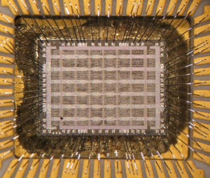
Break IC Renesas R5F2L388CNFP protection, decapsulate the silicon package of Microcontroller R5F2L388CNFP and readout firmware from MCU R5F2L388CNFP data memory and code memory, then make R5F2L388CNFP MCU clone units through this firmware
Features
The R8C/L35C Group, R8C/L36C Group, R8C/L38C Group, and R8C/L3AC Group of single-chip MCUs when incorporate the R8C CPU core, which implements a powerful instruction set for a high level of efficiency and supports a 1 Mbyte address space, allowing execution of instructions at high speed. In addition, the CPU core integrates a multiplier for high-speed operation processing.
Power consumption is low, and the supported operating modes allow additional power control. These MCUs are designed to maximize EMI/EMS performance.
Integration of many peripheral functions, including multifunction timer and serial interface, helps reduce the number of system components.
These groups have data flash (1 KB × 4 blocks) with the background operation (BGO) function.
Specification
CPU
Central processing unit R8C CPU core for the purpose of IC break
· Number of fundamental instructions: 89
· Minimum instruction execution time:
50 ns (f(XIN) = 20 MHz, VCC = 2.7 to 5.5 V)
200 ns (f(XIN) = 5 MHz, VCC = 1.8 to 5.5 V)
· Multiplier: 16 bits × 16 bits → 32 bits
· Multiply-accumulate instruction: 16 bits × 16 bits + 32 bits → 32 bits
· Operating mode: Single-chip mode (address space: 1 Mbyte)
Memory ROM/RAM
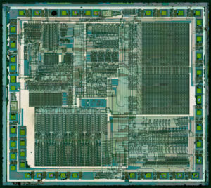
Break IC Renesas R5F2L388CNFP Firmware
Data flash
Refer to Tables 1.7 to 1.10 Product Lists.
Power Voltage detection circuit
Supply
Voltage
Detection
· Power-on reset
· Voltage detection 3 (detection level of voltage detection 0 and voltage detection 1 selectable)
I/O Ports Programmable
I/O ports
R8C/L35C Group
· CMOS I/O ports: 41, selectable pull-up resistor
· High current drive ports: 5
R8C/L36C Group
· CMOS I/O ports: 52, selectable pull-up resistor
· High current drive ports: 8
R8C/L38C Group
· CMOS I/O ports: 68, selectable pull-up resistor
· High current drive ports: 8 R8C/L3AC Group
· CMOS I/O ports: 88, selectable pull-up resistor
· High current drive ports: 16 Clock Clock generation circuits
4 circuits: XIN clock oscillation circuit
XCIN clock oscillation circuit (32 kHz)
High-speed on-chip oscillator (with frequency adjustment function)
Low-speed on-chip oscillator
· Oscillation stop detection:
XIN clock oscillation stop detection function
· Frequency divider circuit:
Division ratio selectable from 1, 2, 4, 8, and 16
· Low-power-consumption modes:
Standard operating mode (high-speed clock, low-speed clock, high-
speed on-chip oscillator, low-speed on-chip oscillator), wait mode,
stop mode, power-off mode
Real-time clock (timer RE)
Interrupts
R8C/L35C Group
· Number of interrupt vectors: 69
· External Interrupt: 9 (INT × 5, key input × 4)
· Priority levels: 7 levels
R8C/L36C Group
· Number of interrupt vectors: 69
· External Interrupt: 12 (INT × 8, key input × 4)
· Priority levels: 7 levels
R8C/L38C Group
· Number of interrupt vectors: 69
· External Interrupt: 16 (INT × 8, key input × 8)
· Priority levels: 7 levels
R8C/L3AC Group
· Number of interrupt vectors: 69
· External Interrupt: 16 (INT × 8, key input × 8)
· Priority levels: 7 levels
Watchdog Timer
· 14 bits × 1 (with prescaler)
· Selectable reset start function
· Selectable low-speed on-chip oscillator for watchdog timer
DTC (Data Transfer Controller)
· 1 channel
· Activation sources: 38
· Transfer modes: 2 (normal mode, repeat mode)
· Transfer modes: 2 (normal mode, repeat mode)
Reverse LATTICE CPLD Source code
Reverse LATTICE CPLD source code is a process to extract jed file from encrypted Lattice CPLD, using physical MCU invasive cracking method include decapsulation and focus ion beam can help to fulfill the task;
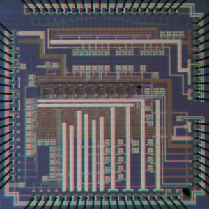
Reverse LATTICE CPLD source code is a process to extract jed file from encrypted Lattice CPLD, using physical MCU invasive cracking method include decapsulation and focus ion beam can help to fulfill the task
The same memory type but built with newer technologies such as 0.9 µm in the Microchip PIC16CR57 microcontroller [124] and 1.0 µm in the Motorola MC68HC705C9A microcontroller [23] requires deprocessing because the top bit-line metal wires obstruct observation of the transistors.
NAND Mask ROM memory type with metal layer programming was used in the NEC µPD78F9116 microcontroller [125] fabricated with 0.35 µm technology. As all the internal layers were planarised, deeper layers cannot be observed unless the top metal layer is removed.
This was accomplished by using Nitrox etching for the passivation layer followed by treatment in a 33% water solution of KOH to etch the top aluminium metal layer but preserving the interconnection layer which is probably made out of tungsten (because when the HCl solution was used to etch the top metal layer, the interconnection layer was etched away as well).
Posted in Break IC |
Tags: extract fpga ic binary file, extract fpga ic dump information, extract fpga ic embedded firmware, extract fpga ic encrypt program, extract fpga ic flash content, extract fpga ic heximal data, extract fpga ic locked archive, extract fpga ic protect eeprom, extract fpga ic software memory, extract fpga ic source code |
Comments Closed
Reverse DSP CPLD IC Chip Program
Reverse DSP CPLD IC Chip Program from memory, and copy memory content to new CPLD chip which will provide the same functions as original DSP chip by Crack CPLD protection.
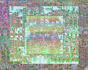
Reverse DSP CPLD IC Chip Program from memory, and copy memory content to new CPLD chip which will provide the same functions as original DSP chip by Crack CPLD protection
Layout reconstruction requires the images of all the layers inside the chip to be combined. The images are normally taken automatically using a motorised stage to move the sample and special software to combine all the images together.
Normally, for semiconductor chips fabricated with 0.13 µm or smaller technology, images are created using a SEM which has a resolution better than 10 nm.
Posted in Break IC |
Tags: extract avr microcontroller binary file, extract avr microcontroller dump information, extract avr microcontroller embedded firmware, extract avr microcontroller encrypt program, extract avr microcontroller flash content, extract avr microcontroller heximal data, extract avr microcontroller locked archive, extract avr microcontroller protect eeprom, extract avr microcontroller software memory, extract avr microcontroller source code |
Comments Closed
Read Lattice CPLD embeded firmware
Read Lattice CPLD embeded firmware from locked memory, the file format of CPLD can be JED, unlock CPLD tamper resistance system by cut off the security fuse.
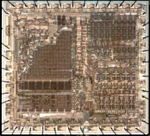
Read Lattice CPLD embeded firmware from locked memory, the file format of CPLD can be JED, unlock CPLD tamper resistance system by cut off the security fuse
The main disadvantage of high resolution microscopes is the short working distance between the objective and a specimen, especially at high magnifications (about 0.3 mm with 100× objective). As a result partially decapsulated chips cannot be observed and full decapsulation of the die is required. Using microscopes with a long working distance, for example the Mitutoyo FS70 [121] with 13 mm working distance on 200× objective, helps solve this problem but at a cost: the resolution is at most 0.4 µm because the NA cannot be high.
Another problem of the high-resolution objectives is a very short depth of focus, which makes the out-of-focus planes look blurred, thus reducing the image quality. This is more noticeable on multilayer chips where the distance between the top and the bottom layer is more than 1 µm.
Confocal microscopy reduces this effect as all out-of-focus planes become dark or appear in different colours depending from their depth. Such confocal systems are very expensive, especially the ones that use laser scanning, and therefore can be afforded by relatively large labs only. Even second-hand confocal microscopes start from £10,000.
Posted in Break IC |
Tags: extract atmel microcontroller binary file, extract atmel microcontroller dump information, extract atmel microcontroller embedded firmware, extract atmel microcontroller encrypt program, extract atmel microcontroller flash content, extract atmel microcontroller heximal data, extract atmel microcontroller locked archive, extract atmel microcontroller protect eeprom, extract atmel microcontroller software memory, extract atmel microcontroller source code |
Comments Closed
Copy Encrypted Microchip PIC18F2330 Heximal
Copy Encrypted Microchip PIC18F2330 Heximal
The Flash Program Memory and firmware data memory are organized in pages which can be Copy Encrypted Microchip PIC18F2330 Heximal. The pages are word accessible for the Flash and byte accessible for the firmware. Table 7-2 on page 14 shows the Flash Program Memory organization.
Flash write and erase operations are performed on one page at a time, while reading the Flash is done one byte at a time. For Flash access the Z-pointer (Z[m:n]) is used for addressing. The most significant bits in the address (FPAGE) gives the page number and the least significant address bits (FWORD) gives the word.
Table 7-3 on page 14 shows firmware memory organization for the PIC18F2320 devices. Efirmware write and erase operations can be performed one page or one byte at a time, while reading the firmware is done one byte at a time.
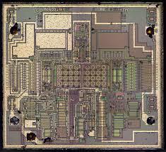
Copy Encrypted Microchip PIC18F2330 Heximal
For firmware access the NVM Address Register (ADDR[m:n]) is used for addressing. The most significant bits in the address (E2PAGE) gives the page number and the least significant address bits (E2BYTE) gives the byte.
The PIC18F2320 has a Direct Memory Access (DMA) Controller to move data between memories and peripherals in the data space. The DMA controller uses the same data bus as the CPU to transfer data. It has 4 channels that can be configured independently. Each DMA channel can perform data transfers in blocks of configurable size from 1 to 64K bytes.
A repeat counter can be used to repeat each block transfer for single transactions up to 16M bytes. Each DMA channel can be configured to access the source and destination memory address with incrementing, decrementing or static addressing. The addressing is independent for source and destination address.
When the transaction is complete the original source and destination address can automatically be reloaded to be ready for the next transaction. The DMAC can access all the peripherals through their I/O memory registers, and the DMA may be used for automatic transfer of data to/from communication modules, as well as automatic data retrieval from ADC conversions, data transfer to DAC conversions, or data transfer to or from port pins.
A wide range of transfer triggers is available from the peripherals, Event System and software. Each DMA channel has different transfer triggers. To allow for continuous transfers, two channels can be interlinked so that the second takes over the transfer when the first is finished and vice versa. The DMA controller can read from memory mapped firmware, but it cannot write to the firmware or access the Flash before CRACK MCU.
Read DSP CPLD Dump information
Read DSP CPLD Dump information from CPLD storage memory, unlock CPLD memory through CPLD cracking method, mostly from invasive method which will involve reverse engineering CPLD physical hardware and get access to the security fuse bit;
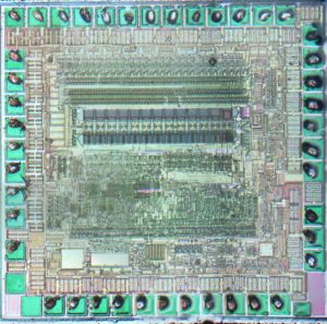
Read DSP CPLD Dump information from CPLD storage memory, unlock CPLD memory through CPLD cracking method, mostly from invasive method which will involve reverse engineering CPLD physical hardware and get access to the security fuse bit
In practice the maximum resolution which can be achieved with a standard 100× objective (NA = 0.9) is about 0.3 µm. In order to obtain higher working NA the refractive index of the medium between the objective and the specimen must be increased. There are objectives that allow imaging in water (n = 1.33) and immersion oil (n = 1.51). That increases the maximum resolution up to 0.2 µm for 100× objective. Another way of increasing the resolution is using a shorter wavelength. By shifting to near-ultraviolet (NUV) light with 360 nm wavelength, the resolution can be increased to 0.18 µm, but this requires special CCD cameras.
Some microscopes have additional features aimed at increasing the contrast of the image and thereby achieving the highest possible resolution. These are darkfield (DF) illumination, differential interference contrast [114], phase contrast [115] and confocal imaging [116]. All the major microscope manufacturers such as Nikon, Olympus, Carl Zeiss and Leica offer a wide range of models from basic to high-end; the latter have all the features necessary to achieve the highest resolution. There are models specifically designed for semiconductor analysis such as the Nikon Optiphot 200C [117], Olympus MX50 [118], Zeiss Axiotron 2 [119] and Leica INM100 [120].
Posted in Break IC |
Tags: extract lattice ic binary file, extract lattice ic dump information, extract lattice ic embedded firmware, extract lattice ic encrypt program, extract lattice ic flash content, extract lattice ic heximal content, extract lattice ic locked archive, extract lattice ic protect eeprom, extract lattice ic software memory, extract lattice ic source code |
Comments Closed
Crack PIC16F716 MCU Source Code
Crack PIC16F716 MCU Source Code
Crack PIC16F716 MCU Source Code means the source code will be readout from its memory after the PIC16F716 protection has been disabled:
Microcontroller Core Features:
· High-performance RISC CPU
· Only 35 single-word instructions to learn
– All single-cycle instructions except for program branches which are two-cycle
· Operating speed: DC – 20 MHz clock input DC – 200 ns instruction cycle
· Interrupt capability (up to 7 internal/external interrupt sources)
· 8-level deep hardware stack
· Direct, Indirect and Relative Addressing modes
Special Microcontroller Features:
· Power-on Reset (POR)
· Power-up Timer (PWRT) and
Oscillator Start-up Timer (OST)
· Watchdog Timer (WDT) with its own on-chip RC oscillator for reliable operation
· Dual level Brown-out Reset circuitry
– 2.5 VBOR (Typical)
– 4.0 VBOR (Typical)
· Programmable code protection
· Power-Saving Sleep mode
· Selectable oscillator options
· Fully static design
· In-Circuit Serial Programming (ICSP™) CMOS Technology:

Crack PIC16F716 MCU Source Code
· Wide operating voltage range:
– Industrial: 2.0V to 5.5V
– Extended: 3.0V to 5.5V
· High Sink/Source Current 25/25 mA
· Wide temperature range:
– Industrial: -40°C to 85°C
– Extended: -40°C to 125°C
Low-Power Features:
· Standby Current:
– 100 nA @ 2.0V, typical
· Operating Current:
– 14 ìA @ 32 kHz, 2.0V, typical
– 120 ìA @ 1 MHz, 2.0V, typical
· Watchdog Timer Circuit:
– 1 ìA @ 2.0V, typical
· Timer1 Oscillator Current:
– 3.0 ìA @ 32 kHz, 2.0V, typical
Peripheral Features:
· Timer0: 8-bit timer/counter with 8-bit prescaler
· Timer1: 16-bit timer/counter with prescaler can be incremented during Sleep via external crystal/clock
· Timer2: 8-bit timer/counter with 8-bit period register, prescaler and postscaler
· Enhanced Capture, Compare, PWM module:
– Capture is 16-bit, max. resolution is 12.5 ns
– Compare is 16-bit, max. resolution is 200 ns
– PWM maximum resolution is 10-bit
– Enhanced PWM:
– Single, Half-Bridge and Full-Bridge modes
– Digitally programmable dead-band delay
– Auto-shutdown/restart
· 8-bit multi-channel Analog-to-Digital Converter
· 13 I/O pins with individual direction control
· Programmable weak pull-ups on PORTB