Archive for the ‘Break IC’ Category
 Break IC ATmega32A Software
 June 18th, 2015 |
  Author:
 Breaking IC ATmega32A software involves cracking or decoding the secured and encrypted firmware stored in the microcontroller’s flash memory and EEPROM memory. The ATmega32A MCU, like many modern microprocessors, is designed with protective measures to prevent unauthorized access to its program, binary, and source code. To unlock and restore this software, reverse engineering techniques are often employed.
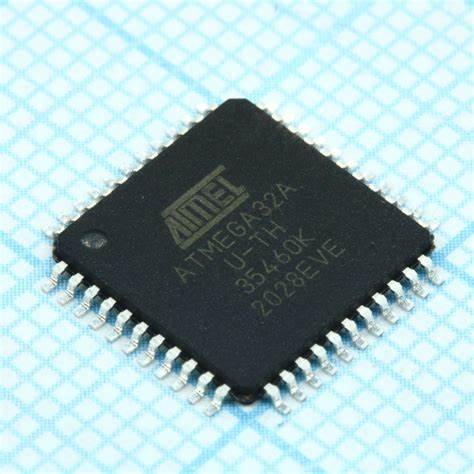
breaking IC ATmega32A software involves cracking or decoding the secured and encrypted firmware stored in the ATmega32A microcontroller’s flash memory and EEPROM memory. The ATmega32A MCU, like many modern microprocessors, is designed with protective measures to prevent unauthorized access to its program, binary, and source code. To unlock and restore this software, reverse engineering techniques are often employed
The first step in breaking the IC’s software is to analyze the microprocessor’s architecture and security features. These security mechanisms, which may include encryption or lockouts, are intended to protect the integrity of the firmware. Once these protective layers are bypassed, the embedded program can be extracted from the flash memory and EEPROM memory. The extracted binary or heximal data is then decoded to retrieve the source code, which can be restored, cloned, or replicated for use in different applications.
Unlocking the ATmega32A software also opens the door to cloning the firmware for use in other devices or systems. This process ensures that the program can be duplicated for backup purposes or hardware replication. Additionally, breaking the software can allow for troubleshooting or upgrading the system, especially when original source code or design files are unavailable.
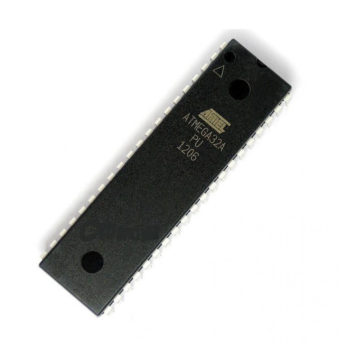
разбиване на IC Софтуерът ATmega32A включва кракване или декодиране на защитения и криптиран фърмуер, съхраняван във флаш паметта и EEPROM паметта на микроконтролера ATmega32A. ATmega32A MCU, подобно на много съвременни микропроцесори, е проектиран със защитни мерки за предотвратяване на неоторизиран достъп до неговата програма, двоичен и изходен код. За отключване и възстановяване на този софтуер често се използват техники за обратно инженерство
While breaking IC ATmega32A software can be a valuable technique for system recovery or hardware maintenance, it is essential to operate within legal and ethical boundaries. Unauthorized cracking, decoding, or cloning of software can violate intellectual property rights and lead to legal consequences. Proper authorization and adherence to intellectual property laws are essential when performing these activities.
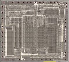
We can Break IC ATMEGA32A Software, please view the IC ATMEGA32A features for your reference:
In order to maximize performance and parallelism, the AVR uses a Harvard architecture – with separate memories and buses for program and data. Instructions in the program memory are executed with a single level pipelining. While one instruction is being executed, the next instruction is pre-fetched from the program memory. This concept enables instructions to be executed in every clock cycle. The program memory is In-System Reprogrammable Flash memory. The fast-access Register File contains 32 x 8-bit general purpose working registers with a single clock cycle access time. This allows single-cycle Arithmetic Logic Unit (ALU) operation. In a typical ALU operation, two operands are output from the Register File, the operation is executed, and the result is stored back in the Register File – in one clock cycle. Six of the 32 registers can be used as three 16-bit indirect address register pointers for Data Space addressing – enabling efficient address calculations before Break IC.
One of the these address pointers can also be used as an address pointer for look up tables in Flash Program memory. These added function registers are the 16-bit X-, Y-, and Z-register, described later in this section. The ALU supports arithmetic and logic operations between registers or between a constant and a register. Single register operations can also be executed in the ALU. After an arithmetic operation, the Status Register is updated to reflect information about the result of the operation. Program flow is provided by conditional and unconditional jump and call instructions, able to directly address the whole address space. Most AVR instructions have a single 16-bit word format when Break IC.
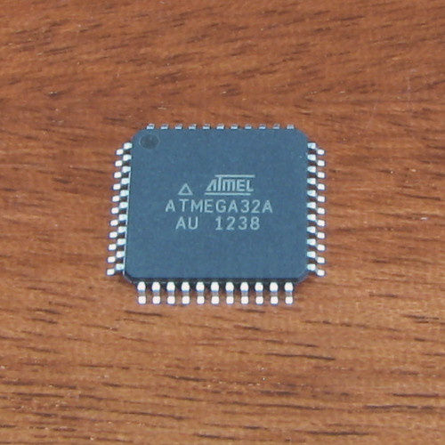
IC ATmega32A yazılımını kırmak, ATmega32A mikrodenetleyicisinin flaş belleğinde ve EEPROM belleğinde saklanan güvenli ve şifreli aygıt yazılımını kırmayı veya kodunu çözmeyi içerir. ATmega32A MCU, birçok modern mikroişlemci gibi, programına, ikili dosyasına ve kaynak koduna yetkisiz erişimi önlemek için koruyucu önlemlerle tasarlanmıştır. Bu yazılımın kilidini açmak ve geri yüklemek için genellikle tersine mühendislik teknikleri kullanılır
Every program memory address contains a 16- or 32-bit instruction. Program Flash memory space is divided in two sections, the Boot program section and the Application Program section. Both sections have dedicated Lock bits for write and break/write protection. The SPM instruction that writes into the Application Flash memory section must reside in the Boot Program section. During interrupts and subroutine calls, the return address Program Counter (PC) is stored on the Stack. The Stack is effectively allocated in the general data SRAM, and consequently the Stack size is only limited by the total SRAM size and the usage of the SRAM. All user programs must initialize the SP in the reset routine (before subroutines or interrupts are executed). The Stack Pointer SP is break/write accessible in the I/O space.
The data SRAM can easily be accessed through the five different addressing modes supported in the AVR architecture. The memory spaces in the AVR architecture are all linear and regular memory maps. A flexible interrupt module has its control registers in the I/O space with an additional global interrupt enable bit in the Status Register. All interrupts have a separate interrupt vector in the interrupt vector table after Break IC.
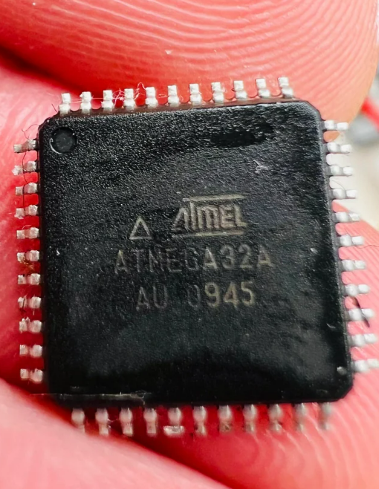
IC ATmega32A 소프트웨어를 깨는 것은 ATmega32A 마이크로컨트롤러의 플래시 메모리와 EEPROM 메모리에 저장된 보안되고 암호화된 펌웨어를 크래킹하거나 디코딩하는 것을 포함합니다. 많은 최신 마이크로프로세서와 마찬가지로 ATmega32A MCU는 프로그램, 바이너리 및 소스 코드에 대한 무단 액세스를 방지하기 위한 보호 조치로 설계되었습니다. 이 소프트웨어의 잠금을 해제하고 복원하기 위해 종종 역엔지니어링 기술이 사용됩니다.
The interrupts have priority in accordance with their interrupt vector position. The lower the interrupt vector address, the higher the priority. The I/O memory space contains 64 addresses for CPU peripheral functions as Control Registers, SPI, and other I/O functions. The I/O Memory can be accessed directly, or as the Data Space locations following those of the Register File, $20 – $5F.
 Posted in
Break MCU ATMEGA16PA Flash
Break MCU ATMEGA16PA Flash
We can Break MCU ATmega16PA Flash, please view the Mcu ATMEGA16PA features for your reference:
First Analog Comparator conversion may be delayed. If the device is powered by a slow rising VCC, the first Analog Comparator conversion will take longer than expected on some devices by Crack MCU.
Problem Fix/Workaround
When the device has been powered or reset, disable then enable theAnalog Comparator before the first conversion.
Interrupts may be lost when writing the timer registers in the asynchronous timer
The interrupt will be lost if a timer register that is synchronized to the asynchronous timer clock is written when the asynchronous Timer/Counter register(TCNTx) is 0x00 if Break MCU ATMEGA16PA Flash.
Problem Fix / Workaround
Always check that the asynchronous Timer/Counter register neither have the value 0xFF nor 0x00 before writing to the asynchronous Timer Control Register(TCCRx), asynchronous Timer Counter Register(TCNTx), or asynchronous Output Compare Register(OCRx).
IDCODE masks data from TDI input, The JTAG instruction IDCODE is not working correctly. Data to succeeding devices are replaced by all-ones during Update-DR in the process of Recover Chip PIC16F620A Binary.
Problem Fix / Workaround
If ATmega16 is the only device in the scan chain, the problem is not visible. Select the Device ID Register of the ATmega16 by issuing the IDCODE instruction or by entering the Test-Logic-Reset state of the TAP controller to break out the contents of its Device ID Register and possibly data from succeeding devices of the scan chain.
Issue the BYPASS instruction to the ATmega16 while breaking the Device ID Registers of preceding devices of the boundary scan chain. If the Device IDs of all devices in the boundary scan chain must be captured simultaneously, the ATmega16 must be the fist device in the chain to facilitate the progress of Recover Chip PIC16C621 Program.
Breaking EEPROM by using ST or STS to set EERE bit triggers unexpected interrupt request.
Breaking EEPROM by using the ST or STS command to set the EERE bit in the EECR register triggers an unexpected EEPROM interrupt request.
Problem Fix / Workaround
Always use OUT or SBI to set EERE in EECR.
First Analog Comparator conversion may be delayed
If the device is powered by a slow rising VCC, the first Analog Comparator conversion will take longer than expected on some devices.
Problem Fix/Workaround
When the device has been powered or reset, disable then enable theAnalog Comparator before the first conversion. Interrupts may be lost when writing the timer registers in the asynchronous timer, The interrupt will be lost if a timer register that is synchronized to the asynchronous timer clock is written when the asynchronous Timer/Counter register(TCNTx) is 0x00.
Problem Fix / Workaround
Always check that the asynchronous Timer/Counter register neither have the value 0xFF nor 0x00 before writing to the asynchronous Timer Control Register(TCCRx), asynchronous Timer Counter Register(TCNTx), or asynchronous Output Compare Register(OCRx).
IDCODE masks data from TDI input
The JTAG instruction IDCODE is not working correctly. Data to succeeding devices are replaced by all-ones during Update-DR.
Problem Fix / Workaround
If ATmega16 is the only device in the scan chain, the problem is not visible.
Select the Device ID Register of the ATmega16 by issuing the IDCODE instruction or by entering the Test-Logic-Reset state of the TAP controller to break out the contents of its Device ID Register and possibly data from succeeding devices of the scan chain. Issue the BYPASS instruction to the ATmega16 while breaking the Device ID.
Registers of preceding devices of the boundary scan chain. If the Device IDs of all devices in the boundary scan chain must be captured simultaneously by Reverse Engineering Microcontroller PIC16C620 Code, the ATmega16 must be the fist device in the chain.
Breaking EEPROM by using ST or STS to set EERE bit triggers unexpected interrupt request.
Breaking EEPROM by using the ST or STS command to set the EERE bit in the EECR register triggers an unexpected EEPROM interrupt request.
Problem Fix / Workaround
Always use OUT or SBI to set EERE in EECR.
Break IC TS80C58X2 Code
We can Break IC TS80C58X2 Code, please view the IC TS80C58X2 features for your reference:
Software can take advantage of the additional data pointers to both increase speed and reduce code size, for example, block operations (copy, compare, search …) are well served by using one data pointer as a ’source’ pointer and the other one as a “destination” pointer.
INC is a short (2 bytes) and fast (12 clocks) way to manipulate the DPS bit in the AUXR1 SFR. However, note that the INC instruction does not directly force the DPS bit to a particular state, but simply toggles it.
In simple routines, such as the block move example, only the fact that DPS is toggled in the proper sequence matters, not its actual value. In other words, the block move routine works the same whether DPS is ‘0’ or ‘1’ on entry. Observe that without the last instruction (INC AUXR1), the routine will exit with DPS in the opposite state.
The timer 2 in the TS80C54/58X2 is compatible with the timer 2 in the 80C52. It is a 16-bit timer/counter: the count is maintained by two eight-bit timer registers, TH2 and TL2, connected in cascade. It is controlled by T2CON register (See Table 6) and T2MOD register (See Table 7) after Break IC TS80C58X2 Code.
Timer 2 operation is similar to Timer 0 and Timer 1. C/T2 selects FOSC/12 (timer operation) or external pin T2 (counter operation) as the timer clock input. Setting TR2 allows TL2 to be incremented by the selected input.
Timer 2 has 3 operating modes: capture, autoreload and Baud Rate Generator. These modes are selected by the combination of RCLK, TCLK and CP/RL2 (T2CON), as described in the Atmel Wireless & Microcontrollers 8-bit Microcontroller Hardware description.
Refer to the Atmel Wireless & Microcontrollers 8-bit Microcontroller Hardware description for the description of Capture and Baud Rate Generator Modes. In TS80C54/58X2 Timer 2 includes the following enhancements:
Auto-reload mode with up or down counter
Programmable clock-output
The auto-reload mode configures timer 2 as a 16-bit timer or event counter with automatic reload. If DCEN bit in T2MOD is cleared, timer 2 behaves as in 80C52 (refer to the Atmel Wireless & Microcontrollers 8-bit Microcontroller Hardware description). If DCEN bit is set, timer 2 acts as an Up/down timer/counter as shown in Figure 4. In this mode the T2EX pin controls the direction of count.
Break IC TS80C58X2 Code
When T2EX is high, timer 2 counts up. Timer overflow occurs at FFFFh which sets the TF2 flag and generates an interrupt request. The overflow also causes the 16-bit value in RCAP2H and RCAP2L registers to be loaded into the timer registers TH2 and TL2.
When T2EX is low, timer 2 counts down. Timer underflow occurs when the count in the timer registers TH2 and TL2 equals the value stored in RCAP2H and RCAP2L registers. The underflow sets TF2 flag and reloads FFFFh into the timer registers.
The EXF2 bit toggles when timer 2 overflows or underflows according to the the direction of the count. EXF2 does not generate any interrupt. This bit can be used to provide 17-bit resolution.
Break IC TS83C51U2 Heximal
Break IC TS83C51U2 Heximal
We can Break IC TS83C51U2 Heximal, please view the IC TS83C51U2 features for your reference:
In this document, UART_0 will make reference to the first UART (present in all Atmel Wireless & Microcontrollers C51 derivatives) and UART_1 will make reference to the second UART, only present in the TS80C51U2 part.
The second UART (UART_1) can be seen as an alternate function of Port 1 (P1.2 or P1.6 for RXD1 and P1.3 or P1.7 for TXD1) or can be connected to (pin6 or pin12) and (pin28 or pin34) of 44-pin package (see Pin configuration). UART_1 is fully compliant with the first one allowing an internal baud rate generator to be the clock source.
This common internal baud rate generator can be used independently by each UART or both as clock source allowing to program various speeds.
The TS80C51U2 provides 7 sources of interrupt with four priority levels. UART_1 has a lower priority than Timer
The Serial Ports are full duplex meaning they can transmit and receive simultaneously. They are also receive buffered, meaning they can start reception of a second byte before a previously received byte has been break from the receive register from Break IC TS83C51U2 Heximal.
The Serial Port receive and transmit registers of UART_1 are both accessed at Special Function Register SBUF_1. Writing to SBUF_1 loads the transmit register and breaking SBUF_1 accesses a physical separate receive register.
Break IC TS83C51U2 Heximal
The UART_1 port control and status is the Special Function Register SCON_1. This register contains not only the mode selection bit but also the 9th bit for transmit and receive (TB8_1 and RB8_1) and the serial port interrupt bits (TI_1 and RI_1).
The automatic address recognition feature is enabled when multiprocessor communication is enabled. Implemented in hardware, automatic address recognition enhances the multiprocessor communication feature by allowing the Serial Port to examine address of each incoming frame and provides filtering capability after Break IC TS83C51U2 Heximal.
The UART_1 also comes with Frame error detection, similar to the UART_0. The Special Function Registers (SFRs) of the TS80C51U2 fall into the following categories:
C51 core registers: ACC, B, DPH, DPL, PSW, SP, AUXR1
I/O port registers: P0, P1, P2, P3 after Break IC
Timer registers: T2CON, T2MOD, TCON, TH0, TH1, TH2, TMOD, TL0, TL1, TL2, RCAP2L, RCAP2H
Serial I/O port registers for UART_0: SADDR_0, SADEN_0, SBUF_0, SCON_0
Serial I/O port registers for UART_1: SADDR_1, SADEN_1, SBUF_1, SCON_1
Baud Rate Generator registers: BRL, BDRCON, BDRCON_1
Power and clock control registers: PCON
HDW Watchdog Timer Reset: WDTRST, WDTPRG
Interrupt system registers: IE, IP, IPH
Others: AUXR, CKCONIn comparison to the original 80C52, the TS80C51U2 implements some new features, which are:
The X2 option
The second full duplex enhanced UART.
The Baud Rate generator.
The Dual Data Pointer.
The Watchdog.
The 4 level interrupt priority system.
The power-off flag.
The ONCE mode.
The ALE disabling.
Some enhanced features are also located in the UARTs and the timer 2
Break IC TS83C51U2 Binary
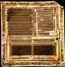
We can Break IC TS83C51U2 Binary, please view the IC TS83C51U2 features for your reference:
In this document, UART_0 will make reference to the first UART (present in all Atmel Wireless & Microcontrollers C51 derivatives) and UART_1 will make reference to the second UART, only present in the TS80C51U2 part. The second UART (UART_1) can be seen as an alternate function of Port 1 (P1.2 or P1.6 for RXD1 and P1.3 or P1.7 for TXD1) or can be connected to (pin6 or pin12) and (pin28 or pin34) of 44-pin package (see Pin configuration). UART_1 is fully compliant with the first one allowing an internal baud rate generator to be the clock source if Break IC.
This common internal baud rate generator can be used independently by each UART or both as clock source allowing to program various speeds.The TS80C51U2 provides 7 sources of interrupt with four priority levels. UART_1 has a lower priority than Timer, The Serial Ports are full duplex meaning they can transmit and receive simultaneously.
They are also receive buffered, meaning they can start reception of a second byte before a previously received byte has been break from the receive register.
The Serial Port receive and transmit registers of UART_1 are both accessed at Special Function Register SBUF_1. Writing to SBUF_1 loads the transmit register and breaking SBUF_1 accesses a physical separate receive register.
The UART_1 port control and status is the Special Function Register SCON_1. This register contains not only the mode selection bit but also the 9th bit for transmit and receive (TB8_1 and RB8_1) and the serial port interrupt bits (TI_1 and RI_1) before Break IC TS83C51U2 Binary.
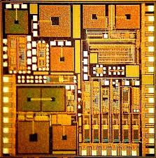
Break IC TS83C51U2 Binary
The automatic address recognition feature is enabled when multiprocessor communication is enabled. Implemented in hardware, automatic address recognition enhances the multiprocessor communication feature by allowing the Serial Port to examine address of each incoming frame and provides filtering capability.
The UART_1 also comes with Frame error detection, similar to the UART_0. The Special Function Registers (SFRs) of the TS80C51U2 fall into the following categories:
C51 core registers: ACC, B, DPH, DPL, PSW, SP, AUXR1
I/O port registers: P0, P1, P2, P3 after Break IC
Timer registers: T2CON, T2MOD, TCON, TH0, TH1, TH2, TMOD, TL0, TL1, TL2, RCAP2L, RCAP2H
Serial I/O port registers for UART_0: SADDR_0, SADEN_0, SBUF_0, SCON_0
Serial I/O port registers for UART_1: SADDR_1, SADEN_1, SBUF_1, SCON_1
Baud Rate Generator registers: BRL, BDRCON, BDRCON_1
Power and clock control registers: PCON
HDW Watchdog Timer Reset: WDTRST, WDTPRG
Interrupt system registers: IE, IP, IPH
Others: AUXR, CKCONIn comparison to the original 80C52, the TS80C51U2 implements some new features, which are:
The X2 option
The second full duplex enhanced UART.
The Baud Rate generator.
The Dual Data Pointer.
The Watchdog.
The 4 level interrupt priority system.
The power-off flag.
The ONCE mode.
The ALE disabling.
Some enhanced features are also located in the UARTs and the timer 2.
Break MCU PIC12CE674 Software
The high performance of the PIC12CE67X family can be attributed to a number of architectural features commonly found in RISC microprocessors which is critical part for Break MCU PIC12CE674 Software. To begin with, the PIC12CE67X uses a Harvard architecture, in which program and data are accessed from separate memories using separate buses.
This improves bandwidth over traditional von Neumann architecture in which program and data are fetched from the same memory using the same bus. Separating program and data buses also allow instructions to be sized differently than the 8-bit wide data word. Instruction opcodes are 14-bits wide making it possible to have all single word instructions.
A 14-bit wide program memory access bus fetches a 14-bit instruction in a single instruction cycle. A two-stage pipeline overlaps fetch and execution of instructions to facilitate the process of Copy MCU PIC18F4685 Software. Consequently, all instructions (35) execute in a single cycle (400 ns @ 10 MHz) except for program branches.
The table below lists program memory (EPROM), data memory (RAM), and non-volatile memory (EEPROM) for each PIC12C67X device. The PIC12C67X can directly or indirectly address its register files or data memory. All special function registers, including the program counter, are mapped in the data memory after Break MCU PIC12CE674 Software.
The PIC12C67X has an orthogonal (symmetrical) instruction set that makes it possible to carry out any operation on any register using any addressing mode to Crack MCU. This symmetrical nature and lack of ‘special optimal situations’ make programming with the PIC12C67X simple yet efficient.
In addition, the learning curve is reduced significantly. PIC12C67X devices contain an 8-bit ALU and working register. The ALU is a general purpose arithmetic unit. It performs arithmetic and Boolean functions between the data in the working register and any register file.
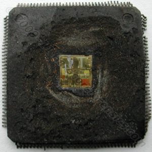
Break MCU PIC12CE674 Software
The ALU is 8-bits wide and capable of addition, subtraction, shift and logical operations. Unless otherwise mentioned, arithmetic operations are two’s complement in nature. In two-operand instructions, typically one operand is the working register (W register).
The other operand is a file register or an immediate constant. In single operand instructions, the operand is either the W register or a file register only after the completion of Recover IC PIC16F873 Heximal. The W register is an 8-bit working register used for ALU operations. It is not an addressable register.
Depending on the instruction executed, the ALU may affect the values of the Carry (C), Digit Carry (DC), and Zero (Z) bits in the STATUS register. The C and DC bits operate as a borrow bit and a digit borrow out bit, respectively, in subtraction. See the SUBLW and SUBWF instructions for examples.
Break Microcontroller PIC12C672 Heximal
The PIC12C67X devices are low-cost, high-performance, CMOS, fully-static, 8-bit microcontrollers with integrated analog-to-digital (A/D) converter and EEPROM data memory (EEPROM on PIC12CE67X versions only) when Break Microcontroller PIC12C672 Heximal.
All PICmicro® microcontrollers employ an advanced RISC architecture. The PIC12C67X microcontrollers have enhanced core features, eight-level deep stack, and multiple internal and external interrupt sources. The separate instruction and data buses of the Harvard architecture allow a 14-bit wide instruction word with the separate 8-bit wide data after IC Cloning. The two stage instruction pipeline allows all instructions to execute in a single cycle, except for program branches, which require two cycles.
Break Microcontroller PIC12C672 Heximal
A total of 35 instructions (reduced instruction set) are available. Additionally, a large register set gives some of the architectural innovations used to achieve a very high performance. PIC12C67X microcontrollers typically achieve a 2:1 code compression and a 4:1 speed improvement over other 8-bit microcontrollers in their class.
The PIC12C67X devices have 128 bytes of RAM, 16 bytes of EEPROM data memory (PIC12CE67X only), 5 I/O pins and 1 input pin. In addition a timer/counter is available. Also a 4-channel, high-speed, 8-bit A/D is provided. The 8-bit resolution is ideally suited for applications requiring low-cost analog interface which can be used for MC68HC05B6 microcontroller ic extract code, (i.e., thermostat control, pressure sensing, etc.) before Break MICROCONTROLLER
The PIC12C67X devices have special features to reduce external components, thus reducing cost, The PIC12C67X products are compatible with other members of the 14-bit PIC16CXXX families. enhancing system reliability and reducing power consumption.
The Power-On Reset (POR), Power-up Timer (PWRT), and Oscillator Start-up Timer (OST) eliminate the need for external reset circuitry. There are five oscillator configurations to choose from, including INTRC precision internal oscillator mode and the power-saving LP (Low Power) oscillator mode when Extract PIC16F84 MCU firmware. Power-saving SLEEP mode, Watchdog Timer and code protection features improve system cost, power and reliability.
The SLEEP (power-down) feature provides a power-saving mode. The user can wake-up the chip from SLEEP through several external and internal interrupts and resets when Break Microcontroller PIC12C672 Heximal.
Break IC PIC12C671 Eeprom
We can Break IC PIC12C671 Eeprom, please view the IC PIC12C671 features for your reference:
High-Performance RISC CPU:
· Only 35 single word instructions to learn
· All instructions are single cycle (400 ns) except for program branches which are two-cycle
· Operating speed: DC – 10 MHz clock input DC – 400 ns instruction cycle
· 14-bit wide instructions 8-bit wide data path
· Interrupt capability
· Special function hardware registers
· 8-level deep hardware stack
· Direct, indirect and relative addressing modes for data and instructions to facilitate the process of Extract PLD IC Firmware
Peripheral Features:
· Four-channel, 8-bit A/D converter
· 8-bit real time clock/counter (TMR0) with 8-bit programmable prescaler
· 1,000,000 erase/write cycle EEPROM data memory
· EEPROM data retention > 40 years
Special Microcontroller Features:
Break IC PIC12C671 Eeprom
In-Circuit Serial Programming (ICSP™)
Internal 4 MHz oscillator with programmable calibration
Selectable clockout
Power-on Reset (POR)
Power-up Timer (PWRT) and Oscillator Start-up Timer (OST)
Watchdog Timer (WDT) with its own on-chip RC oscillator for reliable operation in order to Extract PLD MCU code
Power saving SLEEP mode
Interrupt-on-pin change (GP0, GP1, GP3)
Internal pull-ups on I/O pins (GP0, GP1, GP3)
Internal pull-up on MCLR pin
Selectable oscillator options:
– INTRC: Precision internal 4 MHz oscillator
– EXTRC: External low-cost RC oscillator
– XT: Standard crystal/resonator
– HS: High speed crystal/resonator after Break IC PIC12C671 Eeprom
– LP: Power saving, low frequency crystal
CMOS Technology:
· Low-power, high-speed CMOS EPROM/EEPROM technology
· Fully static design to against the process of MCU Cracking
· Wide operating voltage range 2.5V to 5.5V
· Commercial, Industrial and Extended temperature ranges
· Low power consumption
< 2 mA @ 5V, 4 MHz
15 µA typical @ 3V, 32 kHz
< 1 µA typical standby current
Break MCU PIC16F876 Flash
Breaking MCU PIC16F876 flash involves cracking the encrypted and secured firmware stored in its flash memory and EEPROM memory. This secured PIC16F876 microcontroller unit (MCU) is often used in embedded systems, where its firmware and software are protected to prevent unauthorized access. When attempting to break the protection, reverse engineering techniques are typically employed to decode or decrypt the encrypted PIC16F876 microprocessor’s locked binary and heximal data within the flash memory.
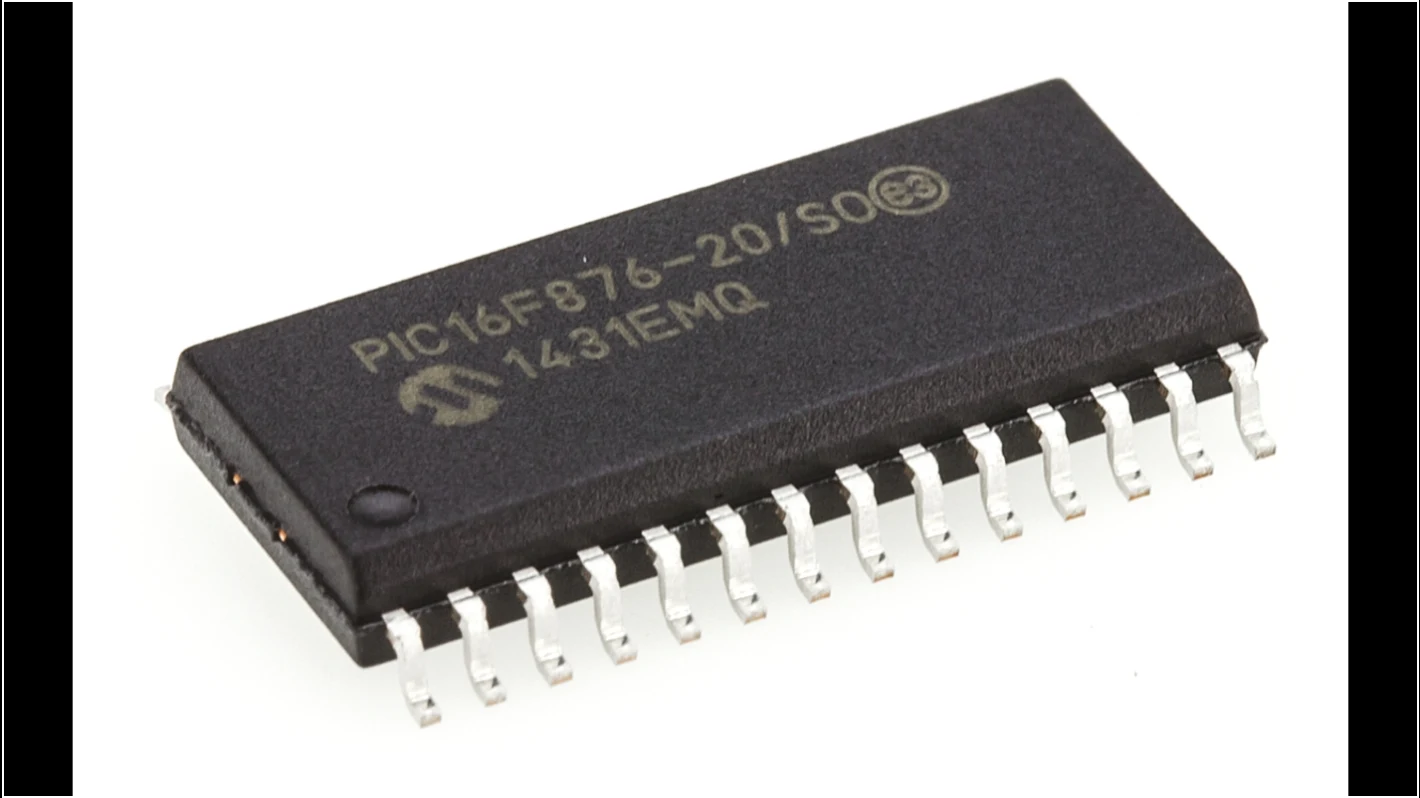
break MCU PIC16F876 lampu kilat melu retak perangkat kukuh ndhelik lan aman disimpen ing memori lampu kilat lan memori EEPROM. Unit mikrokontroler (MCU) PIC16F876 sing aman iki asring digunakake ing sistem sing dipasang, ing ngendi perangkat kukuh lan piranti lunak dilindhungi kanggo nyegah akses sing ora sah. Nalika nyoba ngrusak proteksi, teknik reverse engineering biasane digunakake kanggo decode utawa dekripsi data biner lan heksimal mikroprosesor PIC16F876 sing dikunci ing memori lampu kilat.
The process begins with analyzing the microprocessor’s architecture to identify and bypass the encryption protocols securing the firmware. Specialized tools are used to attack the encryption and unlock the flash memory, allowing access to the embedded program and source code. Once the protective measures are defeated, the firmware can be restored, cloned, or replicated for system diagnostics, repair, or further development.
Unlocking the PIC16F876 MCU’s flash memory allows for the recovery of critical software, which is particularly useful in situations where the original source code is lost, corrupted, or unavailable. Cloning the firmware ensures that the program can be duplicated for use in similar systems or to create backups for future use.
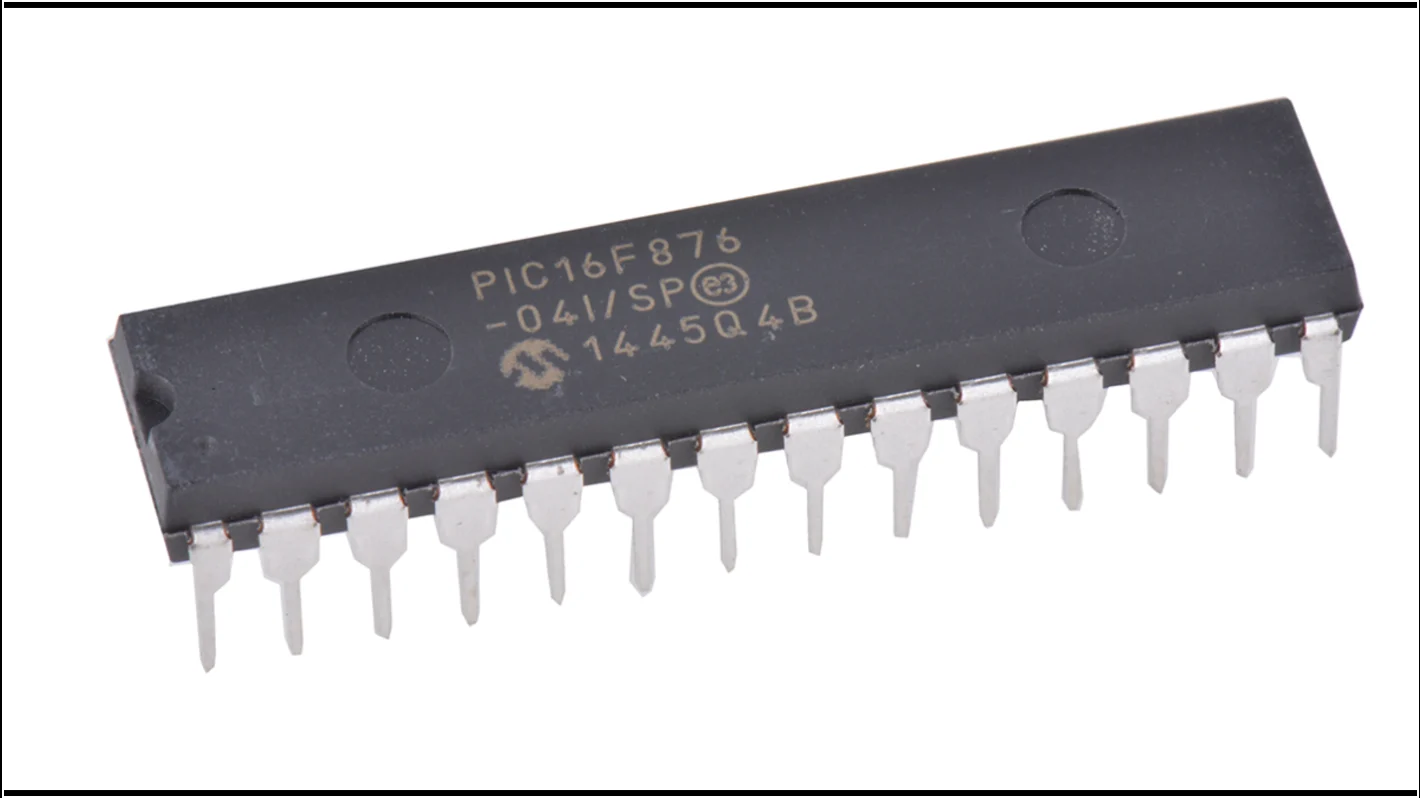
MCU PIC16F876 ఫ్లాష్ను విచ్ఛిన్నం చేయడంలో దాని ఫ్లాష్ మెమరీ మరియు EEPROM మెమరీలో నిల్వ చేయబడిన ఎన్క్రిప్టెడ్ మరియు సురక్షిత ఫర్మ్వేర్ను క్రాక్ చేయడం ఉంటుంది. ఈ సురక్షిత PIC16F876 మైక్రోకంట్రోలర్ యూనిట్ (MCU) తరచుగా ఎంబెడెడ్ సిస్టమ్లలో ఉపయోగించబడుతుంది, ఇక్కడ అనధికార ప్రాప్యతను నిరోధించడానికి దాని ఫర్మ్వేర్ మరియు సాఫ్ట్వేర్ రక్షించబడతాయి. రక్షణను విచ్ఛిన్నం చేయడానికి ప్రయత్నించినప్పుడు, ఫ్లాష్ మెమరీలో గుప్తీకరించిన PIC16F876 మైక్రోప్రాసెసర్ యొక్క లాక్ చేయబడిన బైనరీ మరియు హెక్సిమల్ డేటాను డీకోడ్ చేయడానికి లేదా డీక్రిప్ట్ చేయడానికి రివర్స్ ఇంజనీరింగ్ పద్ధతులు సాధారణంగా ఉపయోగించబడతాయి.
However, it is crucial to note that breaking the protection of an MCU like the PIC16F876 should be done within legal and ethical boundaries. Unauthorized decryption or cloning of the firmware could lead to intellectual property violations and legal consequences. As such, this process should be carried out responsibly, ensuring the preservation of both the software’s integrity and the rights of the original creators.
The STATUS register contains the arithmetic status of the ALU, the RESET status and the bank select bits for data memory. The STATUS register can be the destination for any instruction, as with any other register. If the STATUS register is the destination for an instruction that affects the Z, DC or C bits, then the write to these three bits is disabled.
These bits are set or cleared according to the device logic. Furthermore, the TO and PD bits are not writable, therefore, the result of an instruction with the STATUS register as destination may be different than intended for the purpose of Break IC SST89E58RD2A Software.
Break Mcu PIC16F876 Flash
For example, CLRF STATUS will clear the upper three bits and set the Z bit. This leaves the STATUS register as 000u u1uu (where u = unchanged). It is recommended, therefore, that only BCF, BSF, SWAPF and MOVWF instructions are used to alter the STATUS register, because these instructions do not affect the Z, C or DC bits from the STATUS register.
For other instructions not affecting any status bits, see the “Instruction Set Summary.”
The OPTION_REG Register is a breakable and writable register, which contains various control bits to configure the TMR0 prescaler/WDT postscaler (single assignable register known also as the prescaler), the External INT Interrupt, TMR0 and the weak pull-ups on PORTB.
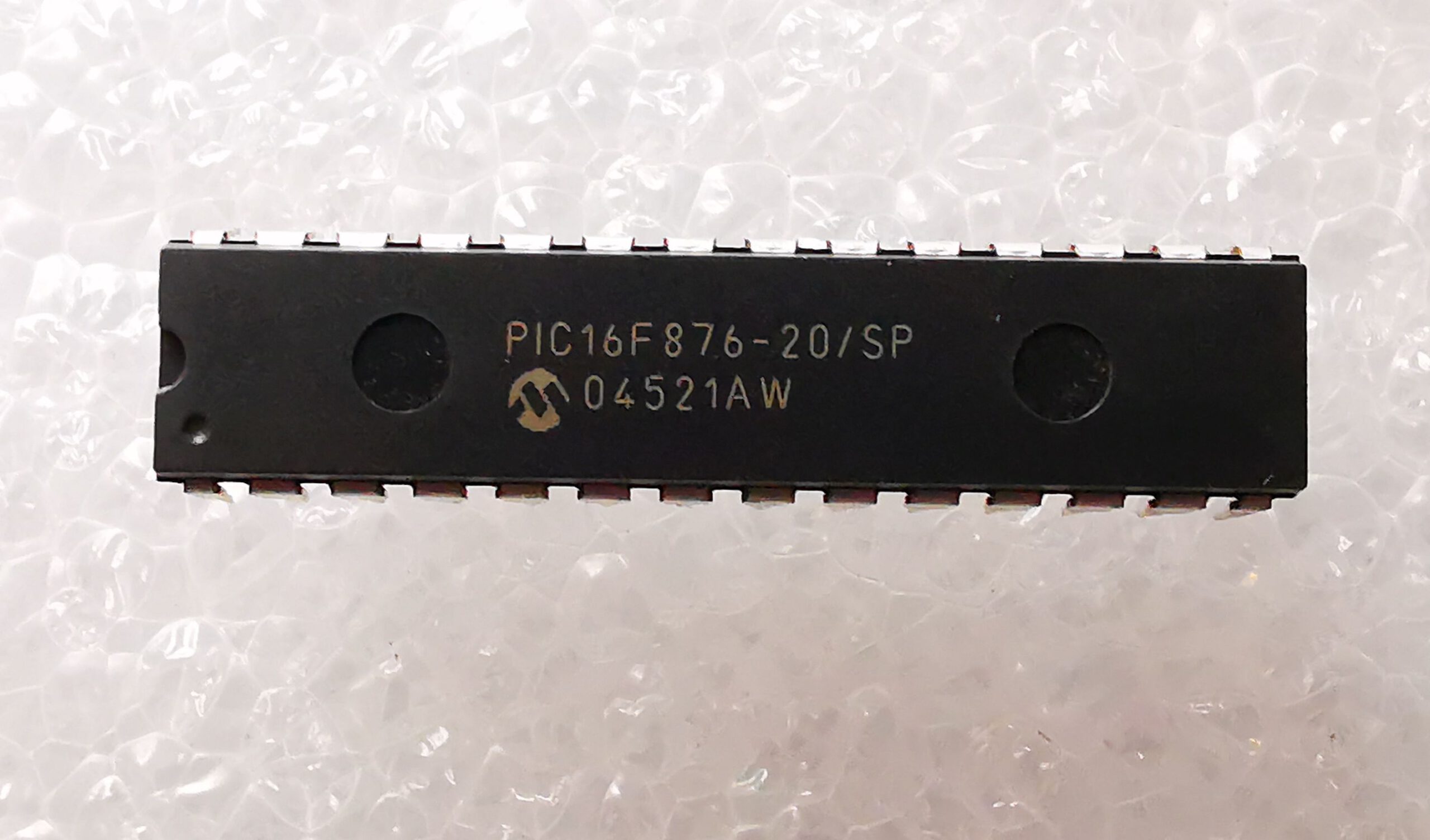
Um den Flash-Speicher des MCU PIC16F876 zu knacken, muss die verschlüsselte und gesicherte Firmware geknackt werden, die in seinem Flash-Speicher und EEPROM-Speicher gespeichert ist. Diese gesicherte Mikrocontrollereinheit (MCU) PIC16F876 wird häufig in eingebetteten Systemen verwendet, in denen die Firmware und Software vor unbefugtem Zugriff geschützt sind. Beim Versuch, den Schutz zu knacken, werden normalerweise Reverse-Engineering-Techniken eingesetzt, um die gesperrten binären und hexadezimalen Daten des verschlüsselten Mikroprozessors PIC16F876 im Flash-Speicher zu dekodieren oder zu entschlüsseln.
The program counter (PC) is 13-bits wide. The low byte comes from the PCL register, which is a breakable and writable register. The upper bits (PC<12:8>) are not breakable, but are indirectly writable through the PCLATH register to facilitate the process of Recover MCU DSPIC30F6013A30IP Firmware. On any RESET, the upper bits of the PC will be cleared. Figure 2-5 shows the two situations for the loading of the PC.
The upper example in the figure shows how the PC is loaded on a write to PCL (PCLATH<4:0> → PCH). The lower example in the figure shows how the PC is loaded during aCALL orGOTO instruction (PCLATH<4:3> → PCH). All PIC16F87X devices are capable of addressing a continuous 8K word block of program memory which is critical for Microcontroller Unlocking.
Break IC PIC16F876 Flash
The CALL and GOTO instructions provide only 11 bits of address to allow branching within any 2K program memory page. When doing aCALL or GOTO instruction, the upper 2 bits of the address are provided by PCLATH<4:3>. When doing a CALL or GOTO instruction, the user must ensure that the page select bits are programmed so that the desired program memory page is addressed before Break Mcu PIC16F876 Flash
If a return from a CALL instruction (or interrupt) is executed, the entire 13-bit PC is popped off the stack. Therefore, manipulation of the PCLATH<4:3> bits is not required for the return instructions (which POPs the address from the stack).
Break IC PIC16F873 Software
Breaking IC PIC16F873 software involves a series of techniques aimed at decrypting or cracking the encrypted firmware stored in its flash memory and EEPROM memory. The PIC16F873 microcontroller (MCU) is designed with secured protections that make its software, including binary and heximal data, difficult to access without proper authorization. However, reverse engineering and decryption techniques can be employed to unlock the locked firmware, enabling the extraction of the embedded program or source code for legitimate purposes.
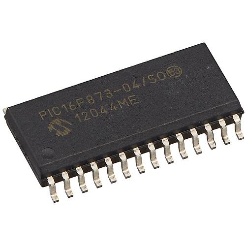
IC PIC16F873 yazılımını kırmak, flaş belleğinde ve EEPROM belleğinde saklanan şifreli aygıt yazılımını şifresini çözmeyi veya kırmayı amaçlayan bir dizi tekniği içerir. Güvenli PIC16F873 mikrodenetleyicisi (MCU), ikili ve onaltılık veriler de dahil olmak üzere yazılımına uygun yetkilendirme olmadan erişilmesini zorlaştıran güvenli korumalarla tasarlanmıştır. Ancak, kilitli mikroişlemci PIC16F873 tersine mühendislik ve şifre çözme teknikleri, kilitli aygıt yazılımını kilidini açmak için kullanılabilir ve gömülü programın veya kaynak kodunun meşru amaçlar için çıkarılmasını sağlar.
To begin the process, an attacker must first analyze the microprocessor’s architecture to understand how the protective mechanisms work. This may include studying the microcomputer’s memory layout, security features, and encryption algorithms. Once the firmware is identified, specialized tools and methods are used to break or crack the encryption, allowing the software to be decoded and recovered.
The goal of breaking the IC PIC16F873 software is often to restore functionality or replicate the program for backup purposes. In some cases, the source code is extracted to troubleshoot issues or enhance the program’s performance. Additionally, when cloning the software for use in other devices, the goal is to duplicate the program exactly as it exists in the original system.
However, it is crucial to note that breaking the software of an MCU like the PIC16F873 must be done within legal and ethical boundaries. Unauthorized access to locked firmware or decryption of encrypted data can violate intellectual property laws and lead to legal consequences.
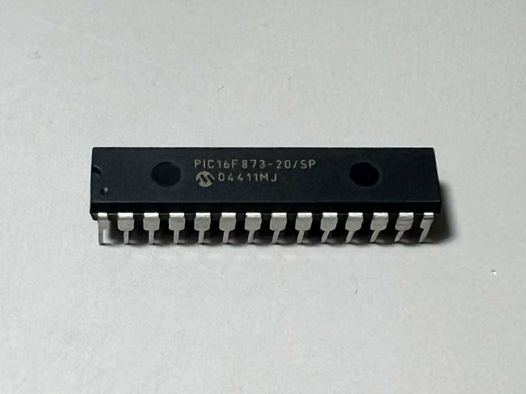
การทำลายซอฟต์แวร์ IC PIC16F873 เกี่ยวข้องกับเทคนิคชุดหนึ่งที่มุ่งเป้าไปที่การถอดรหัสหรือแคร็กเฟิร์มแวร์ที่เข้ารหัสซึ่งเก็บไว้ในหน่วยความจำแฟลชและหน่วยความจำ EEPROM ไมโครคอนโทรลเลอร์ (MCU) PIC16F873 ที่ปลอดภัยได้รับการออกแบบด้วยการป้องกันที่ปลอดภัยซึ่งทำให้ซอฟต์แวร์ซึ่งรวมถึงข้อมูลไบนารีและเลขฐานสิบหกเข้าถึงได้ยากหากไม่ได้รับอนุญาตอย่างเหมาะสม อย่างไรก็ตาม สามารถใช้เทคนิควิศวกรรมย้อนกลับและการถอดรหัสของไมโครโปรเซสเซอร์ PIC16F873 เพื่อปลดล็อกเฟิร์มแวร์ที่ถูกล็อค ทำให้สามารถแยกโปรแกรมที่ฝังไว้หรือโค้ดต้นฉบับเพื่อวัตถุประสงค์ที่ถูกต้องได้
In summary, breaking the IC PIC16F873 software involves cracking encryption, decoding binary data, and reverse engineering the firmware to access or restore critical software, while always adhering to ethical and legal standards.
We can Break IC PIC16F873 Software, please view the IC PIC16F873 features for your reference:
· High performance RISC CPU
· Only 35 single word instructions to learn
· All single cycle instructions except for program branches which are two cycle
· Operating speed: DC – 20 MHz clock input DC – 200 ns instruction cycle
· Up to 8K x 14 words of FLASH Program Memory, Up to 368 x 8 bytes of Data Memory (RAM) Up to 256 x 8 bytes of EEPROM Data Memory after the process of Break Microcontroller PIC16F767 Firmware
· Pinout compatible to the PIC16C73B/74B/76/77
· Interrupt capability (up to 14 sources)
· Eight level deep hardware stack
· Direct, indirect and relative addressing modes
· Power-on Reset (POR)
· Power-up Timer (PWRT) and Oscillator Start-up Timer (OST)
· Watchdog Timer (WDT) with its own on-chip RC oscillator for reliable operation
· Programmable code protection
· Power saving SLEEP mode
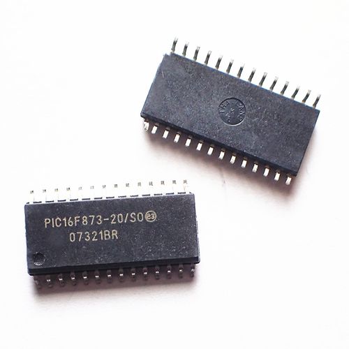
Phá vỡ phần mềm IC PIC16F873 liên quan đến một loạt các kỹ thuật nhằm giải mã hoặc bẻ khóa phần mềm được mã hóa được lưu trữ trong bộ nhớ flash và bộ nhớ EEPROM của nó. Bộ vi điều khiển (MCU) PIC16F873 được bảo mật được thiết kế với các biện pháp bảo vệ an toàn khiến phần mềm của nó, bao gồm dữ liệu nhị phân và thập lục phân, khó có thể truy cập nếu không có sự cho phép thích hợp. Tuy nhiên, kỹ thuật giải mã và kỹ thuật đảo ngược bộ vi xử lý PIC16F873 bị khóa có thể được sử dụng để mở khóa phần mềm bị khóa, cho phép trích xuất chương trình nhúng hoặc mã nguồn cho các mục đích hợp pháp.
· Selectable oscillator options
· Low power, high speed CMOS FLASH/EEPROM technology
· Fully static design
· In-Circuit Serial Programming (ICSP) via two pins
· Single 5V In-Circuit Serial Programming capability
· In-Circuit Debugging via two pins
· Processor break/write access to program memory by Break Chip PIC16F720 Firmware
· Wide operating voltage range: 2.0V to 5.5V
· High Sink/Source Current: 25 mA
· Commercial, Industrial and Extended temperature ranges
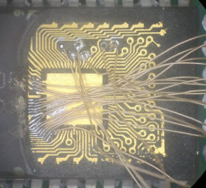
Break IC PIC16F873 Software
· Low-power consumption:
– < 0.6 mA typical @ 3V, 4 MHz
– 20 µA typical @ 3V, 32 kHz
– < 1 µA typical standby current
Peripheral Features:
· Timer0: 8-bit timer/counter with 8-bit prescaler
· Timer1: 16-bit timer/counter with prescaler, can be incremented during SLEEP via external crystal/clock
· Timer2: 8-bit timer/counter with 8-bit period register, prescaler and postscaler
· Two Capture, Compare, PWM modules
– Capture is 16-bit, max. resolution is 12.5 ns
– Compare is 16-bit, max. resolution is 200 ns
– PWM max. resolution is 10-bit
· 10-bit multi-channel Analog-to-Digital converter can provide a critical part for Microcontroller Unlock
· Synchronous Serial Port (SSP) with SPI (Master mode) and I2C (Master/Slave)
· Universal Synchronous Asynchronous Receiver Transmitter (USART/SCI) with 9-bit address detection
· Parallel Slave Port (PSP) 8-bits wide, with external RD, WR and CS controls (40/44-pin only)
· Brown-out detection circuitry for Brown-out Reset (BOR)