Archive for August, 2018
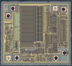
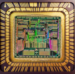
 Break Microchip PIC18F2553 Controller Protection
The power-managed mode that is invoked with the SLEEP instruction is determined by the setting of the IDLEN bit at the time the instruction is executed by Break Microchip PIC18F2553 Controller Protection. If another SLEEP instruction is executed, the device will enter the power-managed mode specified by IDLEN at that time. If IDLEN has changed, the device will enter the new power-managed mode specified by the new setting. Entry to, and exit from Idle mode, does not affect the state of the IDLEN bit.
In the Run modes, clocks to both the core and peripherals are active. The difference between these modes is the clock source. The PRI_RUN mode is the normal, full power execution mode of the microcontroller. This is also the default mode upon a device Reset, unless Two-Speed Start-up is enabled. In this mode, the OSTS bit is set. The IOFS bit may be set if the internal oscillator block is the primary clock source.
Break Microchip PIC18F2553 Controller Protection
The SEC_RUN mode is the compatible mode to the “clock switching” feature offered in other PIC18 devices. In this mode, the CPU and peripherals are clocked from the Timer1 oscillator. This gives users the option of lower power consumption while still using a high accuracy clock source.
SEC_RUN mode is entered by setting the SCS1:SCS0 bits to ‘01’. The device clock source is switched to the Timer1 oscillator (see Figure 3-1), the primary oscillator is shut down, the T1RUN bit (T1CON<6>) is set and the OSTS bit is cleared.
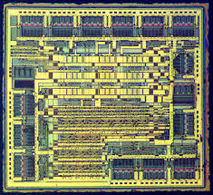
Recover PIC18F2539 Microcontroller Lost Heximal File
The length of the transition between clock sources is the sum of two cycles of the old clock source by Recover PIC18F2539 Microcontroller Lost Heximal File and three to four cycles of the new clock source. This formula assumes that the new clock source is stable.
Three bits indicate the current clock source and its status. They are:
- OSTS (OSCCON<3>)
- IOFS (OSCCON<2>)
- T1RUN (T1CON<6>)
In general, only one of these bits will be set while in a given power-managed mode. When the OSTS bit is set, the primary clock is providing the device clock by Break Nuvoton W78E054 MCU Flash. When the IOFS bit is set, the INTOSC output is providing a stable 8 MHz clock source to a divider that actually drives the device clock. When the T1RUN bit is set, the Timer1 oscillator is providing the clock. If none of these bits are set, then either the INTRC clock source is clocking the device, or the INTOSC source is not yet stable after Crack MCU Memory.
Recover PIC18F2539 Microcontroller Lost Heximal File
If the internal oscillator block is configured as the primary clock source by the FOSC3:FOSC0 Configuration bits in order to Attack Winbond W78E051A Protected Eeprom, then both the OSTS and IOFS bits may be set when in PRI_RUN or PRI_IDLE modes. This indicates that the primary clock (INTOSC output) is generating a stable 8 MHz output from Recover PIC18F2539 Microcontroller Lost Heximal File. Entering another power-managed RC mode at the same frequency would clear the OSTS bit.
Caution should be used when modifying a single IRCF bit through Reverse Engineering W78E52B Chip Data. If VDD is less than 3V, it is possible to select a higher clock speed than is supported by the low VDD. Improper device operation may result if the VDD/FOSC specifications are violated.
Executing a SLEEP instruction does not necessarily place the device into Sleep mode. It acts as the trigger to place the controller into either the Sleep mode or one of the Idle modes, depending on the setting of the IDLEN bit for the purpose of Winbond Microcontroller W78E0516 Embedded Binary Recovering.
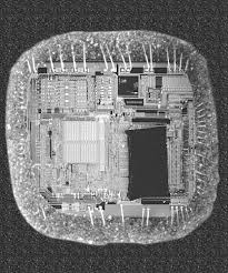
Break Microchip PIC18F2550 MCU Memory
PIC18F2550 devices offer a total of seven operating modes for more efficient power management by Crack MCU Firmware. These modes provide a variety of options for selective power conservation in applications where resources may be limited and Break Microchip PIC18F2550 MCU Memory (i.e., battery-powered devices).
There are three categories of power-managed modes:
• Run modes
• Idle modes
• Sleep mode
These categories define which portions of the device are clocked and sometimes, what speed. The Run and Idle modes may use any of the three available clock sources when Attack Microchip PIC18F2525 Processor Memory (primary, secondary or internal oscillator block). The Sleep mode does not use a clock source.
The power-managed modes include several power- saving features offered on previous PIC® devices. One is the clock switching feature, offered in other PIC18 devices, allowing the controller to use the Timer1 oscillator in place of the primary oscillator to facilitate the process of Reverse Engineering PIC18F2520 Controller. Also included is the Sleep mode, offered by all PIC devices, where all device clocks are stopped.
Break Microchip PIC18F2550 MCU Memory
Selecting a power-managed mode requires two decisions: if the CPU is to be clocked or not and the selection of a clock source. The IDLEN bit (OSCCON<7>) controls CPU clocking, while the SCS1:SCS0 bits (OSCCON<1:0>) select the clock source for the purpose of Break PIC18F2523 CPU Memory. The individual modes, bit settings, clock sources and affected modules are summarized in below Table.
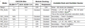
The SCS1:SCS0 bits allow the selection of one of three clock sources for power-managed modes. They are:
the primary clock, as defined by the FOSC3:FOSC0 Configuration bits to Microprocessor PIC18F2515 Heximal File Recovery
the secondary clock (the Timer1 oscillator)
the internal oscillator block (for RC modes)
Recover PIC18F2539 Microcontroller Embedded Eeprom
When PRI_IDLE mode is selected, the designated primary oscillator continues to run without interruption by Reverse Engineering Atmel MCU ATtiny48 Heximal. For all other power-managed modes, the oscillator using the OSC1 pin is disabled which will provide great benefit for Recover PIC18F2539 Microcontroller Embedded Eeprom. The OSC1 pin (and OSC2 pin, if used by the oscillator) will stop oscillating.
Recover PIC18F2539 Microcontroller Embedded Eeprom
In Secondary Clock modes (SEC_RUN and SEC_IDLE), the Timer1 oscillator is operating and providing the device clock. The Timer1 oscillator may also run in all power-managed modes if required to clock Timer1 or Timer3.
In Internal Oscillator modes (RC_RUN and RC_IDLE), the internal oscillator block provides the device clock source through Decrypt Encrypted Microcontroller ATmega16PA Code.
The 31 kHz INTRC output can be used directly to provide the clock and may be enabled to support various special features regardless of the power-managed mode after MCU Crack Process (see Section 23.2 “Watchdog Timer (WDT)”, Section 23.3 “Two-Speed Start-up” and Section 23.4 “Fail-Safe Clock Monitor” for more information on WDT, Fail-Safe Clock Monitor and Two- Speed Start-up).
The INTOSC output at 8 MHz may be used directly to clock the device or may be divided down by the postscaler. The INTOSC output is disabled if the clock is provided directly from the INTRC output to Recover PIC18F2539 Microcontroller Embedded Eeprom.
If the Sleep mode is selected, all clock sources are stopped. Since all the transistor switching currents have been stopped for the purpose of Reverse Engineering Locked Chip ATmega164PA Firmware, Sleep mode achieves the lowest current consumption of the device (only leakage currents).
Enabling any on-chip feature that will operate during Sleep will increase the current consumed during Sleep. The INTRC is required to support WDT operation. The Timer1 oscillator may be operating to support a Real-Time Clock. Other features may be operating that do not require a device clock source after Attack Atmel Chip ATmega2561V Secure Code (i.e., MSSP slave, PSP, INTn pins and others). Peripherals that may add significant current consumption are listed in Section 26.2 “DC Characteristics: Power-Down and Supply Current”.
Restore Microchip PIC18F2550 Memory Data
The OSTS, IOFS and T1RUN bits indicate which clock source is currently providing the device clock. The OSTS bit indicates that the Oscillator Start-up Timer by Restore Microchip PIC18F2550 Memory Data has timed out and the primary clock is providing the device clock in Primary Clock modes.
The IOFS bit indicates when the internal oscillator block has stabi- lized and is providing the device clock in RC Clock modes by Reverse Engineering Encrypted AVR Chip ATtiny261 Software. The T1RUN bit (T1CON<6>) indicates when the Timer1 oscillator is providing the device clock in Secondary Clock modes. In power-managed modes, only one of these three bits will be set at any time. If none of these bits are set, the INTRC is providing the clock or INTOSC has just started and is not yet stable.
The IDLEN bit determines if the device goes into Sleep mode or one of the Idle modes when the SLEEP instruction is executed through Decode Atmel Chip ATtiny461 Encrypted Firmware. The use of the flag and control bits in the OSCCON register is discussed in more detail in Section 3.0 “Power-Managed Modes”.
Restore Microchip PIC18F2550 Memory Data
Note 1: The Timer1 oscillator must be enabled to select the secondary clock source. The Timer1 oscillator is enabled by setting the T1OSCEN bit in the Timer1 Control register (T1CON<3>) in order to Break Encrypted Microprocessor ATtiny861 Embedded Heximal. If the Timer1 oscillator is not enabled, then any attempt to select a secondary clock source will be ignored.
2: It is recommended that the Timer1 oscillator be operating and stable before selecting the secondary clock source or a very long delay may occur while the Timer1 oscillator starts from Restore Microchip PIC18F2550 Memory Data.
PIC18LF2525 devices contain circuitry to prevent clock “glitches” when switching between clock sources. A short pause in the device clock occurs during the clock switch to Crack MCU Program. The length of this pause is the sum of two cycles of the old clock source and three to four cycles of the new clock source for the purpose of Break Atmel MCU ATmega1281 Locked Heximal. This formula assumes that the new clock source is stable. Clock transitions are discussed in greater detail in Section 3.1.2 “Entering Power-Managed Modes”.
Attack Microchip PIC18F2525 Processor Memory
The OSCCON register (Register 2-2) controls several aspects of the device clock’s operation which can provide critical support for Attack Microchip PIC18F2525 Processor Memory, both in full power operation and in power-managed modes to Decode Atmel AVR Processor ATMEGA169P Locked Code.
The System Clock Select bits, SCS1:SCS0, select the clock source. The available clock sources are the primary clock (defined by the FOSC3:FOSC0 Configu- ration bits), the secondary clock (Timer1 oscillator) and the internal oscillator block by Unlock Microcontroller Program. The clock source changes immediately after one or more of the bits is written to, following a brief clock transition interval. The SCS bits are cleared on all forms of Reset.
Attack Microchip PIC18F2525 Processor Memory
The Internal Oscillator Frequency Select bits (IRCF2:IRCF0) select the frequency output of the internal oscillator block to drive the device clock. The choices are the INTRC source, the INTOSC source (8 MHz) or one of the frequencies derived from the INTOSC postscaler for the purpose of Break Protected AVR Chip ATTINY24V Firmware (31.25 kHz to 4 MHz).
If the internal oscillator block is supplying the device clock, changing the states of these bits will have an immedi- ate change on the internal oscillator’s output. On device Resets, the default output frequency of the internal oscillator block is set at 1 MHz.
When a nominal output frequency of 31 kHz is selected (IRCF2:IRCF0 = 000), users may choose which inter- nal oscillator acts as the source for Attack Microchip PIC18F2525 Processor Memory. This is done with the INTSRC bit in the OSCTUNE register (OSCTUNE<7>). Setting this bit selects INTOSC as a 31.25 kHz clock source by enabling the divide-by-256 output of the INTOSC postscaler.
Clearing INTSRC selects INTRC (nominally 31 kHz) as the clock source, and disables the INTOSC clock source.
This option allows users to select the tunable and more precise INTOSC as a clock source, while maintaining power savings with a very low clock speed in order to Recover ATMEL AVR ATTINY44V Flash Code. Regardless of the setting of INTSRC, INTRC always remains the clock source for features such as the Watchdog Timer and the Fail-Safe Clock Monitor.
Break PIC18F2523 CPU Memory
A CCP module can use free-running Timer1 (or Timer3), clocked by the internal oscillator block and an external event with a known period to Break PIC18F2523 CPU Memory (i.e., AC power frequency). The time of the first event is captured in the CCPRxH:CCPRxL registers and is recorded for use later. When the second event causes a capture, the time of the first event is subtracted from the time of the second event before Reverse engineering microchip mcu TS87C58X2 locked eeprom. Since the period of the external event is known, the time difference between events can be calculated.
Break PIC18F2523 CPU Memory
If the measured time is much greater than the calculated time, the internal oscillator block is running too fast; to compensate, decrement the OSCTUNE register. If the measured time is much less than the calculated time, the internal oscillator block is running too slow after duplicate avr microprocessor ATMEGA8PA protected firmware; to compensate, increment the OSCTUNE register.
Both timers are cleared, but the timer clocked by the reference generates interrupts. When an interrupt occurs, the internally clocked timer is read and both timers are cleared. If the internally clocked timer value is greater than expected in order to extract atmel microprocessor ATMEGA16PA firmware, then the internal oscillator block is running too fast. To adjust for this, decrement the OSCTUNE register.
Like previous PIC18 devices, the PIC18LF2523 family includes a feature that allows the device clock source to be switched from the main oscillator to an alternate low-frequency clock source. PIC18LF2523 devices offer two alternate clock sources. When an alternate clock source is enabled, the various power-managed operating modes are available for the purpose of reverse engineering ATMEL AVR Chip ATMEGA32A program file.
Essentially, there are three clock sources for these devices:
- Primary oscillators
- Secondary oscillators
- Internal oscillator block
The primary oscillators include the External Crystal and Resonator modes, the External RC modes, the External Clock modes and the internal oscillator block before Crack MCU Software. The particular mode is defined by the FOSC3:FOSC0 Configuration bits.
Reverse Engineering PIC18F2520 Controller
The factory calibrates the internal oscillator block output (INTOSC) for 8 MHz after Crack MCU Firmware. However, this frequency may drift as VDD or temperature changes, which can affect the process of Reverse Engineering PIC18F2520 Controller operation in a variety of ways. It is possible to adjust the INTOSC frequency by modifying the value in the OSCTUNE register. This has no effect on the INTRC clock source frequency by Restore Atmel Controller ATmega88P Source Code.
Tuning the INTOSC source requires knowing when to make the adjustment, in which direction it should be made and in some cases, how large a change is needed. Three compensation techniques are discussed in Section 2.6.5.1 “Compensating with the EUSART”, Section 2.6.5.2 “Compensating with the Timers” and Section 2.6.5.3 “Compensating with the CCP Module in Capture Mode”, but other techniques may be used when Recover Protected Microcontroller ATmega169V Internal Memory.
bit 7 INTSRC: Internal Oscillator Low-Frequency Source Select bit
1 = 31.25 kHz device clock derived from 8 MHz INTOSC source (divide-by-256 enabled)
0 = 31 kHz device clock derived directly from INTRC internal oscillator bit 6 PLLEN: Frequency Multiplier PLL for INTOSC Enable bit(1)
1 = PLL enabled for INTOSC (4 MHz and 8 MHz only)
0 = PLL disabled
bit 5 Unimplemented: Read as ‘0’
bit 4-0 TUN4:TUN0: Frequency Tuning bits
01111 = Maximum frequency
• •
• •
00001
00000 = Center frequency. Oscillator module is running at the calibrated frequency.
11111
• •
• •
10000 = Minimum frequency
An adjustment may be required when the EUSART begins to generate framing errors or receives data with errors while in Asynchronous mode by Clone Microprocessor Flash Memory Protection Method. Framing errors indicate that the device clock frequency is too high; to adjust for this, decrement the value in OSCTUNE to reduce the clock frequency by Reverse Engineering PIC18F2520 Controller.
Reverse Engineering PIC18F2520 Controller
On the other hand, errors in data may suggest that the clock speed is too low; to compensate, increment OSCTUNE to increase the clock frequency. This technique compares device clock speed to some reference clock for the purpose of Replicate Locked IC TS80C52X2 Heximal. Two timers may be used; one timer is clocked by the peripheral clock, while the other is clocked by a fixed reference source, such as the Timer1 oscillator.
Microprocessor PIC18F2515 Heximal File Recovery
Using the internal oscillator as the clock source when Crack MCU Flash eliminates the need for up to two external oscillator pins which will provide great benefit for Microprocessor PIC18F2515 Heximal File Recovery and can then be used for digital I/O. Two distinct configurations are available:
- In INTIO1 mode, the OSC2 pin outputs FOSC/4, while OSC1 functions as RA7 for digital input and output.
- In INTIO2 mode, OSC1 functions as RA7 and OSC2 functions as RA6, both for digital input and output.
The internal oscillator block is calibrated at the factory to produce an INTOSC output frequency of 8.0 MHz through the process of Restore Microprocessor Program Most Important Two Steps. The INTRC oscillator operates independently of the INTOSC source. Any changes in INTOSC across voltage and temperature are not necessarily reflected by changes in INTRC and vice versa.
Microprocessor PIC18F2515 Heximal File Recovery
The internal oscillator’s output has been calibrated at the factory but can be adjusted in the user’s application. This is done by writing to the OSCTUNE register (Register 2-1).
When the OSCTUNE register is modified, the INTOSC frequency will begin shifting to the new frequency. The INTOSC clock will stabilize within 1 ms by Break Atmel AVR MCU ATmega8535L Heximal. Code execution continues during this shift. There is no indication that the shift has occurred.
The OSCTUNE register also implements the INTSRC and PLLEN bits, which control certain features of the internal oscillator block. The INTSRC bit allows users to select which internal oscillator provides the clock source when the 31 kHz frequency option is selected for the purpose of Microprocessor PIC18F2515 Heximal File Recovery. This is covered in greater detail in Section 2.7.1 “Oscillator Control Register”.
The PLLEN bit controls the operation of the frequency multiplier, PLL, in Internal Oscillator modes after Recover Atmel AVR Controller ATmega48V Firmware.
The 4x frequency multiplier can be used with the internal oscillator block to produce faster device clock speeds than are normally possible with an internal oscillator. When enabled, the PLL produces a clock speed of up to 32 MHz. Unlike HSPLL mode, the PLL is controlled through software. The control bit, PLLEN (OSCTUNE<6>), is used to enable or disable its operation by Break IC ATmega88V Internal Flash.
The PLL is available for use with the INTOSC when:
- The primary clock is the INTOSC clock source (selected in CONFIG1H<3:0>), and
- The 4 or 8 MHz INTOSC output is selected.
Writes to the PLLEN bit will be ignored until both these conditions are met.
Break PIC18F2510 Microcontroller Flash Memory
A Phase Locked Loop (PLL) circuit is provided as an option for users who wish to use a lower frequency oscillator circuit which can be used for Break PIC18F2510 Microcontroller Flash Memory, or to clock the device up to its highest rated frequency from a crystal oscillator. This may be useful for customers who are concerned with EMI due to high-frequency crystals of Protected Winbond Microprocessor W78E65 Reverse Engineering, or users who require higher clock speeds from an internal oscillator.
The HSPLL mode makes use of the HS mode oscillator for frequencies up to 10 MHz. A PLL then multiplies the oscillator output frequency by 4 to produce an internal clock frequency up to 40 MHz. The PLLEN bit is not available in this oscillator mode after Winbond MCU W78E365 Heximal Data Restoration. The PLL is only available to the crystal oscillator when the FOSC3:FOSC0 Configuration bits are programmed for HSPLL mode (= 0110).
Break PIC18F2510 Microcontroller Flash Memory
The PLL is also available to the internal oscillator block when the INTOSC is configured as the primary clock source. In this configuration, the PLL is enabled in soft- ware and generates a clock output of up to 32 MHz. The operation of INTOSC with the PLL is described in Section 2.6.4 “PLL in INTOSC Modes” after Nuvoton Microcomputer W78E51B Encrypted Heximal Recovery.
The PIC18F2510 devices include an internal oscillator block which generates two different clock signals; either can be used as the microcontroller’s clock source. This may eliminate the need for external oscillator circuits on the OSC1 and/or OSC2 pins.
The main output (INTOSC) is an 8 MHz clock source, which can be used to directly drive the device clock. It also drives a postscaler, which can provide a range of clock frequencies from 31 kHz to 4 MHz. The INTOSC output is enabled when a clock frequency from 125 kHz to 8 MHz is selected, and can provide 31 kHz if required by Attack Nutovon Microcontroller W77E52 Flash Memory.
The other clock source is the internal RC oscillator (INTRC) which provides a nominal 31 kHz output. INTRC is enabled if it is selected as the device clock source; it is also enabled automatically when any of the following are enabled:
• Power-up Timer
• Fail-Safe Clock Monitor
• Watchdog Timer
These features are discussed in greater detail in Section 23.0 “Special Features of the CPU” after the process of Crack MCU Eeprom. The clock source frequency (INTOSC direct, INTRC direct or INTOSC postscaler) is selected by configuring the IRCF bits of the OSCCON register on Break PIC18F2510 Microcontroller Flash Memory. Additionally, the 31 kHz clock can be provided by either the INTOSC, or INTRC clock sources, depending on the INTSRC bit (OSCTUNE<7>).