Archive for August, 2018
 Microchip PIC18F4321 Processor Flash Breaking
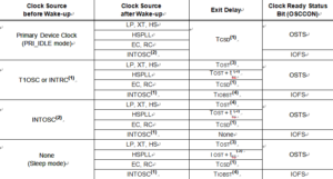
Normally, the device is held in Reset by the Oscillator Start-up Timer (OST) by Microchip PIC18F4321 Processor Flash Breaking until the primary clock becomes ready. At that time, the OSTS bit is set and the device begins executing code. If the internal oscillator block is the new clock source, the IOFS bit is set instead when Unlock Microcontroller Flash.
The exit delay time from Reset to the start of code execution depends on both the clock sources before and after the wake-up and the type of oscillator if the new clock source is the primary clock by Open IC PIC16F73 Memory,. Exit delays are summarized in below Table.
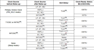
Code execution can begin before the primary clock becomes ready. If either the Two-Speed Start-up (see Section 23.3 “Two-Speed Start-up”) or Fail-Safe Clock Monitor (see Section 23.4 “Fail-Safe Clock Monitor”) is enabled, the device may begin execution as soon as the Reset source has cleared when Break Secured MCU PIC16F72 Data.
Microchip PIC18F4321 Processor Flash Breaking
Execution is clocked by the INTOSC multiplexer driven by the inter- nal oscillator block. Execution is clocked by the internal oscillator block until either the primary clock becomes ready or a power-managed mode is entered before the primary clock becomes ready; the primary clock is then shut down by Recover IC PIC16LF506 Data.
Certain exits from power-managed modes do not invoke the OST at all. There are two cases:
• PRI_IDLE mode, where the primary clock source is not stopped and
• the primary clock source is not any of the LP, XT, HS or HSPLL modes.
In these instances, the primary clock source is either already running (PRI_IDLE), or normally does not require an oscillator start-up delay (RC, EC and INTIO Oscillator modes). However, a fixed delay of interval TCSD following the wake event is still required when leaving Sleep and Idle modes to allow the CPU to prepare for execution when Decrypt Locked IC PIC16LF505 Program. Instruction execution resumes on the first clock cycle following this delay.
Recover PIC18F4221 MCU Embedded Program
This section discusses Resets generated by MCLR, POR and BOR and covers the operation of the various start-up timers from Recover PIC18F4221 MCU Embedded Program. Stack Reset events are covered in Section 5.1.2.4 “Stack Full and Underflow Resets”. WDT Resets are covered in Section 23.2 “Watchdog Timer (WDT)”.
The PIC18F4221 devices differentiate between various kinds of Reset:
a) Power-on Reset (POR)
b) MCLR Reset during normal operation
c) MCLR Reset during power-managed modes
d) Watchdog Timer (WDT) Reset (during execution)
e) Programmable Brown-out Reset (BOR)
f) RESET Instruction
g) Stack Full Reset
h) Stack Underflow Reset
A simplified block diagram of the on-chip Reset circuit is shown in below Figure.
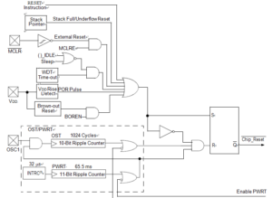
Device Reset events are tracked through the RCON register (Register 4-1). The lower five bits of the regis- ter indicate that a specific Reset event has occurred. In most cases, these bits can only be cleared by the event and must be set by the application after the event of Crack MCU Memory.
Recover PIC18F4221 MCU Embedded Program
The state of these flag bits, taken together, can be read to indicate the type of Reset that just occurred when Break MCU PIC16LF73 Heximal, This is described in more detail in Section 4.6 “Reset State of Registers”.
The RCON register also has control bits for setting interrupt priority (IPEN) and software control of the BOR (SBOREN) in order to Decrypt LOCKED MCU PIC16LF72 Heximal. Interrupt priority is discussed in Section 9.0 “Interrupts”. BOR is covered in Section 4.4 “Brown-out Reset (BOR)”.
Break PIC18F4220 Microcontroller Flash Memory
Normally, the device is held in Reset by the Oscillator Start-up Timer (OST) until the primary clock becomes ready from Break PIC18F4220 Microcontroller Flash Memory. At that time, the OSTS bit is set and the device begins executing code. If the internal oscillator block is the new clock source, the IOFS bit is set instead to Reverse Engineering ATMEL chip AT32UC3C264C flash.
The exit delay time from Reset to the start of code execution depends on both the clock sources before and after the wake-up and the type of oscillator if the new clock source is the primary clock from Reverse Engineering Chip ATMEGA644A code, Exit delays are summarized in below Table.
Code execution can begin before the primary clock becomes ready. If either the Two-Speed Start-up (see Section 23.3 “Two-Speed Start-up”) or Fail-Safe Clock Monitor (see Section 23.4 “Fail-Safe Clock Monitor”) is enabled, the device may begin execution as soon as the Reset source has cleared after Unlock Microcontroller Eeprom.
Execution is clocked by the INTOSC multiplexer driven by the inter- nal oscillator block. Execution is clocked by the internal oscillator block until either the primary clock becomes ready or a power-managed mode is entered before the primary clock becomes ready before Reverse Engineering Microcontroller ATmega644PA firmware; the primary clock is then shut down.
Break PIC18F4220 Microcontroller Flash Memory
Certain exits from power-managed modes do not invoke the OST at all. There are two cases:
• PRI_IDLE mode, where the primary clock source is not stopped and
• the primary clock source is not any of the LP, XT, HS or HSPLL modes.
In these instances, the primary clock source is either already running (PRI_IDLE), or normally does not require an oscillator start-up delay (RC, EC and INTIO Oscillator modes) by Recover MCU ATmega162A Heximal. However, a fixed delay of interval TCSD following the wake event is still required when leaving Sleep and Idle modes to Break PIC18F4220 Microcontroller Flash Memory. Instruction execution resumes on the first clock cycle following this delay.
Reverse PIC18F2685 MCU Eprom Code
An exit from Sleep mode or any of the Idle modes is triggered by an interrupt from Crack MCU Program, a Reset or a WDT time-out. This section discusses the triggers that cause exits from power-managed modes from Reverse PIC18F2685 MCU Eprom Code. The clocking subsystem actions are discussed in each of the power-managed modes.
Any of the available interrupt sources can cause the device to exit from an Idle mode or the Sleep mode to a Run mode. To enable this functionality, an interrupt source must be enabled by setting its enable bit in one of the INTCON or PIE registers when Reverse Engineering MCU ATMEGA324PV heximal, The exit sequence is initiated when the corresponding interrupt flag bit is set.
On all exits from Idle or Sleep modes by interrupt, code execution branches to the interrupt vector if the GIE/ GIEH bit (INTCON<7>) is set. Otherwise, code execution continues or resumes without branching.
Reverse PIC18F2685 MCU Eprom Code
A fixed delay of interval TCSD following the wake event is required when leaving Sleep and Idle modes. This delay is required for the CPU to prepare for execution after Recover MCU ATMEGA324A firmware. Instruction execution resumes on the first clock cycle following this delay.
A WDT time-out will cause different actions depending on which power-managed mode the device is in when the time-out occurs. If the device is not executing code (all Idle modes and Sleep mode), the time-out will result in an exit from the power-managed mode for the purpose of Break Microcontroller ATmega324PA binary, If the device is executing code from Reverse PIC18F2685 MCU Eprom Code (all Run modes), the time-out will result in a WDT Reset.
The WDT timer and postscaler are cleared by executing a SLEEP or CLRWDT instruction, the loss of a currently selected clock source (if the Fail-Safe Clock Monitor is enabled) and modifying the IRCF bits in the OSCCON register from Break IC ATMEGA644 eeprom if the internal oscillator block is the device clock source.
Recover PIC18F2682 Microcontroller Flash Program
In RC_IDLE mode, the CPU is disabled but the peripherals continue to be clocked from the internal oscillator block using the INTOSC multiplexer which is also critical for Recover PIC18F2682 Microcontroller Flash Program. This mode allows for controllable power conservation during Idle periods. From RC_RUN, this mode is entered by setting the IDLEN bit and executing a SLEEP instruction when Crack MCU Eeprom.
If the device is in another Run mode, first set IDLEN, then set the SCS1 bit and execute SLEEP of Break chip ATMEGA861P code. Although its value is ignored, it is recommended that SCS0 also be cleared; this is to maintain software compatibility with future devices. The INTOSC multiplexer may be used to select a higher clock frequency by modifying the IRCF bits before executing the SLEEP instruction.
When the clock source is switched to the INTOSC multiplexer, the primary oscillator is shut down and the OSTS bit is cleared. If the IRCF bits are set to any non-zero value, or the INTSRC bit is set, the INTOSC output is enabled. The IOFS bit becomes set of Recover Microprocessor ATmega640V firmware, after the INTOSC output becomes stable, after an interval of TIOBST.

Recover PIC18F2682 Microcontroller Flash Program
Clocks to the peripherals continue while the INTOSC source stabilizes. If the IRCF bits were previously at a non-zero value to Reverse Engineering MCU ATtiny48V eeprom or INTSRC was set before the SLEEP instruction was executed and the INTOSC source was already stable, the IOFS bit will remain set by Recover PIC18F2682 Microcontroller Flash Program. If the IRCF bits and INTSRC are all clear, the INTOSC output will not be enabled, the
IOFS bit will remain clear and there will be no indication of the current clock source. When a wake event occurs, the peripherals continue to be clocked from the INTOSC multiplexer. After a delay of TCSD following the wake event, the CPU begins executing code being clocked by the INTOSC multiplexer to support the process of Recover Microcontroller ATmega324V data, The IDLEN and SCS bits are not affected by the wakeup. The INTRC source will continue to run if either the WDT or the Fail-Safe Clock Monitor is enabled.
Break PIC18F2680 MCU Eeprom Memory
This mode is unique among the three low-power Idle modes, in that it does not disable the primary device clock when Break PIC18F2680 MCU Eeprom Memory. For timing sensitive applications, this allows for the fastest resumption of device operation with its more accurate primary clock source, since the clock source does not have to “warm-up” or transition from another oscillator when Recover Locked Chip ATMEGA128PV Binary.
Break PIC18F2680 MCU Eeprom Memory
PRI_IDLE mode is entered from PRI_RUN mode by setting the IDLEN bit and executing a SLEEP instruction when Crack MCU Firmware. If the device is in another Run mode, set IDLEN first, then clear the SCS bits and execute SLEEP to Decrypt Locked MCU ATMEGA128V Embedded Firmware. Although the CPU is disabled, the peripherals continue to be clocked from the primary clock source specified by the FOSC3:FOSC0 Configuration bits. The OSTS bit remains set (see below Figure).
![]()
When a wake event occurs, the CPU is clocked from the primary clock source. A delay of interval TCSD is required between the wake event and when code execution starts. This is required to allow the CPU to become ready to execute instructions. After the wake- up, the OSTS bit remains set. The IDLEN and SCS bits are not affected by the wake-up for the purpose of Dump Microcontroller ATMEGA128V Locked Code (see below Figure).
![]()
The Timer1 oscillator should already be running prior to entering SEC_IDLE mode. If the T1OSCEN bit is not set when the SLEEP instruction is executed, the SLEEP instruction will be ignored and entry to SEC_IDLE mode will not occur through Decrypt Microprocessor ATMEGA169PA Code. If the Timer1 oscillator is enabled but not yet running, peripheral clocks will be delayed until the oscillator has started. In such sit- uations, initial oscillator operation is far from stable and unpredictable operation may result.
Recover PIC18F2620 Microprocessor Eeprom Program
The Idle modes allow the controller’s CPU to be Recover PIC18F2620 Microprocessor Eeprom Program while the peripherals continue to operate. Selecting a particular Idle mode allows users to further manage power consumption.
If the IDLEN bit is set to a ‘1’ when a SLEEP instruction is executed, the peripherals will be clocked from the clock source selected using the SCS1:SCS0 bits; however, the CPU will not be clocked. The clock source status bits are not affected when Break IC ATmega640A Secured Flash. Setting IDLEN and executing a SLEEP instruction provides a quick method of switching from a given Run mode to its corresponding Idle mode.
If the WDT is selected, the INTRC source will continue to operate. If the Timer1 oscillator is enabled, it will also continue to run. Since the CPU is not executing instructions, the only exits from any of the Idle modes are by interrupt, WDT time-out or a Reset to prevent the process of Decrypt Secured MCU ATMEGA128P Code.
Recover PIC18F2620 Microprocessor Eeprom Program
When a wake event occurs, CPU execution is delayed by an interval of TCSD (parameter 38, Table 26-10) while it becomes ready to execute code when Crack MCU Flash. When the CPU begins executing code from Recover PIC18F2620 Microprocessor Eeprom Program, it resumes with the same clock source for the current Idle mode.
For example, when waking from RC_IDLE mode, the internal oscillator block will clock the CPU and peripherals (in other words, RC_RUN mode). The IDLEN and SCS bits are not affected by the wake-up for the purpose of Reverse Engineering IC ATMEGA88PV Locked Flash. While in any Idle mode or the Sleep mode, a WDT time-out will result in a WDT wake-up to the Run mode currently specified by the SCS1:SCS0 bits.
Break PIC18F2610 MCU Flash Memory
The power-managed Sleep mode in the PIC18F2610 devices is identical to the legacy Sleep mode offered in all other PIC devices. It is entered by clearing the IDLEN bit (the default state on device Reset) and executing the SLEEP instruction which faciliate the process of Break PIC18F2610 MCU Flash Memory.
This shuts down the selected oscillator (below Figure) after Break IC PIC12F615 Software. All clock source status bits are cleared. Entering the Sleep mode from any other mode does not require a clock switch to Break IC PIC12F635 Program. This is because no clocks are needed once the controller has entered Sleep. If the WDT is selected, the INTRC source will continue to operate. If the Timer1 oscillator is enabled for the purpose of Break IC PIC16F616 Heximal, it will also continue to run.
![]()
When a wake event occurs in Sleep mode (by interrupt, Reset or WDT time-out), the device will not be clocked until the clock source selected by the SCS1:SCS0 bits becomes ready (see Figure 3-6), or it will be clocked from the internal oscillator block when Break IC PIC12F609 Heximal if either the Two-Speed Start-up or the Fail-Safe Clock Monitor are enabled (see Section 23.0 “Special Features of the CPU”).
In either case, the OSTS bit is set when the primary clock is providing the device clocks. The IDLEN and SCS bits are not affected by the wake-up from Crack MCU Software.
Break PIC18F2610 MCU Flash Memory
Reverse Engineering PIC18F2580 Processor Embedded Software
This mode is entered by setting the SCS1 bit to ‘1’. Although it is ignored, it is recommended that the SCS0 bit also be cleared; this is to maintain software compatibility with future devices. When the clock source is switched to the INTOSC multiplexer when Break IC ATmega324V Protected Firmware (see below Figure), the primary oscillator is shut down and the OSTS bit is cleared by Reverse Engineering PIC18F2580 Processor Embedded Software. The IRCF bits may be modified at any time to immediately change the clock speed.
![]()
Caution should be used when modifying a single IRCF bit. If VDD is less than 3V, it is possible to select a higher clock speed than is supported by the low VDD. Improper device operation may result if the VDD/FOSC specifications are violated for the purpose of Decode Locked Microprocessor ATmega324A Source Code.
If the IRCF bits and the INTSRC bit are all clear, the INTOSC output is not enabled and the IOFS bit will remain clear; there will be no indication of the current clock source. The INTRC source is providing the device clocks.
If the IRCF bits are changed from all clear (thus, enabling the INTOSC output) or if INTSRC is set by Crack MCU Eeprom, the IOFS bit becomes set after the INTOSC output becomes stable. Clocks to the device continue while the INTOSC source stabilizes after an interval of TIOBST.
Reverse Engineering PIC18F2580 Processor Embedded Software
If the IRCF bits were previously at a non-zero value, or if INTSRC was set before setting SCS1 and the INTOSC source was already stable, the IOFS bit will remain set by Dump Microcontroller ATMEGA1284V Source Code.
On transitions from RC_RUN mode to PRI_RUN mode, the device continues to be clocked from the INTOSC multiplexer while the primary clock is started. When the primary clock becomes ready for Reverse Engineering PIC18F2580 Processor Embedded Software, a clock switch to the pri- mary clock occurs (see below Figure).
When the clock switch is complete, the IOFS bit is cleared, the OSTS bit is set and the primary clock is providing the device clock. The IDLEN and SCS bits are not affected by the switch from Reverse Engineering Chip ATmega640PV Locked Flash. The INTRC source will continue to run if either the WDT or the Fail-Safe Clock Monitor is enabled.
![]()
Microchip PIC18F2553 MCU Heximal Recovering
The Timer1 oscillator should already be running prior to entering SEC_RUN mode which is necessary for Microchip PIC18F2553 MCU Heximal Recovering. If the T1OSCEN bit is not set when the SCS1:SCS0 bits are set to ‘01’, entry to SEC_RUN mode will not occur for Microchip PIC18F2520 Embedded Firmware Extraction. If the Timer1 oscillator is enabled, but not yet running, device clocks will be delayed until the oscillator has started. In such situa- tions, initial oscillator operation is far from stable and unpredictable operation may result.
On transitions from SEC_RUN to PRI_RUN mode, the peripherals and CPU continue to be clocked from the Timer1 oscillator while the primary clock is started. When the primary clock becomes ready, a clock switch back to the primary clock occurs (see below Figure). When the clock switch is complete, the T1RUN bit is cleared, the OSTS bit is set and the primary clock is providing the clock to Microchip MCU PIC16F870 Heximal Code Restoration. The IDLEN and SCS bits are not affected by the wake-up; the Timer1 oscillator continues to run.
![]()
In RC_RUN mode, the CPU and peripherals are clocked from the internal oscillator block using the INTOSC multiplexer. In this mode, the primary clock is shut down in order to Recover Freescale MCU MC9S12XDG128 Memory Program. When using the INTRC source, this mode provides the best power conservation of all the Run modes, while still executing code in the process of Microchip PIC18F2553 MCU Heximal Recovering. It works well for user applications which are not highly timing sensitive or do not require high-speed clocks at all times.
Microchip PIC18F2553 MCU Heximal Recovering
If the primary clock source is the internal oscillator block (either INTRC or INTOSC), there are no distinguishable differences between PRI_RUN and RC_RUN modes during MCU Crack execution. However, a clock switch delay will occur during entry to and exit from RC_RUN mode which can be carried out by Reverse Engineering Microchip PIC16F1913 Memory. Therefore, if the primary clock source is the internal oscillator block, the use of RC_RUN mode is not recommended.