Archive for January, 2010
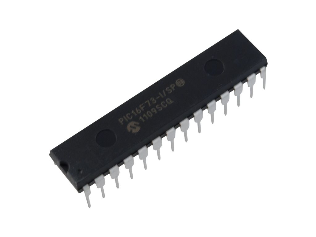
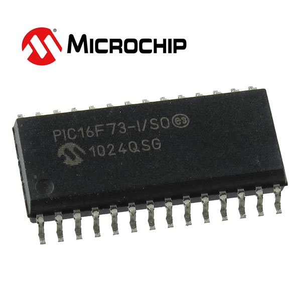
 Recover MCU PIC16F73 Binary
Recover MCU PIC16F73 Binary from flash memory and data extracted from eeprom memory of Microcontroller, reprogramme the firmware into blank MCU PIC16F73 for Microprocessor cloning;
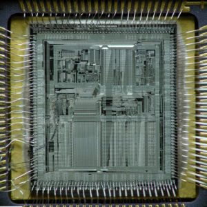
Recover MCU PIC16F73 Binary from flash memory and data extracted from eeprom memory of Microcontroller, reprogramme the firmware into blank MCU PIC16F73 for Microprocessor cloning
High Performance RISC CPU:
· High performance RISC CPU
· Only 35 single word instructions to learn
· All single cycle instructions except for program branches which are two-cycle
· Operating speed: DC – 20 MHz clock input DC – 200 ns instruction cycle
· Up to 8K x 14 words of FLASH Program Memory, Up to 368 x 8 bytes of Data Memory (RAM)
· Pinout compatible to the PIC16C73B/74B/76/77
· Pinout compatible to the PIC16F873/874/876/877
· Interrupt capability (up to 12 sources)
· Eight level deep hardware stack
· Direct, Indirect and Relative Addressing modes
· Processor read access to program memory
Special Microcontroller Features:
· Power-on Reset (POR)
· Power-up Timer (PWRT) and
Oscillator Start-up Timer (OST)
unlock PIC16F73 microprocessor fuse bit and open mcu flash memory and eeprom memory to readout heximal program and binary data
· Watchdog Timer (WDT) with its own on-chip RC oscillator for reliable operation
· Programmable code protection
· Power saving SLEEP mode
· Selectable oscillator options
· In-Circuit Serial Programming (ICSP) via two pins
Peripheral Features:
· Timer0: 8-bit timer/counter with 8-bit prescaler
· Timer1: 16-bit timer/counter with prescaler, can be incremented during SLEEP via external crystal/clock
· Timer2: 8-bit timer/counter with 8-bit period register, prescaler and postscaler
· Two Capture, Compare, PWM modules if Recover mcu binary
– Capture is 16-bit, max. resolution is 12.5 ns
– Compare is 16-bit, max. resolution is 200 ns
– PWM max. resolution is 10-bit
recover pic16F73 mcu chip flash memory code and clone the program firmware to new microcontroller
· 8-bit, up to 8-channel Analog-to-Digital converter
· Synchronous Serial Port (SSP) with SPI (Master mode) and I2C (Slave)
· Universal Synchronous Asynchronous Receiver Transmitter (USART/SCI)
· Parallel Slave Port (PSP), 8-bits wide with external RD, WR and CS controls (40/44-pin only)
· Brown-out detection circuitry for Brown-out Reset (BOR)
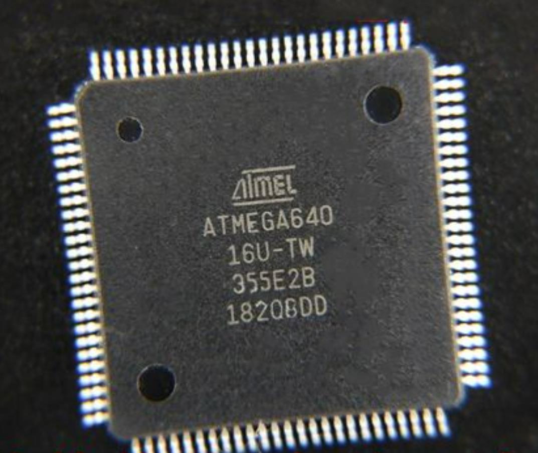
Recover Chip ATmega640P Heximal
Recover Chip ATmega640P Heximal from Microcontroller ATmega640P flash and eeprom memory, rewrite the firmware to blank MCU ATmega640P by Microprocessor copying technique, unlock MCU secured system and reset the status of Microcontroller from locked to unlocked;
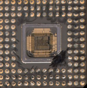
Recover Chip ATmega640P Heximal from Microcontroller ATmega640P flash and eeprom memory, rewrite the firmware to blank MCU ATmega640P by Microprocessor copying technique, unlock MCU secured system and reset the status of Microcontroller from locked to unlocked
In non-PWM waveform generation modes, the match output of the comparator can be forced by writing a one to the Force Output Compare (FOC0x) bit. Forcing Compare Match will not set the OCF0x Flag or reload/clear the timer, but the OC0x pin will be updated as if a real Compare Match had occurred (the COM0x1:0 bits settings define whether the OC0x pin is set, cleared or toggled) if MCU PIC16F917 heximal breaking.
All CPU write operations to the TCNT0 Register will block any Compare Match that occur in the next timer clock cycle, even when the timer is stopped. This feature allows OCR0x to be initialized to the same value as TCNT0 without triggering an interrupt when the Timer/Counter clock is enabled.
Since writing TCNT0 in any mode of operation will block all Compare Matches for one timer clock cycle, there are risks involved when changing TCNT0 when using the Output Compare Unit, independently of whether the Timer/Counter is running or not after recover MCU PIC16F72 code.
If the value written to TCNT0 equals the OCR0x value, the Compare Match will be missed, resulting in incorrect waveform generation. Similarly, do not write the TCNT0 value equal to BOTTOM when the counter is down-counting.
microprocessor atmega640v protection unlocking and readout embedded firmware
The setup of the OC0x should be performed before setting the Data Direction Register for the port pin to output. The easiest way of setting the OC0x value is to use the Force Output Compare (FOC0x) strobe bits in Normal mode if recover MCU PIC16F77 eeprom heximal.
The OC0x Registers keep their values even when changing between Waveform Generation modes. Be aware that the COM0x1:0 bits are not double buffered together with the compare value. Changing the COM0x1:0 bits will take effect immediately.
Recover MCU PIC16F72A Firmware
Recover MCU PIC16F72A Firmware in the format of binary or heximal, reset the configurate bits of Microcontroller PIC16F72A from locked to open one by crack microcontroller fuse bit, then readout code from MCU;
Recover MCU PIC16F72A Firmware in the format of binary or heximal, reset the configurate bits of Microcontroller PIC16F72A from locked to open one by crack microcontroller fuse bit, then readout code from MCU
This document contains device specific information for the operation of the PIC16F72 device. Additional information may be found in the PIC™ Mid-Range MCU Reference Manual (DS33023), which may be downloaded from the Microchip website. The Reference Manual should be considered a complementary document to this data sheet, and is highly recommended reading for a better understanding of the device architecture and operation of the peripheral modules.
The PIC16F72 belongs to the Mid-Range family of the PIC devices. The program memory contains 2K words, which translate to 2048 instructions, since each 14-bit program memory word is the same width as each device instruction. The data memory (RAM) contains 128 bytes after recover mcu AT89C4051 heximal.
There are 22 I/O pins that are user configurable on a pin-to-pin basis. Some pins are multiplexed with other device functions. These functions include:
· External interrupt
· Change on PORTB interrupt
· Timer0 clock input
· Timer1 clock/oscillator
· Capture/Compare/PWM
· A/D converter
· SPI/I2C
Table 1-1 details the pinout of the device with descriptions and details for each pin.
There are two memory blocks in the PIC16F72 device. These are the program memory and the data memory. Each block has separate buses so that concurrent access can occur. Program memory and data memory are explained in this section. Program memory can be read internally by the user code (see Section 7.0).
crack mcu PIC16F72A fuse bit and dump embedded firmware file from flash and eeprom memory
The data memory can further be broken down into the general purpose RAM and the Special Function Registers (SFRs). The operation of the SFRs that control the “core” are described here. The SFRs used to control the peripheral modules are described in the section discussing each individual peripheral module.
Additional information on device memory may be found in the PIC™ Mid-Range Reference Manual, (DS33023).
PIC16F72 devices have a 13-bit program counter capable of addressing a 8K x 14 program memory space.
The address range for this program memory is 0000h 07FFh. Accessing a location above the physically implemented address will cause a wraparound.
decrypt PIC16F72A microcontroller fuse bit and readout flash program code and eeprom data heximal
The RESET Vector is at 0000h and the Interrupt Vector is at 0004h.
The Data Memory is partitioned into multiple banks that contain the General Purpose Registers and the Special Function Registers. Bits RP1 (STATUS<6>) and RP0 (STATUS<5>) are the bank select bits.
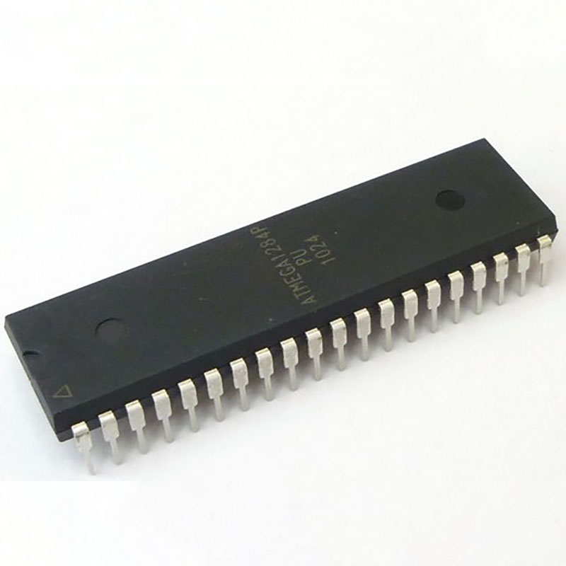
Reverse Engineering MCU ATmega1284V Heximal
Reverse Engineering MCU ATmega1284V by unlock microcontroller ATmega1284V protective system, and readout heximal from microprocessor program memory, rewrite to the firmware to new ATmega1284V;
Reverse Engineering MCU ATmega1284V by unlock microcontroller ATmega1284V protective system, and readout heximal from microprocessor program memory, rewrite to the firmware to new ATmega1284V
The 8-bit comparator continuously compares TCNT0 with the Output Compare Registers (OCR0A and OCR0B). Whenever TCNT0 equals OCR0A or OCR0B, the comparator signals a match. A match will set the Output Compare Flag (OCF0A or OCF0B) at the next timer clock cycle. If the corresponding interrupt is enabled, the Output Compare Flag generates an Output Compare interrupt if attacking PIC16F506 MCU code.
The Output Compare Flag is automatically cleared when the interrupt is executed. Alternatively, the flag can be cleared by software by writing a logical one to its I/O bit location. The Waveform Generator uses the match signal to generate an output according to operating mode set by the WGM02:0 bits and Compare Output mode (COM0x1:0) bits after copy microcontroller PIC16F747 code.
unlock ATMEGA1284P secured mcu fuse bit and extract embedded flash heximal file and eeprom binary program
The max and bottom signals are used by the Waveform Generator for handling the special cases of the extreme values in some modes of operation (“Modes of Operation” on page 121). Figure 40 shows a block diagram of the Output Compare unit. The OCR0x Registers are double buffered when using any of the Pulse Width Modulation (PWM) modes.
For the normal and Clear Timer on Compare (CTC) modes of operation, the double buffering is disabled. The double buffering synchronizes the update of the OCR0x Compare Registers to either top or bottom of the counting sequence.
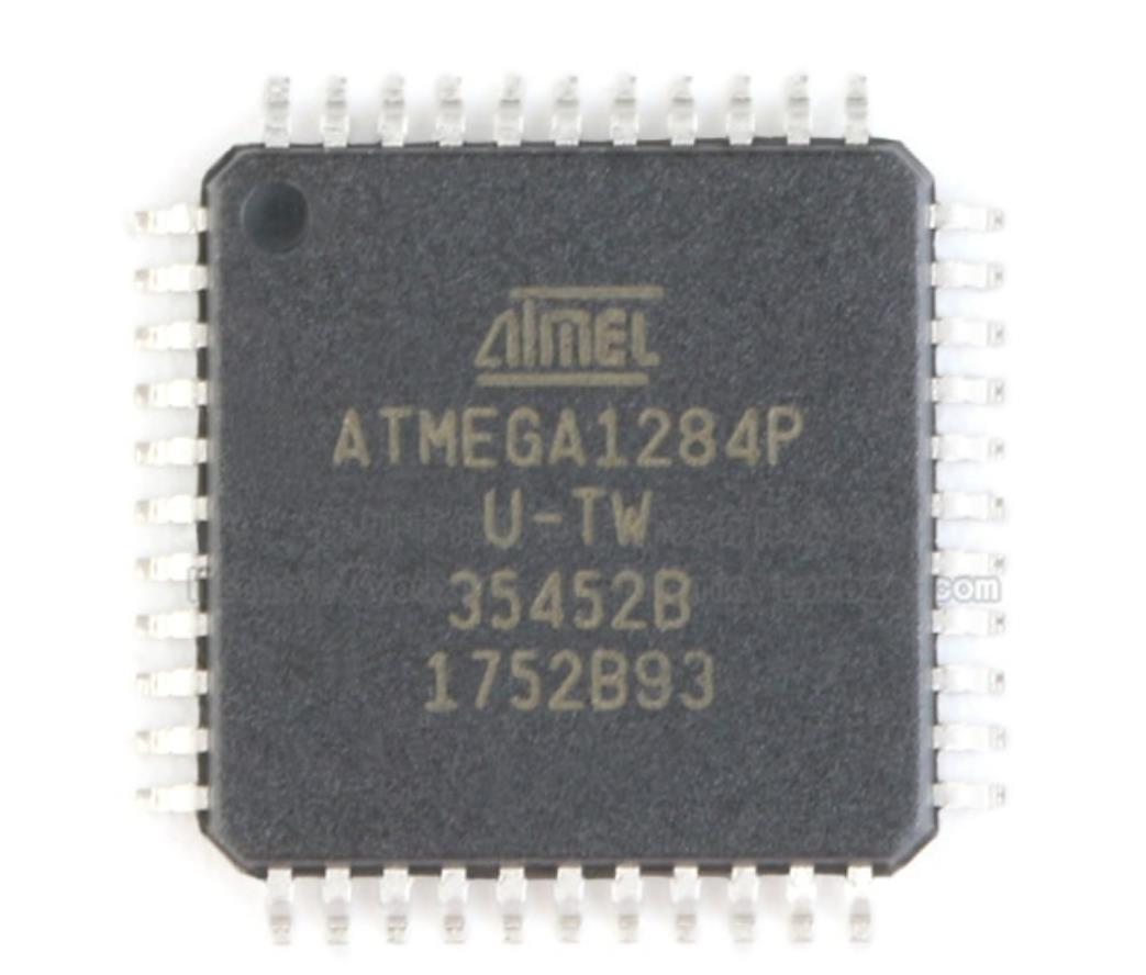
decrypt protected ATMEGA1284P controller and readout its flash firmware
The synchronization prevents the occurrence of odd-length, non-symmetrical PWM pulses, thereby making the output glitch-free. The OCR0x Register access may seem complex, but this is not case. When the double buffering is enabled, the CPU has access to the OCR0x Buffer Register, and if double buffering is disabled the CPU will access the OCR0x directly.
Break Chip ATmega1284V Code
Break Chip ATmega1284V security fuse bit by crack MCU ATmega1284V tamper resistance system, extract Microcontroller code from flash memory and eeprom memory;
Break Chip ATmega1284V security fuse bit by crack MCU ATmega1284V tamper resistance system, extract Microcontroller code from flash memory and eeprom memory
Many register and bit references in this section are written in general form. A lower case “n” replaces the Timer/Counter number, in this case 0. A lower case “x” replaces the Output Compare Unit, in this case Compare Unit A or Compare Unit B.
However, when using the register or bit defines in a program, the precise form must be used, i.e., TCNT0 for accessing Timer/Counter0 counter value and so on. The definitions in Table 69 are also used extensively throughout the document. The Timer/Counter can be clocked by an internal or an external clock source before chip PIC16F72A binary recovery.
The clock source is selected by the Clock Select logic which is controlled by the Clock Select (CS02:0) bits located in the Timer/Counter Control Register (TCCR0B), the main part of the 8-bit Timer/Counter is the programmable bi-directional counter unit. Figure 39 shows a block diagram of the counter and its surroundings when recover IC PIC16F687 software.
Depending of the mode of operation used, the counter is cleared, incremented, or decremented at each timer clock (clkT0). ClkT0 can be generated from an external or internal clock source, selected by the Clock Select bits (CS02:0). When no clock source is selected (CS02:0 = 0) the timer is stopped. However, the TCNT0 value can be accessed by the CPU, regardless of whether clkT0 is present or not. A CPU write overrides (has priority over) all counter clear or count operations.
The counting sequence is determined by the setting of the WGM01 and WGM00 bits located in the Timer/Counter Control Register (TCCR0A) and the WGM02 bit located in the Timer/Counter Control Register B (TCCR0B). There are close connections between how the counter behaves (counts) and how waveforms are generated on the Output Compare outputs OC0A and OC0B. The Timer/Counter Overflow Flag (TOV0) is set according to the mode of operation selected by the WGM02:0 bits. TOV0 can be used for generating a CPU interrupt.