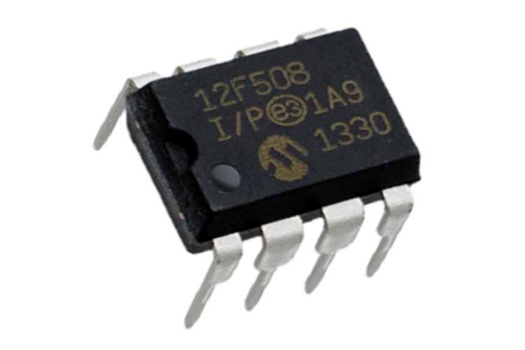
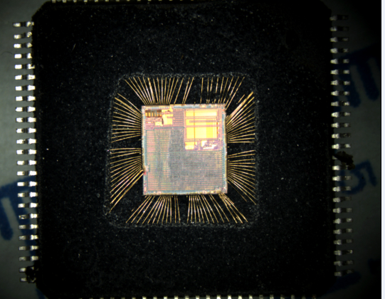
 Microchip PIC12F508 Processor Flash Memory Breaking
Microchip PIC12F508 Processor Flash Memory Breaking will disable the protection over the flash memory, original embedded firmware will be read through programmer;
Przerwanie pamięci flash procesora Microchip PIC12F508 spowoduje wyłączenie ochrony pamięci flash, oryginalne wbudowane oprogramowanie sprzętowe zostanie odczytane przez programator
If the low-power mode clock frequency is less than 1 MHz, the A/D RC clock source should be selected. Operation in the Low-Power Sleep mode requires the A/ D RC clock to be selected. If bits, ACQT2:ACQT0, are set to ‘000’ and a conversion is started, the conversion will be delayed one instruction cycle to allow execution of the SLEEP instruction and entry to Low-Power Sleep mode by recovering pic12f508 mcu source code. The IDLEN and SCS bits in the OSCCON register must have already been cleared prior to starting the conversion.
The ADCON1, TRISA and TRISB registers all configure the A/D port pins. The port pins needed as analog inputs must have their corresponding TRIS bits set (input). If the TRIS bit is cleared (output), the digital output level (VOH or VOL) will be converted. The A/D operation is independent of the state of the CHS2:CHS0 bits and the TRIS bits.
Mikrokontroler Microchip PIC12F508 łamie i wyodrębnia plik szesnastkowy z jego pamięci flash i pamięci eeprom,
When reading the Port register, all pins configured as analog input channels will read as cleared (a low level). Pins con- figured as digital inputs will convert an analog input. Analog levels on a digitally configured input will be accurately converted to decrypt locked chip pic12f508 firmware from its flash memory.
Analog levels on any pin defined as a digital input may cause the digital input buffer to consume current out of the device’s specification limits.
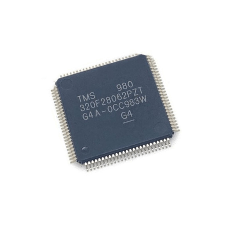
Reverse DSP MCU TMS320F28062PZT Flash Firmware
Reverse DSP MCU TMS320F28062PZT Flash Firmware is a process to unlock dsp microcontroller tms320f28062 encryption over its flash memory, and then the binary code will be readout from microprocessor tms320f28062pzt flash memory;
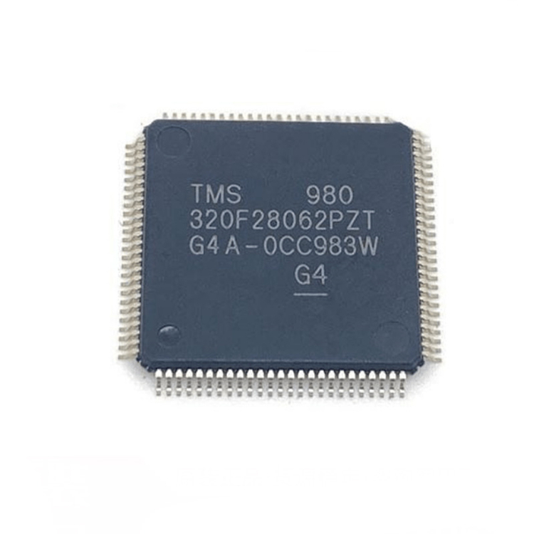
Reverse DSP MCU TMS320F28062PZT Flash Firmware is a process to unlock dsp microcontroller tms320f28062 encryption over its flash memory, and then the binary code will be readout from microprocessor tms320f28062pzt flash memory
The peripheral – I/O multiplexing implemented in the device prevents all available peripherals from being used at the same time. This is because more than one peripheral function may share an I/O pin. It is, however, possible to turn on the clocks to all the peripherals at the same time, although such a configuration is not useful. If this is done, the current drawn by the device will be more than the numbers specified in the current consumption tables.
The 2803x devices incorporate a method to reduce the device current consumption. Because each peripheral unit has an individual clock-enable bit, significant reduction in current consumption can be achieved by turning off the clock to any peripheral module that is not used in a given application. Furthermore, any one of the three low-power modes could be taken advantage of to reduce the current consumption even further. Table 7-1 indicates the typical reduction in current consumption achieved by turning off the clocks.
All peripheral clocks (except CPU Timer clock) are disabled upon reset. Writing to/reading from peripheral registers is possible only after the peripheral clocks are turned; This number represents the current drawn by the digital portion of the ADC module. Turning off the clock to the ADC module results in the elimination of the current drawn by the analog portion of the ADC (IDDA) as well.
Обратное прошивка DSP MCU TMS320F28062PZT Flash — это процесс разблокировки шифрования микроконтроллера tms320f28062 dsp через его флэш-память, после чего двоичный код будет считан из флэш-памяти микропроцессора tms320f28062pzt.
For peripherals with multiple instances, the current quoted is per For example, the 2 mA value quoted for ePWM is for one ePWM module.The baseline IDD current (current when the core is executing a dummy loop with no peripherals enabled) is 40 mA, typical. To arrive at the IDD current for a given application, the current-drawn by the peripherals (enabled by that application) must be added to the baseline IDD current.
Break Microchip PIC12F1571 MCU Protection
Break Microchip PIC12F1571 MCU Protection and read embedded firmware out from pic12f1571 microcontroller flash and eeprom memory, and then clone heximal program to new microprocessor PIC12F1571;
Break Microchip PIC12F1571 MCU Protection and read embedded firmware out from pic12f1571 microcontroller flash and eeprom memory, and then clone heximal program to new microprocessor PIC12F1571
PIC12F1257 microcontrollers combine the capabilities of 16-bit PWMs with Analog to suit a variety of applications. These devices deliver four 16-bit PWMs with independent timers for applications where high resolution is needed, such as LED lighting, stepper motors, power supplies and other general purpose applications which is useful.
The core independent peripherals (16-bit PWMs, Complementary Waveform Generator), Enhanced Universal Synchronous Asynchronous Receiver Transceiver (EUSART) and Analog (ADCs, Comparator and DAC) enable closed-loop feedback and communication for use in multiple market segments to restoring pic16f870 mcu heximal code.
The Peripheral Pin Select (PPS) functionality allows for I/O pin remapping of the digital peripherals for increased flexibility. The EUSART peripheral enables the communication for applications such as LIN.
Сломайте защиту микроконтроллера Microchip PIC12F1571 и прочитайте встроенную прошивку из флэш-памяти микроконтроллера pic12f1571 и памяти eeprom, а затем клонируйте шестнадцатеричную программу в новый микропроцессор PIC12F1571.
For the A/D converter to meet its specified accuracy, the charge holding capacitor (CHOLD) must be allowed to fully charge to the input channel voltage level. The analog input model is shown in Figure 17-2. The source impedance (RS) and the internal sampling switch (RSS) impedance directly affect the time required to charge the capacitor CHOLD by extracting mcu pic18f2520 embedded firmware.
The sampling switch (RSS) impedance varies over the device voltage (VDD). The source impedance affects the offset voltage at the analog input (due to pin leakage current). The maximum recommended impedance for analog sources is 2.5 kW. After the analog input channel is selected (changed), the channel must be sampled for at least the minimum acquisition time before starting a conversion.
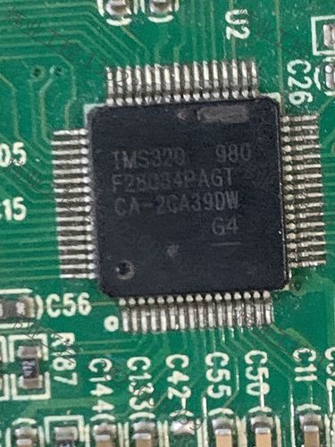
Restoring Texas Instrument TMS320F2806PZA MCU Flash OUT File
Restoring Texas Instrument TMS320F2806PZA MCU Flash OUT File needs to unlock the protection over dsp microcontroller tms320f2806pza flash memory, and extract the firmware code out from tms320f2806pza microprocessor memory;
The Enhanced USART module can receive a Break character in two ways.
The first method forces configuration of the baud rate at a frequency of 9/13 the typical speed. This allows for the Stop bit transition to be at the correct sampling location (12 bits for Break versus Start bit and eight data bits for typical data).
The second method uses the auto-wake-up feature described in Section 16.3.4 “Auto-Wake-up on Sync Break Character”. By enabling this feature, the EUSART will sample the next two transitions on RX/DT, cause an RCIF interrupt and receive the next data byte followed by another interrupt.
Note that following a Break character, the user will typically want to enable the Auto-Baud Rate Detect feature. For both methods, the user can set the ABD bit before placing the EUSART in its Sleep mode to crack locked mcu tms320f28069 flash memory protection.
Восстановление флэш-памяти микроконтроллера Texas Instrument TMS320F2806PZA OUT Файл необходим для разблокировки защиты флэш-памяти микроконтроллера tms320f2806pza dsp и извлечения кода прошивки из памяти микропроцессора tms320f2806pza.
The following sequence will send a message frame header made up of a Break, followed by an auto-baud Sync byte. This sequence is typical of a LIN bus master.
- Configure the EUSART for the desired mode.
- Set the TXEN and SENDB bits to set up the Break character.
- Load the TXREG with a dummy character to initiate transmission (the value is ignored).
- Write ‘55h’ to TXREG to load the Sync character into the transmit FIFO buffer.
After the Break has been sent, the SENDB bit is reset by hardware. The Sync character now transmits in the preconfigured mode to break dsp controller tms320f2806pza memory. When the TXREG becomes empty, as indicated by the TXIF, the next data byte can be written to TXREG.
Texas Instrument DSP TMS320F28069FPNT MCU Binary Restoration
Texas Instrument DSP TMS320F28069FPNT MCU Binary Restoration can be executed through cracking dsp locked microcontroller tms320f28069 fuse bit, then readout flash memory program from processor tms320f28069;
Based on the end application design and operational profile, the IDD and IDDIO currents could vary. Systems that exceed the recommended maximum power dissipation in the end product may require additional thermal enhancements. Ambient temperature (TA) varies with the end application and product design. The critical factor that affects reliability and functionality is TJ, the junction temperature, not the ambient temperature.
Hence, care should be taken to keep TJ within the specified limits. Tcase should be measured to estimate the operating junction temperature TJ. Tcase is normally measured at the center of the package top-side surface when breaking ti mcu tms320f28034png. The thermal application report Semiconductor and IC Package Thermal Metrics helps to understand the thermal metrics and definitions.
Восстановление двоичного кода микроконтроллера Texas Instrument DSP TMS320F28069FPNT может быть выполнено путем взлома заблокированного микроконтроллера tms320f28069 фьюз-бита dsp, а затем считывания программы флэш-памяти из процессора tms320f28069.
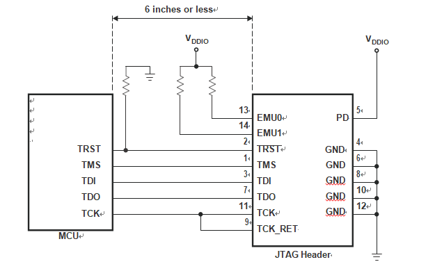
Below Figure shows the connection between the MCU and JTAG header for a single-processor configuration. If the distance between the JTAG header and the MCU is greater than 6 inches, the emulation signals must be buffered. If the distance is less than 6 inches to attack tms320f28235pg microprocessor protection system, buffering is typically not needed. Below Figure shows the simpler, no-buffering situation. For the pullup/pulldown resistor values, see Section 6.2, Signal Descriptions.
Recover Microprocessor TMS320F2801PZA Secured Flash Binary
Recover Microprocessor TMS320F2801PZA Secured Flash Binary and clone flash memory file to new dsp microcontroller tms320f2801pza, the original memory program will be readout from tms320f2801pza processor;
The baseline IDD current (current when the core is executing a dummy loop with no peripherals enabled) is 40 mA, typical. To arrive at the IDD current for a given application, the current-drawn by the peripherals (enabled by that application) must be added to the baseline IDD current.
Following are other methods to reduce power consumption further:
The flash module may be powered down if code is run off SARAM. This results in a current reduction of 18 mA (typical) in the VDD rail and 13 mA (typical) in the VDDIO rail to attack tms320f28027 mcu archive file from its flash memory.
Savings in IDDIO may be realized by disabling the pullups on pins that assume an output function.
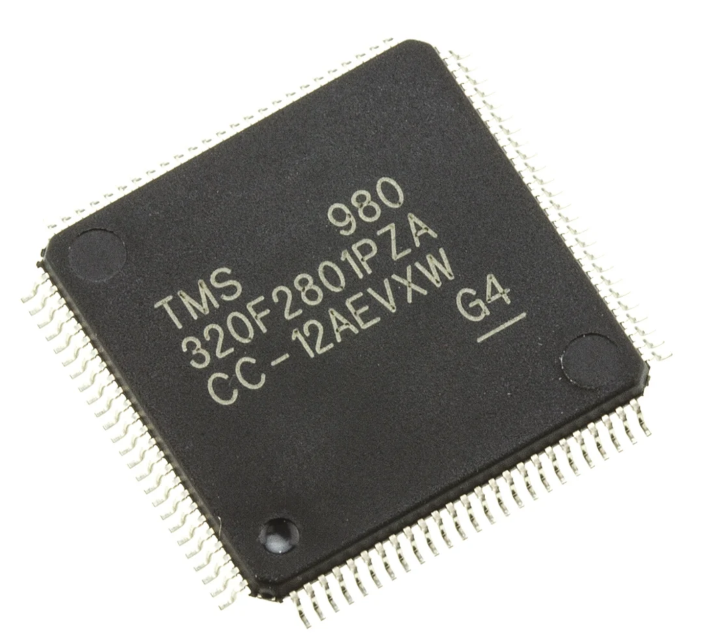
recuperar microprocesador TMS320F2801PZA asegurado binario flash y clonar archivo de memoria flash a nuevo microcontrolador dsp tms320f2801pza, el programa de memoria original será readout de procesador tms320f2801pza
To realize the lowest VDDA current consumption in a low-power mode, see the respective analog chapter of the TMS320F2803x Real-Time Microcontrollers Technical Reference Manual to ensure each module is powered down as well.
These values are based on a JEDEC defined 2S2P system (with the exception of the Theta JC [RΘJC] value, which is based on a JEDEC defined 1S0P system) and will change based on environment as well as application to . For more information, see these EIA/JEDEC standards:
JESD51-2, Integrated Circuits Thermal Test Method Environmental Conditions – Natural Convection (Still Air) by break ic tms320f28044 heximal from mcu;
JESD51-3, Low Effective Thermal Conductivity Test Board for Leaded Surface Mount Packages
JESD51-7, High Effective Thermal Conductivity Test Board for Leaded Surface Mount Packages
JESD51-9, Test Boards for Area Array Surface Mount Package Thermal Measurements
(2) lfm = linear feet per minute
Break DSP TMS320F2810PBKS Microcontroller Locked Memory
Break DSP TMS320F2810PBKS Microcontroller Locked Memory and extract mcu tms320f2810pb flash memory content, original embedded firmware will be restored from microprocessor tms320f2810pb dsp mcu;
The 2803x devices incorporate a method to reduce the device current consumption. Because each peripheral unit has an individual clock-enable bit, significant reduction in current consumption can be achieved by turning off the clock to any peripheral module that is not used in a given application.
romper DSP TMS320F2810PBKS microcontrolador bloqueado la memoria y extraer mcu tms320f2810pb contenido de la memoria flash, el firmware original incrustado será restaurado desde el microprocesador tms320f2810pb dsp mcu
Furthermore, any one of the three low-power modes could be taken advantage of to reduce the current consumption even further to attack ic mcu tms320f28232pg software. Below Table indicates the typical reduction in current consumption achieved by turning off the clocks.
All peripheral clocks (except CPU Timer clock) are disabled upon reset. Writing to/reading from peripheral registers is possible only after the peripheral clocks are turned on.
This number represents the current drawn by the digital portion of the ADC module to recover microcontroller tms320f2812pg firmware. Turning off the clock to the ADC module results in the elimination of the current drawn by the analog portion of the ADC (IDDA) as well.
For peripherals with multiple instances, the current quoted is per module. For example, the 2 mA value quoted for ePWM is for one ePWM module.
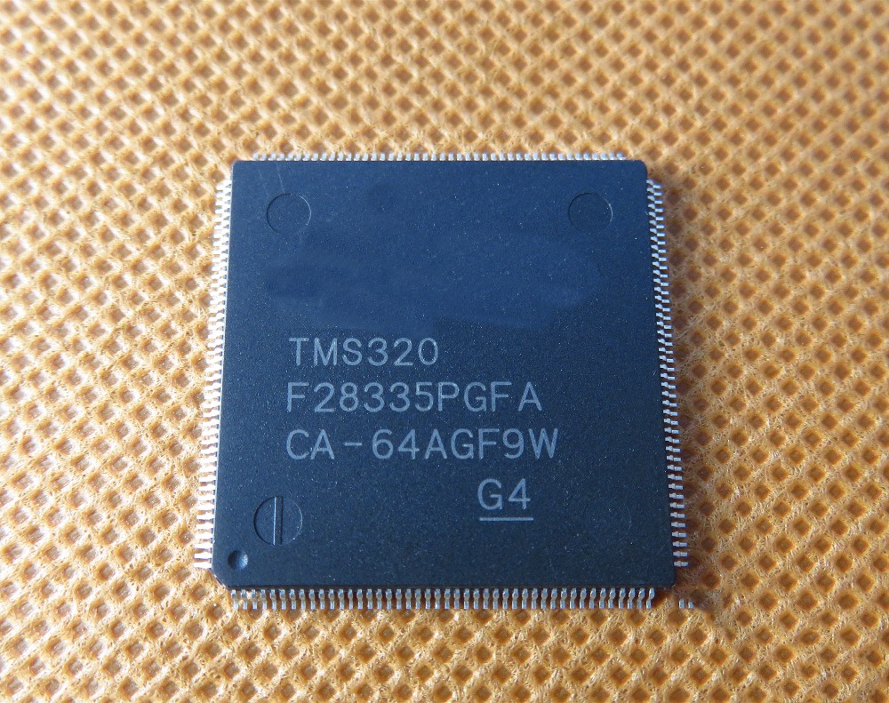
Attack TMS320F28235PG Microprocessor Protection System
Attack TMS320F28235PG Microprocessor Protection System and restore embedded binary file from mcu tms320f28235pg mcu flash memory;
If glitching is unacceptable in an application, 1.8 V could be supplied externally. Alternatively, adding a current-limiting resistor (for example, 470 Ω) in series with these pins and any external driver could be considered to limit the potential for degradation to the pin and/or external circuitry.
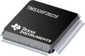
atacar el sistema de protección del microprocesador TMS320F28235PG y restaurar el archivo binario embebido de la memoria flash mcu tms320f28235pg mcu;
There is no power-sequencing requirement when using an external 1.8-V supply. However, if the 3.3-V transistors in the level-shifting output buffers of the I/O pins are powered before the 1.8-V transistors when extract texas instrument mcu tms320f2812pg code, it is possible for the output buffers to turn on, causing a glitch to occur on the pin during power up.
To avoid this behavior, power the VDD pins before or with the VDDIO pins, ensuring that the VDD pins have reached 0.7 V before the VDDIO pins reach 0.7 V.
The peripheral – I/O multiplexing implemented in the device prevents all available peripherals from being used at the same time. This is because more than one peripheral function may share an I/O pin to crack ti microcontroller tms320f28032 flash memory. It is, however, possible to turn on the clocks to all the peripherals at the same time, although such a configuration is not useful. If this is done, the current drawn by the device will be more than the numbers specified in the current consumption tables.
Texas Instruments TMS320F28034PNQ MCU Breaking
Texas Instruments TMS320F28034PNQ MCU Breaking is a process to unlock tms320f28034pnq controller’s flash memory and then readout embedded data from microcontroller tms320f28034pnq;

Section 6.2.1 describes the signals. With the exception of the JTAG pins, the GPIO function is the default at reset, unless otherwise mentioned. The peripheral signals that are listed under them are alternate functions. Some peripheral functions may not be available in all devices.
See Table 5-1 for details. Inputs are not 5-V tolerant. All GPIO pins are I/O/Z and have an internal pullup when reverse engineering dsp mcu tms320f28034 flash memory, which can be selectively enabled/disabled on a per-pin basis. This feature only applies to the GPIO pins.
Texas Instruments TMS320F28034PNQ MCU romper es un proceso para desbloquear tms320f28034pnq memoria flash del controlador y luego leer los datos incrustados de tms320f28034pnq microcontrolador;
The pullups on the PWM pins are not enabled at reset. The pullups on other GPIO pins are enabled upon reset. The AIO pins do not have an internal pullup.
When the on-chip VREG is used, the GPIO19, GPIO34, GPIO35, GPIO36, GPIO37, and GPIO38 pins could glitch during power up in order to recover secured dsp tms320f28035 microcontroller flash controller. This potential glitch will finish before the boot mode pins are read and will not affect boot behavior.
Microcontroller STM32F091VC Flash Heximal Recovery
Microcontroller STM32F091VC Flash Heximal Recovery needs to crack arm stm32f091vc microprocessor security fuse bit, duplicate flash firmware from arm mcu stm32f091vc;
Unless otherwise specified, the minimum and maximum values are guaranteed in the worst conditions of ambient temperature, supply voltage and frequencies by tests in production on 100% of the devices with an ambient temperature at TA = 25 °C and TA = TAmax (given by the selected temperature range).
Data based on characterization results, design simulation and/or technology characteristics are indicated in the table footnotes and are not tested in production to break stm32f301k6 encrypted microprocessor flash memory. Based on characterization, the minimum and maximum values refer to sample tests and represent the mean value plus or minus three times the standard deviation (mean±3s).
microcontrolador STM32F091VC flash heximal recuperación necesita para descifrar brazo stm32f091vc microprocesador seguridad fusible bit, duplicar flash firmware de brazo mcu stm32f091vc;
Unless otherwise specified, typical data are based on TA = 25 °C, VDD = VDDA = 3.3 V. They are given only as design guidelines and are not tested. Typical ADC accuracy values are determined by characterization of a batch of samples from a standard diffusion lot over the full temperature range when restoring secured stm32f301r8 mcu flash firmware, where 95% of the devices have an error less than or equal to the value indicated (mean±2s).