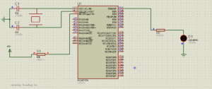
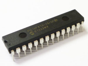
 Break IC PIC16F877A Heximal
The data EEPROM and Flash program memory is readable after Break IC PIC16F877A Heximal and writable during normal operation (over the full VDD range). This memory is not directly mapped in the register file space. Instead, it is indirectly addressed through the Special Function Registers. There are six SFRs used to read and write this memory:
EECON1
EECON2
EEDATA
EEDATH
EEADR
EEADRH
When interfacing to the data memory block, EEDATA holds the 8-bit data for read/write and EEADR holds the address of the EEPROM location being accessed. These devices have 128 or 256 bytes of data EEPROM (depending on the device), with an address range from 00h to FFh. On devices with 128 bytes, addresses from 80h to FFh are unimplemented and will wraparound to the beginning of data EEPROM memory to facilitate the process of Break IC PIC12F635 Program. When writing to unimplemented locations, the on-chip charge pump will be turned off.
When interfacing the program memory block, the EEDATA and EEDATH registers form a two-byte word that holds the 14-bit data for read/write and the EEADR and EEADRH registers form a two-byte word that holds the 13-bit address of the program memory location being accessed.
Break IC PIC16F877A Heximal
These devices have 4 or 8K words of program Flash, with an address range from 0000h to 0FFFh for the PIC16F873A/874A and 0000h to 1FFFh for the PIC16F876A/877A. Addresses above the range of the respective device will wraparound to the beginning of program memory.
The EEPROM data memory allows single-byte read and write. The Flash program memory allows single-word reads and four-word block writes.
Program memory write operations automatically perform an erase-before-write on blocks of four words. A byte write in data EEPROM memory automatically erases the location and writes the new data (erase-before-write) in order to Attack MCU PIC16F630 Firmware.
The write time is controlled by an on-chip timer. The write/erase voltages are generated by an on-chip charge pump, rated to operate over the voltage range of the device for byte or word operations. When the device is code-protected, the CPU may continue to read and write the data EEPROM memory.
Depending on the settings of the write-protect bits, the device may or may not be able to write certain blocks of the program memory; however, reads of the program memory are allowed. When code-protected, the device programmer can no longer access data or program for the purpose of Microcontroller Unlocking.
Break IC PIC16F876A Binary
There are three memory blocks in each of the PIC16F87XA devices, the hacker who is preparing Break IC PIC16F876A Binary needs to understand this. The program memory and data memory have separate buses so that concurrent access can occur and is detailed in this section. The EEPROM data memory block is detailed in Section 3.0.
“Data EEPROM and Flash Program Memory”. Additional information on device memory may be found in the PICmicro® Mid-Range MCU Family Reference Manual (DS33023)
PROGRAM MEMORY ORGANIZATION
The PIC16F87XA devices have a 13-bit program counter capable of addressing an 8K word x 14 bit program memory space. The PIC16F876A/877A devices have 8K words x 14 bits of Flash program memory, while PIC16F873A/874A devices have 4K words x 14 bits. Accessing a location above the physically implemented address will cause a wraparound
Break IC PIC16F876A Binary
The Reset vector is at 0000h and the interrupt vector is at 0004h.
DATA MEMORY ORGANIZATION
The data memory is partitioned into multiple banks which contain the General Purpose Registers and the Special Function Registers. Bits RP1 (Status<6>) and RP0 (Status<5>) are the bank select bits.
Each bank extends up to 7Fh (128 bytes). The lower locations of each bank are reserved for the Special Function Registers. Above the Special Function Registers are General Purpose Registers, implemented as static RAM. All implemented banks contain Special Function Registers. Some frequently used Special Function Registers from one bank may be mirrored in another bank for code reduction and quicker access for the purpose of Copy Microcontroller PIC16F639 Heximal.
The Special Function Registers are registers used by the CPU and peripheral modules for controlling the desired operation of the device. These registers are implemented as static RAM.
The Special Function Registers can be classified into two sets: core (CPU) and peripheral. Those registers associated with the core functions are described in detail in this section to faciliate the process of Break Chip PIC16F785 Heximal. Those related to the operation of the peripheral features are described in detail in the peripheral features section.
Break IC PIC16F874A Software
Acquained with CMOS Technology can greatly help to Break IC PIC16F874A Software:
· Low-power, high-speed Flash/EEPROM technology
· Fully static design
· Wide operating voltage range (2.0V to 5.5V)
· Commercial and Industrial temperature ranges
· Low-power consumption
PIC16F874A devices are available only in 28-pin packages, while PIC16F874A/877A devices are available in 40-pin and 44-pin packages. All devices in the PIC16F87XA family share common architecture with the following differences:
· The PIC16F873A and PIC16F874A have one-half of the total on-chip memory of the PIC16F876A and PIC16F877A
· The 28-pin devices have three I/O ports, while the 40/44-pin devices have five
· The 28-pin devices have fourteen interrupts, while the 40/44-pin devices have fifteen for the purpose
· The 28-pin devices have five A/D input channels, while the 40/44-pin devices have eight
· The Parallel Slave Port is implemented only on the 40/44-pin devices
Break IC PIC16F874A Software
The available features are summarized in Table 1-1. Block diagrams of the PIC16F873A/876A and PIC16F874A/877A devices are provided in Figure 1-1 and Figure 1-2, respectively.
The pinouts for these device families are listed in Table 1-2 and Table 1-3. Additional information may be found in the PICmicro Mid-Range Reference Manual (DS33023), which may be obtained from your local Microchip Sales Representative or downloaded from the Microchip web site.
The Reference Manual should be considered a complementary document to this data sheet and is highly recommended reading for a better understanding of the device architecture and operation of the peripheral modules.
Break IC PIC16F873A Code
Below we will introduce some basic features of PIC16F873A which will be useful for Break IC PIC16F873A Code
High-Performance RISC CPU:
· Only 35 single-word instructions to learn
· All single-cycle instructions except for program branches, which are two-cycle
· Operating speed: DC – 20 MHz clock input DC – 200 ns instruction cycle
· Up to 8K x 14 words of Flash Program Memory,
Up to 368 x 8 bytes of Data Memory (RAM),
Up to 256 x 8 bytes of EEPROM Data Memory
· Pinout compatible to other 28-pin or 40/44-pin PIC16CXXX and PIC16FXXX microcontrollers
Peripheral Features:
· Timer0: 8-bit timer/counter with 8-bit prescaler
· Timer1: 16-bit timer/counter with prescaler, can be incremented during Sleep via external crystal/clock
· Timer2: 8-bit timer/counter with 8-bit period register, prescaler and postscaler
Break IC PIC16F873A Code
· Two Capture, Compare, PWM modules
– Capture is 16-bit, max. resolution is 12.5 ns
– Compare is 16-bit, max. resolution is 200 ns
– PWM max. resolution is 10-bit
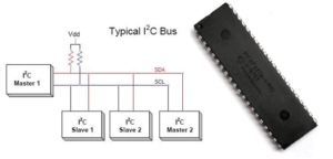
· Synchronous Serial Port (SSP) with SPI™ for the purpose
(Master mode) and I2C™ (Master/Slave)
· Universal Synchronous Asynchronous Receiver Transmitter (USART/SCI) with 9-bit address detection which can be used for Break MCU PIC18F442 Software
· Parallel Slave Port (PSP) – 8 bits wide with external RD, WR and CS controls (40/44-pin only)
· Brown-out detection circuitry for Brown-out Reset (BOR)
· Analog Comparator module with:
– Two analog comparators
– Programmable on-chip voltage reference (VREF) module
– Programmable input multiplexing from device inputs and internal voltage reference
– Comparator outputs are externally accessible
Special Microcontroller Features:
· 100,000 erase/write cycle Enhanced Flash program memory typical
· 1,000,000 erase/write cycle Data EEPROM memory typical
· Data EEPROM Retention > 40 years which is a very important point for Recover MCU PIC16F874 Code
· Self-reprogrammable under software control
· In-Circuit Serial Programming™ (ICSP™) via two pins
· Single-supply 5V In-Circuit Serial Programming
· Watchdog Timer (WDT) with its own on-chip RC oscillator for reliable operation
· Programmable code protection
· Power saving Sleep mode
· Selectable oscillator options
· In-Circuit Debug (ICD) via two pins Serial Port (SSP) with SPI™
(Master mode) and I2C™ (Master/Slave)
· Universal Synchronous Asynchronous Receiver Transmitter (USART/SCI) with 9-bit address detection
· Parallel Slave Port (PSP) – 8 bits wide with external RD, WR and CS controls (40/44-pin only)
· Brown-out detection circuitry for Brown-out Reset (BOR) which can ease the process of MCU Cracking.
Recover MCU PIC16F877 Program
Below we will discuss the basic structure of MCU PIC16F877 which will be useful for Recover MCU PIC16F877 Program:
High-Performance RISC CPU:
· Only 35 single-word instructions to learn
· All single-cycle instructions except for program branches, which are two-cycle
· Operating speed: DC – 20 MHz clock input DC – 200 ns instruction cycle
· Up to 8K x 14 words of Flash Program Memory,
Up to 368 x 8 bytes of Data Memory (RAM)
Up to 256 x 8 bytes of EEPROM Data Memory
Recover MCU PIC16F877 Program
· Pinout compatible to other 28-pin or 40/44-pin PIC16CXXX and PIC16FXXX microcontrollers
Peripheral Features:
· Timer0: 8-bit timer/counter with 8-bit prescaler
· Timer1: 16-bit timer/counter with prescaler, can be incremented during Sleep via external crystal/clock
· Timer2: 8-bit timer/counter with 8-bit period register, prescaler and postscaler
· Two Capture, Compare, PWM modules in the process of Break IC PIC16F873A Code
– Capture is 16-bit, max. resolution is 12.5 ns
– Compare is 16-bit, max. resolution is 200 ns
– PWM max. resolution is 10-bit if recover mcu
· Synchronous Serial Port (SSP) with SPI™ (Master mode) and I2C™ (Master/Slave)
· Universal Synchronous Asynchronous Receiver
Transmitter (USART/SCI) with 9-bit address detection
· Parallel Slave Port (PSP) – 8 bits wide with external RD, WR and CS controls (40/44-pin only)
· Brown-out detection circuitry for Brown-out Reset (BOR) to prevent the unauthorized Break IC PIC16F876A Binary
Analog Comparator module with:
– Two analog comparators
– Programmable on-chip voltage reference (VREF) module
– Programmable input multiplexing from device inputs and internal voltage reference
– Comparator outputs are externally accessible
Special Microcontroller Features:
· 100,000 erase/write cycle Enhanced Flash program memory typical
· 1,000,000 erase/write cycle Data EEPROM memory typical
· Data EEPROM Retention > 40 years
· Self-reprogrammable under software control
· In-Circuit Serial Programming™ (ICSP™) via two pins
· Single-supply 5V In-Circuit Serial Programming
· Watchdog Timer (WDT) with its own on-chip RC oscillator for reliable operation
· Programmable code protection which is good mechanism against MCU Cracking
· Power saving Sleep mode
· Selectable oscillator options
· In-Circuit Debug (ICD) via two pins
Recover MCU PIC16F877 Heximal
The STATUS register contains the arithmetic status of the ALU, the RESET status and the bank select bits for data memory. The STATUS register can be the destination for any instruction, as with any other register which will be very helpful to Recover MCU PIC16F877 Heximal. If the STATUS register is the destination for an instruction that affects the Z, DC or C bits, then the write to these three bits is disabled. These bits are set or cleared according to the device logic.
Furthermore, the TO and PD bits are not writable, therefore, the result of an instruction with the STATUS register as destination may be different than intended.
Recover MCU PIC16F877 Heximal
The OPTION_REG Register is a readable and writable register, which contains various control bits to configure the TMR0 prescaler/WDT postscaler (single assignable register known also as the prescaler), the External INT Interrupt, TMR0 and the weak pull-ups on PORTB STAT register is the destination for an instruction that affects the Z, DC or C bits, then the write to these three bits is disabled through the process of Recover MCU 12F508 Code.
These bits are set or cleared according to the situation
RBPU: PORTB Pull-up Enable bit
1 = PORTB pull-ups are disabled
0 = PORTB pull-ups are enabled by individual port latch values
INTEDG: Interrupt Edge Select bit
1 = Interrupt on rising edge of RB0/INT pin
0 = Interrupt on falling edge of RB0/INT pin
T0CS: TMR0 Clock Source Select bit
1 = Transition on RA4/T0CKI pin
0 = Internal instruction cycle clock (CLKOUT)
T0SE: TMR0 Source Edge Select bit
1 = Increment on high-to-low transition on RA4/T0CKI pin
0 = Increment on low-to-high transition on RA4/T0CKI pin
PSA: Prescaler Assignment bit
1 = Prescaler is assigned to the WDT
0 = Prescaler is assigned to the Timer0 module
PS2:PS0: Prescaler Rate Select bits
The INTCON Register is a readable and writable register, which contains various enable and flag bits for the TMR0 register overflow, RB Port change and External RB0/INT pin interrupts.
The PIC16F87X family has an 8-level deep x 13-bit wide hardware stack. The stack space is not part of either program or data space and the stack pointer is not readable or writable. The PC is PUSHed onto the stack when a CALL instruction is executed, or an interrupt causes a branch.
The stack is POPed in the event of a RETURN,RETLW or a RETFIE instruction execution. PCLATH is not affected by a PUSH or POP operation to tamper the attempt of Microcontroller Unlocking. The stack operates as a circular buffer. This means that after the stack has been PUSHed eight times after Recover MCU PIC16F877 Heximal.
All PIC16F87X devices are capable of addressing a continuous 8K word block of program memory. The CALL and GOTO instructions provide only 11 bits of address to allow branching within any 2K program memory page. When doing aCALL or GOTO instruction after Recover Chip PIC16F83 Eeprom, the upper 2 bits of the address are provided by PCLATH<4:3>.
When doing a CALL or GOTO instruction, the user must ensure that the page select bits are programmed so that the desired program memory page is addressed. If a return from a CALL instruction (or interrupt) is executed, the entire 13-bit PC is popped off the stack.
Recover MCU PIC16F876 Binary
MEMORY ORGANIZATION of PIC6F876 can help us better understand its structure and furthermore help to Recover MCU PIC16F876 Binary:
There are three memory blocks in each of the PIC16F87X MCUs. The Program Memory and Data Memory have separate buses so that concurrent access can occur when Crack MCU. The EEPROM data memory block is detailed in Section 4.0. Additional information on device memory may be found in the PICmicro Mid-Range Reference Manual, (DS33023).
Program Memory Organization
The PIC16F87X devices have a 13-bit program counter capable of addressing an 8K x 14 program memory space. The PIC16F877/876 devices have 8K x 14 words of FLASH program memory, and the PIC16F873/874 devices have 4K x 14. Accessing a location above the physically implemented address will cause a wraparound. The RESET vector is at 0000h and the interrupt vector is at 0004h only after Recover Chip PIC12CE518 Binary.
DATA MEMORY ORGANIZATION
Recover MCU PIC16F876 Binary
The data memory is partitioned into multiple banks which contain the General Purpose Registers and the Special Function Registers. Bits RP1 (STATUS<6>) and RP0 (STATUS<5>) are the bank select bits.
Each bank extends up to 7Fh (128 bytes). The lower Locations of each bank are reserved for the Special Function Registers. Above the Special Function Registers are General Purpose Registers, implemented as static RAM. All implemented banks contain Special Function Registers. Some frequently used Special Function Registers from one bank may be mirrored in another bank for code reduction and quicker access.
SPECIAL FUNCTION REGISTER
The Special Function Registers are registers used by the CPU and peripheral modules for controlling the desired operation of the device. These registers are implemented as static RAM for the purpose of Recovery MCU PIC16C662 Heximal.
The Special Function Registers can be classified into two sets: core (CPU) and peripheral. Those registers associated with the core functions are described in detail in this section. Those related to the operation of the peripheral features are described in detail in the peripheral features section.
Recover MCU PIC16F874 Code
Recover MCU PIC16F874 Code from both eeprom and flash need to know also its peripheral features of it:
Peripheral Features:
· Timer0: 8-bit timer/counter with 8-bit prescaler
· Timer1: 16-bit timer/counter with prescaler, can be incremented during SLEEP via external crystal/clock
· Timer2: 8-bit timer/counter with 8-bit period register, prescaler and postscaler
· Two Capture, Compare, PWM modules
– Capture is 16-bit, max. resolution is 12.5 ns
– Compare is 16-bit, max. resolution is 200 ns
– PWM max. resolution is 10-bit
· 10-bit multi-channel Analog-to-Digital converter
· Synchronous Serial Port (SSP) with SPI (Master mode) and I2C (Master/Slave) when Crack MCU
· Universal Synchronous Asynchronous Receiver Transmitter (USART/SCI) with 9-bit address detection
· Parallel Slave Port (PSP) 8-bits wide, with external RD, WR and CS controls (40/44-pin only)
· Brown-out detection circuitry for Brown-out Reset (BOR)
This document contains device specific information.
Recover MCU PIC16F874 Code
Additional information may be found in the PICmicro™ Mid-Range Reference Manual (DS33023), which may be obtained from your local Microchip Sales Representative or downloaded from the Microchip website. The Reference Manual should be considered a complementary document to this data sheet, and is highly recommended reading for a better understanding of the device architecture and operation of the peripheral modules.
Compare is 16-bit, max. resolution is 200 ns
DEVICE OVERVIEW
– PWM max. resolution is 10-bit
· 10-bit multi-channel Analog-to-Digital converter
· Synchronous Serial Port (SSP) with SPI (Master mode) and I2C (Master/Slave)
· Universal Synchronous Asynchronous Receiver Transmitter (USART/SCI) with 9-bit address detection in the process of Recovery MICROCONTROLLER PIC16F872 Program
· Parallel Slave Port (PSP) 8-bits wide, with external RD, WR and CS controls (40/44-pin only)
· Brown-out detection circuitry for Brown-out Reset (BOR)
There are four devices (PIC16F873, PIC16F874, PIC16F876 and PIC16F877) covered by this datasheet. The PIC16F876/873 devices come in 28-pin packages and the PIC16F877/874 devices come in 40-pin packages. The Parallel Slave Port is not implemented on the 28-pin devices.
The following device block diagrams are sorted by pin number; 28-pin for Figure 1-1 and 40-pin for Figure 1-2.
The 28-pin and 40-pin pinouts are listed in Table 1-1 and Table 1-2, respectively.
– PWM max. resolution is 10-bit
· 10-bit multi-channel Analog-to-Digital converter
· Synchronous Serial Port (SSP) with SPI (Master mode) and I2C (Master/Slave)
· Universal Synchronous Asynchronous Receiver
Transmitter (USART/SCI) with 9-bit address detection
· Parallel Slave Port (PSP) 8-bits wide, with external RD, WR and CS controls (40/44-pin only)
· Brown-out detection circuitry for Brown-out Reset (BOR)
Recover MCU PIC16F874 Dump
There are several peripheral features for Recover MCU PIC16F874 Dump which includes:
Peripheral Features:
· Timer0: 8-bit timer/counter with 8-bit prescaler
· Timer1: 16-bit timer/counter with prescaler, can be incremented during SLEEP via external crystal/clock
· Timer2: 8-bit timer/counter with 8-bit period register, prescaler and postscaler
· Two Capture, Compare, PWM modules
– Capture is 16-bit, max. resolution is 12.5 ns
– Compare is 16-bit, max. resolution is 200 ns
– PWM max. resolution is 10-bit
· 10-bit multi-channel Analog-to-Digital converter
· Synchronous Serial Port (SSP) with SPI (Master mode) and I2C (Master/Slave)
· Universal Synchronous Asynchronous Receiver Transmitter (USART/SCI) with 9-bit address detection
· Parallel Slave Port (PSP) 8-bits wide, with external RD, WR and CS controls (40/44-pin only)
· Brown-out detection circuitry for Brown-out Reset (BOR)
This document contains device specific information.
Additional information may be found in the PICmicro™ Mid-Range Reference Manual (DS33023), which may be obtained from your local Microchip Sales Representative or downloaded from the Microchip website. The Reference Manual should be considered a complementary document to this data sheet, and is highly recommended reading for a better understanding of the device architecture and operation of the peripheral modules.
Compare is 16-bit, max. resolution is 200 ns
Recover MCU PIC16F874 Dump
DEVICE OVERVIEW
– PWM max. resolution is 10-bit
· 10-bit multi-channel Analog-to-Digital converter
· Synchronous Serial Port (SSP) with SPI (Master mode) and I2C (Master/Slave)
· Universal Synchronous Asynchronous Receiver Transmitter (USART/SCI) with 9-bit address detection
· Parallel Slave Port (PSP) 8-bits wide, with external RD, WR and CS controls (40/44-pin only)
· Brown-out detection circuitry for Brown-out Reset (BOR)
There are four devices (PIC16F873, PIC16F874, PIC16F876 and PIC16F877) covered by this datasheet. The PIC16F876/873 devices come in 28-pin packages and the PIC16F877/874 devices come in 40-pin packages. The Parallel Slave Port is not implemented on the 28-pin devices for the purpose of Recovery Mcu PIC16F871 Software.
The following device block diagrams are sorted by pin number; 28-pin for Figure 1-1 and 40-pin for Figure 1-2.
The 28-pin and 40-pin pinouts are listed in Table 1-1 and Table 1-2, respectively.
– PWM max. resolution is 10-bit
· 10-bit multi-channel Analog-to-Digital converter
· Synchronous Serial Port (SSP) with SPI (Master mode) and I2C (Master/Slave)
· Universal Synchronous Asynchronous Receiver
Transmitter (USART/SCI) with 9-bit address detection
· Parallel Slave Port (PSP) 8-bits wide, with external RD, WR and CS controls (40/44-pin only)
· Brown-out detection circuitry for Brown-out Reset and MCU Crack (BOR)
Recover MCU PIC16F873 Archive
Understand the Microcontroller Core Features is quite useful for Recover MCU PIC16F873 Archive:
· High performance RISC CPU
· Only 35 single word instructions to learn
· All single cycle instructions except for program branches which are two cycle
· Operating speed: DC – 20 MHz clock input DC – 200 ns instruction cycle
· Up to 8K x 14 words of FLASH Program Memory,
Up to 368 x 8 bytes of Data Memory (RAM)
Up to 256 x 8 bytes of EEPROM Data Memory
· Pinout compatible to the PIC16C73B/74B/76/77
· Interrupt capability (up to 14 sources)
· Eight level deep hardware stack
· Direct, indirect and relative addressing modes
· Power-on Reset (POR) to faciliate the process of Recover MICROCONTROLLER PIC16F874 Eeprom
Recover MCU PIC16F873 Archive
· Power-up Timer (PWRT) and Oscillator Start-up Timer (OST)
· Watchdog Timer (WDT) with its own on-chip RC oscillator for reliable operation
· Programmable code protection
· Power saving SLEEP mode
· Selectable oscillator options
· Low power, high speed CMOS FLASH/EEPROM technology
· Fully static design
· In-Circuit Serial Programming (ICSP) via two pins
· Single 5V In-Circuit Serial Programming capability
· In-Circuit Debugging via two pins
· Processor read/write access to program memory
· Wide operating voltage range: 2.0V to 5.5V
· High Sink/Source Current: 25 mA
· Commercial, Industrial and Extended temperature ranges
· Low-power consumption:
– < 0.6 mA typical @ 3V, 4 MHz
– 20 µA typical @ 3V, 32 kHz
– < 1 µA typical standby current