Archive for the ‘Reverse Engineer Microcontroller’ Category
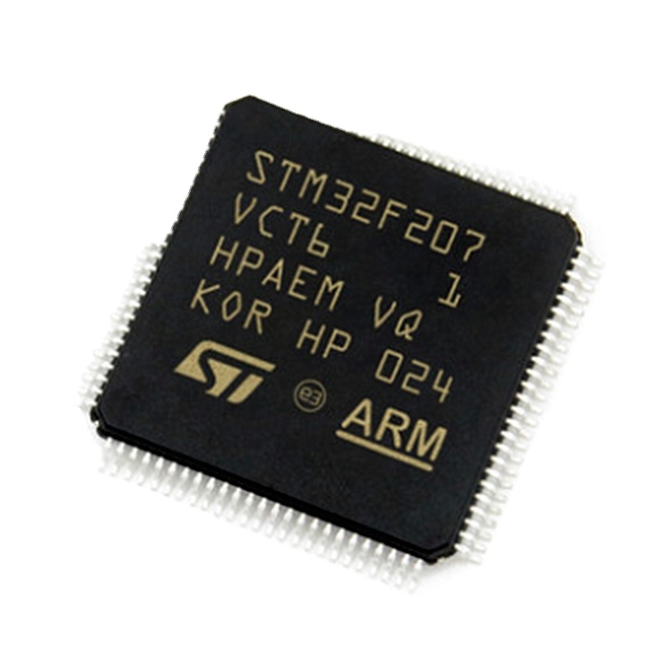
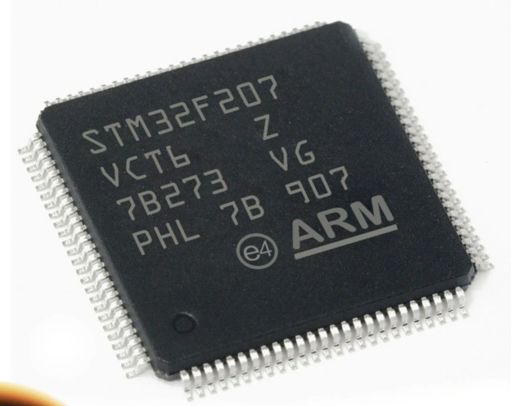
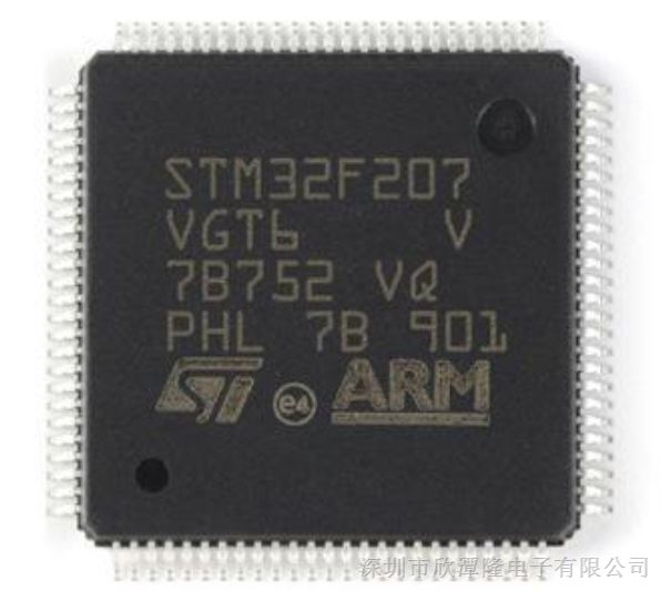
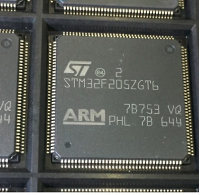
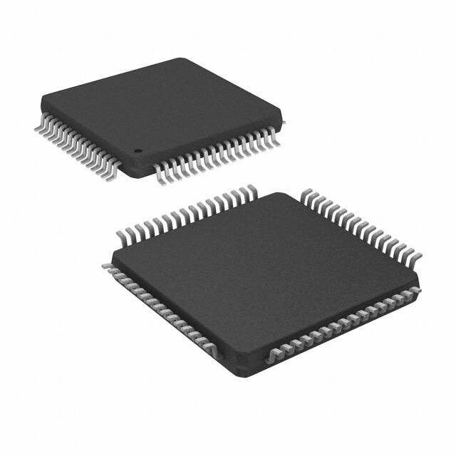
 Reverse Secured STM32F207VCT6 Microprocessor Flash Heximal
Reverse Secured STM32F207VCT6 Microprocessor Flash Heximal and dump embedded firmware from stm32f207vct6 flash memory, extract source code from stm32f207vct6 flash memory;
Reverse Secured STM32F207VCT6 Microprocessor Flash Heximal and dump embedded firmware from stm32f207vct6 flash memory, extract source code from stm32f207vct6 flash memory;
Peripheral available only on STM32F207xx devices.
The STM32F207xx devices provide an IEEE-802.3-2002-compliant media access controller (MAC) for Ethernet LAN communications through an industry-standard medium- independent interface (MII) or a reduced medium-independent interface (RMII).
The STM32F207xx requires an external physical interface device (PHY) to connect to the physical LAN bus (twisted-pair, fiber, etc.). the PHY is connected to the STM32F207xx MII port using 17 signals for MII or 9 signals for RMII, and can be clocked using the 25 MHz (MII) or 50 MHz (RMII) output from the STM32F207xx by restoring stm32f205zct6 locked mcu chip memory content.
obrnuti inženjer osigurao STM32F207VCT6 mikroprocesorski sustav otpora neovlaštenog mijenjanja i program za flash memoriju za očitavanje i softver iz otključanog mikrokontrolera STM32F207VCT6 kopirati ugrađeni firmware izvornog koda na novi STM32F207VCT6 zaštitni MCU čip,
The STM32F207xx includes the following features:
Supports 10 and 100 Mbit/s rates
Dedicated DMA controller allowing high-speed transfers between the dedicated SRAM and the descriptors (see the STM32F20x and STM32F21x reference manual for details)
Tagged MAC frame support (VLAN support)
Half-duplex (CSMA/CD) and full-duplex operation
MAC control sublayer (control frames) support
32-bit CRC generation and removal
inżynieria wsteczna zabezpieczony STM32F207VCT6 mikroprocesorowy system odporności na manipulacje oraz odczyt programu pamięci flash i oprogramowania z odblokowanego mikrokontrolera STM32F207VCT6 kopiowania wbudowanego oprogramowania układowego kodu źródłowego do nowego STM32F207VCT6 ochronnego układu MCU,
Several address filtering modes for physical and multicast address (multicast and group addresses)
32-bit status code for each transmitted or received frame
Internal FIFOs to buffer transmit and receive The transmit FIFO and the receive FIFO are both 2 Kbytes (4 Kbytes in total)
Supports hardware PTP (precision time protocol) in accordance with IEEE 1588 2008 (PTP V2) with the time stamp comparator connected to the TIM2 input
Triggers interrupt when system time becomes greater than target time
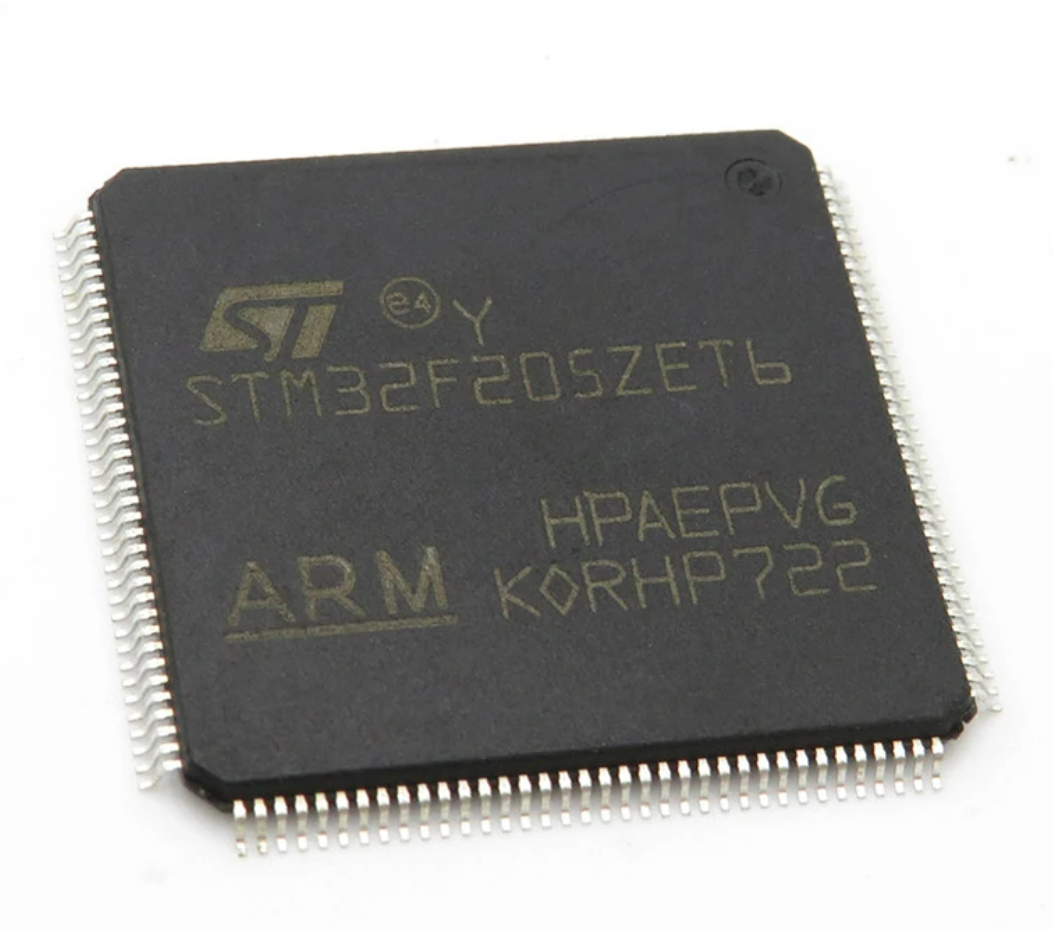
Reverse Secured STM32F205ZGT6 MCU Flash Program
Reverse Secured STM32F205ZGT6 MCU Flash Program means the embedded heximal file can be readout directly from STM32F205ZGT6 Microcontroller flash memory, decrypt arm microprocessor stm32f205zgt6 memory file;
Reverse Secured STM32F205ZGT6 MCU Flash Program means the embedded heximal file can be readout directly from STM32F205ZGT6 Microcontroller flash memory, decrypt arm microprocessor stm32f205zgt6 memory file
The VBAT pin allows to power the device VBAT domain from an external battery or an external supercapacitor.
VBAT operation is activated when VDD is not present.
The VBAT pin supplies the RTC, the backup registers and the backup SRAM.
Note:
When the microcontroller is supplied from VBAT, external interrupts and RTC alarm/events do not exit it from VBAT operation.
When using WLCSP64+2 package, if IRROFF pin is connected to VDD, the VBAT
functionality is no more available and VBAT pin must be connected to VDD by recover arm microcontroller stm32f205rg flash code.
The STM32F20x devices include two advanced-control timers, eight general-purpose timers, two basic timers and two watchdog timers.
All timer counters can be frozen in debug mode.
Table 5 compares the features of the advanced-control, general-purpose and basic timers
decode stm32f205zgt6 mcu embedded heximal and copy firmware to new microcontroller
The advanced-control timers (TIM1, TIM8) can be seen as three-phase PWM generators multiplexed on 6 channels. They have complementary PWM outputs with programmable inserted dead times. They can also be considered as complete general-purpose timers. Their 4 independent channels can be used for:
- Input capture
- Output compare
- PWM generation (edge- or center-aligned modes)
- One-pulse mode output
If configured as standard 16-bit timers, they have the same features as the general-purpose TIMx timers. If configured as 16-bit PWM generators, they have full modulation capability (0- 100%) in the process of attacking stm32f205vb mcu protective fuse bit.
The TIM1 and TIM8 counters can be frozen in debug mode. Many of the advanced-control timer features are shared with those of the standard TIMx timers which have the same architecture. The advanced-control timer can therefore work together with the TIMx timers via the Timer Link feature for synchronization or event chaining.
Reverse Engineering STM32F205ZE Microcontroller Heximal Code
Reverse Engineering STM32F205ZET6 Microcontroller Heximal Code and readout embedded heximal file from STM32F205ZET6 MCU flash memory, copy firmware to new Microprocessor stm32f205zet6;
Reverse Engineering STM32F205ZET6 Microcontroller Heximal Code and readout embedded heximal file from STM32F205ZET6 MCU flash memory, copy firmware to new Microprocessor stm32f205zet6
The device remains in reset mode when VDD is below a specified threshold, VPOR/PDR or VBOR, without the need for an external reset circuit. On devices in WLCSP64+2 package, the BOR, POR and PDR features can be disabled by setting IRROFF pin to VDD. In this mode an external power supply supervisor is required (see Section 3.16).
The devices also feature an embedded programmable voltage detector (PVD) that monitors the VDD/VDDA power supply and compares it to the VPVD threshold. An interrupt can be generated when VDD/VDDA drops below the VPVD threshold and/or when VDD/VDDA is higher than the VPVD threshold. The interrupt service routine can then generate a warning message and/or put the MCU into a safe state. The PVD is enabled by software.
Código heximal del microcontrolador STM32F205ZET6 de ingeniería inversa y lectura del archivo heximal integrado de la memoria flash MCU STM32F205ZET6, copia del firmware al nuevo microprocesador stm32f205zet6
The regulator ON modes are activated by default on LQFP packages.On WLCSP64+2 package, they are activated by connecting both REGOFF and IRROFF pins to VSS, while only REGOFF must be connected to VSS on UFBGA176 package (IRROFF is not available).
VDD minimum value is 1.8 V.
break arm controller stm32f205zet6 fuse bit and extract embedded heximal file from mcu chip’s flash memory
There are three power modes configured by software when the regulator is ON:
- MR is used in the nominal regulation mode
- LPR is used in Stop modes
The LP regulator mode is configured by software when entering Stop mode.
- Power-down is used in Standby
The Power-down mode is activated only when entering Standby mode. The regulator output is in high impedance and the kernel circuitry is powered down, inducing zero consumption. The contents of the registers and SRAM are lost).
Two external ceramic capacitors must be connected on VCAP_1 and VCAP_2 pin. Refer to
Figure 19: Power supply scheme and Table 16: VCAP1/VCAP2 operating conditions.
All packages have the regulator ON feature.
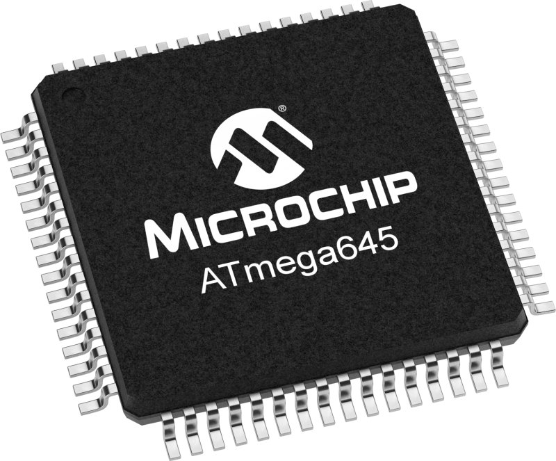
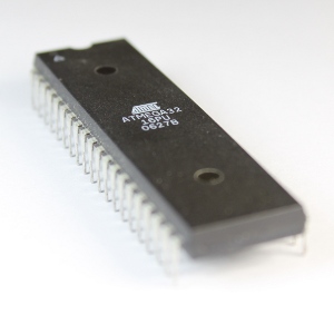
Reverse Protected ATMEGA645 MCU Heximal
Reverse Protected ATMEGA645 MCU Heximal is a process to readout chip atmega645 firmware from its flash and eeprom after attack locked microcontroller atmega645 protective system;
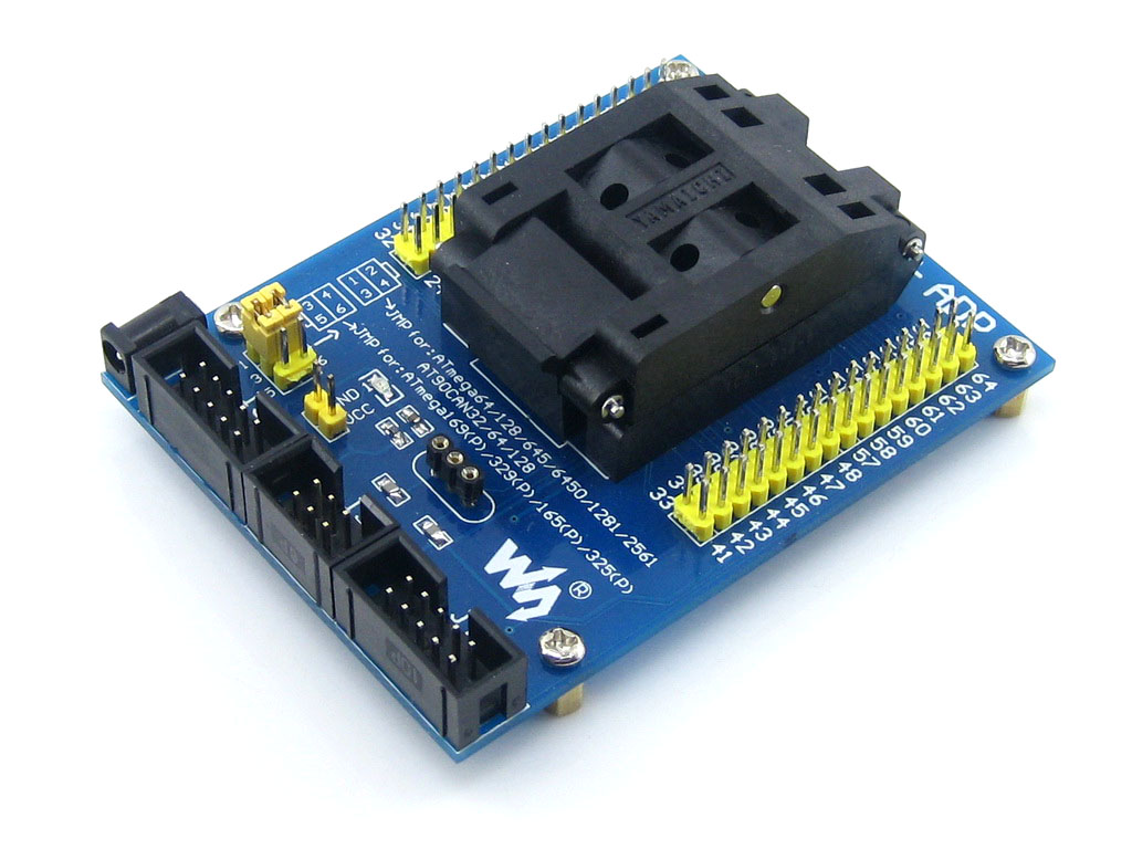
Reverse Protected ATMEGA645 MCU Heximal is a process to readout chip atmega645 firmware from its flash and eeprom after attack locked microcontroller atmega645 protective system
Atmel offers the QTouch® library for embedding capacitive touch buttons, sliders and wheels- functionality into AVR microcontrollers. The patented charge-transfer signal acquisition offersrobust sensing and includes fully debounced reporting of touch keys and includes Adjacent KeySuppression® (AKS™) technology for unambiguous detection of key events to copy chip atmega645 mcu file. The easy-to-use QTouch Suite toolchain allows you to explore, develop and debug your own touch applications.
atmega645 mcu protegido inversamente heximal es un proceso para leer el firmware del chip atmega645 desde su flash y eeprom después de un ataque bloqueado sistema de protección del microcontrolador atmega645;
The device is manufactured using Atmel’s high density non-volatile memory technology. The On-chip In-System re-Programmable (ISP) Flash allows the program memory to be repro- grammed In-System through an SPI serial interface, by a conventional non-volatile memory programmer, or by an On-chip Boot program running on the AVR core. The Boot program can use any interface to download the application program in the Application Flash memory.
decode secured mcu chip atmega645 flash memory and copy its binary
Software in the Boot Flash section will continue to run while the Application Flash section is updated, providing true Read-While-Write operation. By combining an 8-bit RISC CPU with In-System Self-Programmable Flash on a monolithic chip, the Atmel Atmel ATmega645 is a powerful microcontroller that provides a highly flexible and cost effective solution to many embedded control applications.
The Atmel ATmega325/3250/645/6450 is supported with a full suite of program and system development tools including: C Compilers, Macro Assemblers, Program Debugger/Simulators, In-Circuit Emulators, and Evaluation kits.
Reverse Engineer DSP TMS320F28030PAG Microcontroller Flash Memory
Reverse Engineer DSP TMS320F28030PAG Microcontroller Flash Memory and restore dsp cpu tms320f28030pagt source code, copy flash program to new tms320f28030pag texas instrument dsp mcu;
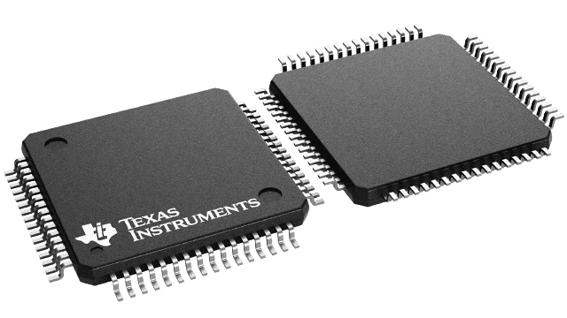
Reverse Engineer DSP TMS320F28030PAG Microcontroller Flash Memory and restore dsp cpu tms320f28030pagt source code, copy flash program to new tms320f28030pag texas instrument dsp mcu
Section 6.2.1 describes the signals. With the exception of the JTAG pins, the GPIO function is the default at reset, unless otherwise mentioned. The peripheral signals that are listed under them are alternate functions. Some peripheral functions may not be available in all devices. See Table 5-1 for details. Inputs are not 5-V tolerant. All GPIO pins are I/O/Z and have an internal pullup, which can be selectively enabled/disabled on a per-pin basis. This feature only applies to the GPIO pins. The pullups on the PWM pins are not enabled at reset. The pullups on other GPIO pins are enabled upon reset. The AIO pins do not have an internal pullup.
memoria flash del microcontrolador DSP TMS320F28030PAG de ingeniería inversa y restauración del código fuente dsp cpu tms320f28030pagt, copia del programa flash al nuevo instrumento tms320f28030pag texas dsp mcu;
When the on-chip VREG is used, the GPIO19, GPIO34, GPIO35, GPIO36, GPIO37, and GPIO38 pins could glitch during power up. This potential glitch will finish before the boot mode pins are read and will not affect boot behavior. If glitching is unacceptable in an application, 1.8 V could be supplied externally.
attack tms320f28030pag dsp mcu protection and restore flash memory binary program
Alternatively, adding a current-limiting resistor (for example, 470 Ω) in series with these pins and any external driver could be considered to limit the potential for degradation to the pin and/or external circuitry. There is no power-sequencing requirement when using an external 1.8-V supply. However, if the 3.3-V transistors in the level-shifting output buffers of the I/O pins are powered before the 1.8-V transistors, it is possible for the output buffers to turn on, causing a glitch to occur on the pin during power up. To avoid this behavior, power the VDD pins before or with the VDDIO pins, ensuring that the VDD pins have reached 0.7 V before the VDDIO pins reach 0.7 V.
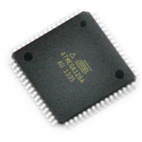
Encrypted ATMEL ATMEGA128A MCU Flash Decoding
Encrypted ATMEL ATMEGA128A MCU Flash Decoding will help engineer to copy atmega128a microcontroller flash heximal file out after readout atmega128a microprocessor’s content software from its flash and eeprom memory;
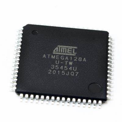
Encrypted ATMEL ATMEGA128A MCU Flash Decoding will help engineer to copy atmega128a microcontroller flash heximal file out after readout atmega128a microprocessor’s content software from its flash and eeprom memory
In this mode, the Watchdog Timer is always enabled, and the WDE bit will always read as one. A timed sequence is needed when changing the Watchdog Time-out period. To change the Watchdog Time-out, the following procedure must be followed:
- In the same operation, write a logical one to WDCE and WDE. Even though the WDE always is set, the WDE must be written to one to start the timed sequence
Within the next four clock cycles, in the same operation, write the WDP bits as desired, but with the WDCE bit cleared. The value written to the WDE bit is irrelevant to break atmega128a mcu fuse bit inside the flash memory.
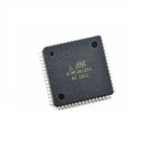
La decodificación flash MCU ATMEL ATMEGA128A cifrada ayudará al ingeniero a copiar el archivo heximal flash del microcontrolador atmega128a después de leer el software de contenido del microprocesador atmega128a de su memoria flash y eeprom
This section describes the specifics of the interrupt handling performed by the ATmega8. For a general explanation of the AVR interrupt handling, refer to “Reset and Interrupt Handling” on page 14.
Table 19 on page 47 shows reset and Interrupt Vectors placement for the various combinations of BOOTRST and IVSEL settings. If the program never enables an interrupt source, the Interrupt Vectors are not used, and regular program code can be placed at these locations. This is also the case if the Reset Vector is in the Application section while the Interrupt Vectors are in the boot section or vice versa to break atmega128a ic chip flash memory.
attack atmega128a microcontroller fuse bit and extract atmega128a source code
- When the BOOTRST Fuse is programmed, the device will jump to the Boot Loader address at reset, see “Boot Loader Support – Read-While-Write Self-Programming” on page 202
- When the IVSEL bit in GICR is set, Interrupt Vectors will be moved to the start of the boot Flash The address of each Interrupt Vector will then be the address in this table added to the start address of the boot Flash section;
- The Boot Reset Address is shown in Table 82 on page 213. For the BOOTRST Fuse “1” means unprogrammed while “0” means programmed
The most typical and general program setup for the Reset and Interrupt Vector Addresses in ATmega128A is:
| addressLabels | Code | Comments | ||
| $000 | rjmp | RESET | ; Reset Handler | |
| $001 | rjmp | EXT_INT0 | ; IRQ0 Handler | |
| $002 | rjmp | EXT_INT1 | ; IRQ1 Handler | |
| $003 | rjmp | TIM2_COMP | ; Timer2 Compare Handler | |
| $004 | rjmp | TIM2_OVF | ; Timer2 Overflow Handler | |
| $005 | rjmp | TIM1_CAPT | ; Timer1 Capture Handler | |
| $006 | rjmp | TIM1_COMPA | ; Timer1 CompareA Handler | |
| $007 | rjmp | TIM1_COMPB | ; Timer1 CompareB Handler | |
| $008 | rjmp | TIM1_OVF | ; Timer1 Overflow Handler | |
| $009 | rjmp | TIM0_OVF | ; Timer0 Overflow Handler | |
| $00a | rjmp | SPI_STC | ; SPI Transfer Complete Handler | |
| $00b | rjmp | USART_RXC | ; USART RX Complete Handler | |
| $00c | rjmp | USART_UDRE | ; UDR Empty Handler | |
| $00d | rjmp | USART_TXC | ; USART TX Complete Handler | |
| $00e | rjmp | ADC | ; ADC Conversion Complete Handler | |
| $00f | rjmp | EE_RDY | ; EEPROM Ready Handler | |
| $010 | rjmp | ANA_COMP | ; Analog Comparator Handler | |
| $011 | rjmp | TWSI | ; Two-wire Serial Interface Handler | |
| $012 | rjmp | SPM_RDY | ; Store Program Memory Ready Handler | |
| ; | ||||
| $013 | RESET: ldi | r16,high(RAMEND); Main program start | ||
| $014 | out | SPH,r16 ; Set Stack Pointer to top of RAM | ||
| $015 | ldi | r16,low(RAMEND) | ||
| $016 | out | SPL,r16 | ||
| $017 | sei | ; Enable interrupts | ||
| $018 | <instr> xxx | |||
| … | … | … | ||
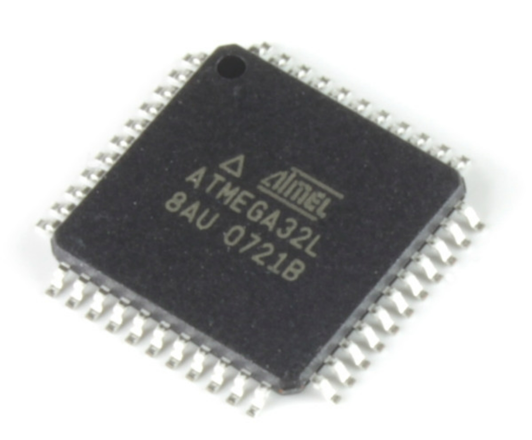
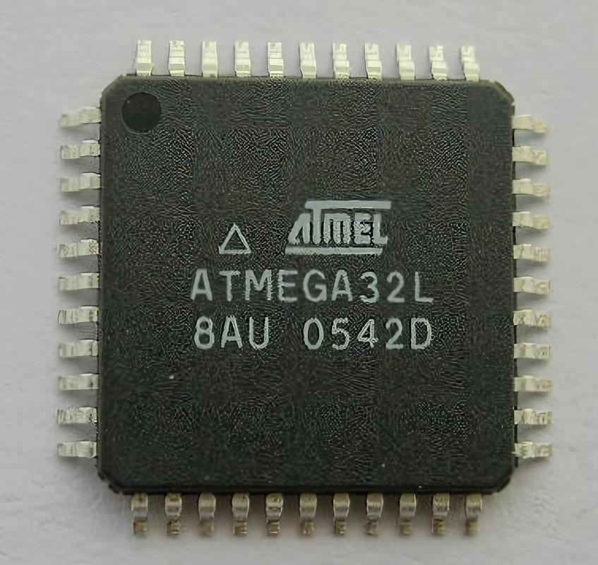
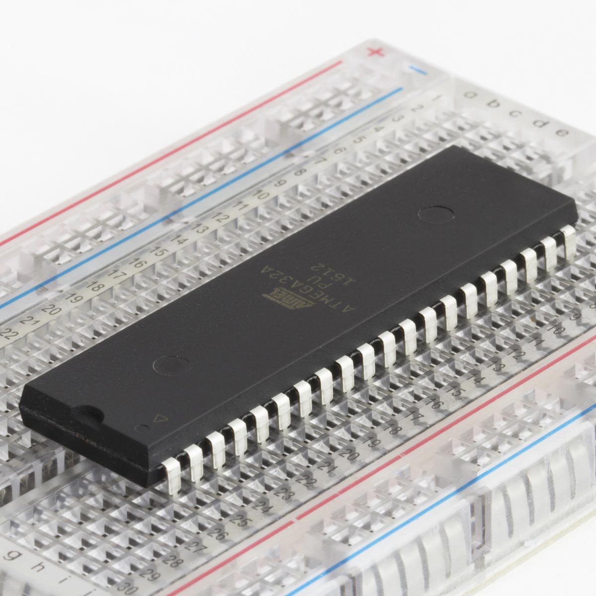
Reverse Engineer AVR Chip ATMEGA32L Microcontroller
Reverse Engineer AVR Chip ATMEGA32L Microcontroller flash memory protection system is a process to crack mcu atmega32l flash memory fuse bit and readout heximal software from atmega32l mcu flash memory;
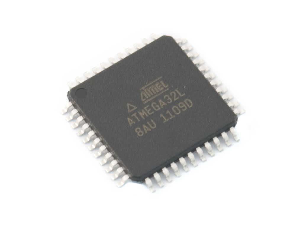
Reverse Engineer AVR Chip ATMEGA32L Microcontroller flash memory protection system is a process to crack mcu atmega32l flash memory fuse bit and readout heximal software from atmega32l mcu flash memory
XTAL1 and XTAL2 are input and output, respectively, of an inverting amplifier which can be con- figured for use as an On-chip Oscillator, as shown in Figure 11. Either a quartz crystal or a ceramic resonator may be used. The CKOPT Fuse selects between two different Oscillator amplifier modes.
When CKOPT is programmed, the Oscillator output will oscillate a full rail-to- rail swing on the output. This mode is suitable when operating in a very noisy environment or when the output from XTAL2 drives a second clock buffer to restore atmega32l mcu flash memory code. This mode has a wide frequency range. When CKOPT is unprogrammed, the Oscillator has a smaller output swing.
ingeniería inversa AVR chip ATMEGA32L microcontrolador sistema de protección de memoria flash es un proceso para romper mcu atmega32l memoria flash fusible bit y lectura de software heximal de atmega32l mcu memoria flash;
This reduces power consumption considerably. This mode has a limited frequency range and it cannot be used to drive other clock buffers. For resonators, the maximum frequency is 8MHz with CKOPT unprogrammed and 16MHz with CKOPT programmed. C1 and C2 should always be equal for both crystals and resonators.
break atmega32l mcu chip flash lock and recover flash memory program data
The optimal value of the capacitors depends on the crystal or resonator in use, the amount of stray capacitance, and the electromagnetic noise of the environment to break atmega32l mcu encryption fuse bit. Some initial guidelines for choosing capacitors for use with crystals are given in Table 4. For ceramic resonators, the capacitor values given by the manufacturer should be used.
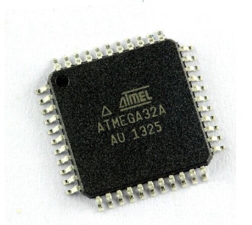
Reverse ATMEL AVR MCU ATmega32A Heximal Code
Reverse ATMEL AVR MCU ATmega32A Heximal Code is a process to unlock atmega32a locked microcontroller fuse bit and read embedded firmware out from atmega32a avr chip flash memory;
crack avr mcu atmega32a protection and copy heximal file
The AVR Stack Pointer is implemented as two 8-bit registers in the I/O space. The number of bits actually used is implementation dependent. Note that the data space in some implementations of the AVR architecture is so small that only SPL is needed. In this case, the SPH Register will not be present.
This section describes the general access timing concepts for instruction execution. The Atmel®AVR® CPU is driven by the CPU clock clkCPU, directly generated from the selected clock source for the chip. No internal clock division is used.
revertir ATMEL AVR MCU ATmega32A código heximal es un proceso para desbloquear atmega32a microcontrolador bloqueado bit fusible y leer el firmware embebido a cabo a partir de atmega32a avr chip de memoria flash
Figure 5 shows the parallel instruction fetches and instruction executions enabled by the Harvard architecture and the fast-access Register File concept. This is the basic pipe-lining concept to obtain up to 1 MIPS per MHz with the corresponding unique results for functions per cost, functions per clocks, and functions per power-unit to copy avr mcu atmega32a software.
Figure 6 shows the internal timing concept for the Register File. In a single clock cycle an ALU operation using two register operands is executed, and the result is stored back to the destination register.
Reverse ATMEL AVR MCU ATmega32A Heximal Code is a process to unlock atmega32a locked microcontroller fuse bit and read embedded firmware out from atmega32a avr chip flash memory
The Atmel®AVR® provides several different interrupt sources. These interrupts and the separate Reset Vector each have a separate Program Vector in the Program memory space. All interrupts are assigned individual enable bits which must be written logic one together with the Global Interrupt Enable bit in the Status Register in order to enable the interrupt by breaking of avr microcontroller atmega32a protection fuse bit.
Depending on the Program Counter value, interrupts may be automatically disabled when Boot Lock Bits BLB02 or BLB12 are programmed. This feature improves software security. See the section “Memory Programming” on page 215 for details.
Crack Secured Microcontroller PIC12LF1612 Protection
Crack Secured Microcontroller PIC12LF1612 Protection and extract embedded binary file from PIC12F617 MCU;
Crack Secured Microcontroller PIC12LF1612 Proteção e extração de arquivo binário embutido do PIC12F617 MCU
Because the OSCCON register is cleared on Reset events, the INTOSC (or postscaler) clock source is not initially available after a Reset event; the INTRC clock is used directly at its base frequency. To use a higher clock speed on wake-up, the INTOSC or postscaler clock sources can be selected to provide a higher clock speed by setting bits, IFRC2:IFRC0, immediately after Reset. For wake-ups from Sleep, the INTOSC or post- scaler clock sources can be selected by setting IFRC2:IFRC0 prior to entering Sleep mode.
Взлом защищенного микроконтроллера PIC12LF1612 Защита и извлечение встроенного бинарного файла из микроконтроллера PIC12F617
In all other power managed modes, Two-Speed Start-up is not used. The device will be clocked by the currently selected clock source until the primary clock source becomes available. The setting of the IESO bit is ignored to unlock microchip pic12f615 flash memory.
While using the INTRC oscillator in Two-Speed Start- up, the device still obeys the normal command sequences for entering power managed modes, including serial SLEEP instructions (refer to Section 3.1.3 “Multiple Sleep Commands”). In practice, this means that user code can change the SCS1:SCS0 bit settings and issue SLEEP commands before the OST times out.
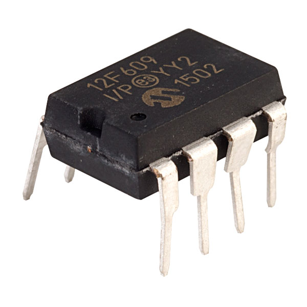
Microchip PIC12F609 Processor Flash Binary Duplication
Microchip PIC12F609 Processor Flash Binary Duplication can help engineer to unlock microcontroller pic12f609 heximal, and copy embedded firmware to new microprocessor pic12f609;
La duplicación binaria flash del procesador PIC12F609 de Microchip puede ayudar al ingeniero a desbloquear el microcontrolador pic12f609 heximal y copiar el firmware incorporado al nuevo microprocesador pic12f609
Depending on the power source for the device voltage, the voltage normally decreases relatively slowly. This means that the LVD module does not need to be constantly operating when breaking off pic12f615 mcu software. To decrease the current require- ments, the LVD circuitry only needs to be enabled for short periods, where the voltage is checked. After doing the check, the LVD module may be disabled.
Each time that the LVD module is enabled, the circuitry requires some time to stabilize. After the circuitry has stabilized, all status flags may be cleared in the process of breaking pic12f609 ic chip flash memory. The module will then indicate the proper state of the system.
Ataque el microcontrolador PIC12F609 bloqueado y deshabilite el bit de fusible de seguridad, restaure el archivo heximal en la memoria flash MCU PIC12F609;
The following steps are needed to set up the LVD module:
- Write the value to the LVDL3:LVDL0 bits (LVDCON register), which selects the desired LVD trip
- Ensure that LVD interrupts are disabled (the LVDIE bit is cleared or the GIE bit is cleared).
- Enable the LVD module (set the LVDEN bit in the LVDCON register).
- Wait for the LVD module to stabilize (the IRVST bit to become set).
- Clear the LVD interrupt flag, which may have falsely become set, until the LVD module has stabilized (clear the LVDIF bit).
- Enable the LVD interrupt (set the LVDIE and the GIE bits).