Posts Tagged ‘Обратный инжиниринг DSP TMS320F28030PAG Флэш-память микроконтроллера’
 Reverse Engineer DSP TMS320F28030PAG Microcontroller Flash Memory
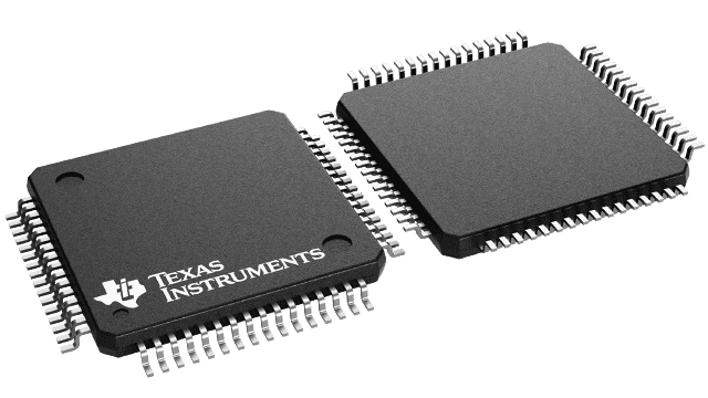
Reverse Engineer DSP TMS320F28030PAG Microcontroller Flash Memory and restore dsp cpu tms320f28030pagt source code, copy flash program to new tms320f28030pag texas instrument dsp mcu;
Reverse Engineer DSP TMS320F28030PAG Microcontroller Flash Memory and restore dsp cpu tms320f28030pagt source code, copy flash program to new tms320f28030pag texas instrument dsp mcu
Section 6.2.1 describes the signals. With the exception of the JTAG pins, the GPIO function is the default at reset, unless otherwise mentioned. The peripheral signals that are listed under them are alternate functions. Some peripheral functions may not be available in all devices. See Table 5-1 for details. Inputs are not 5-V tolerant. All GPIO pins are I/O/Z and have an internal pullup, which can be selectively enabled/disabled on a per-pin basis. This feature only applies to the GPIO pins. The pullups on the PWM pins are not enabled at reset. The pullups on other GPIO pins are enabled upon reset. The AIO pins do not have an internal pullup.
memoria flash del microcontrolador DSP TMS320F28030PAG de ingeniería inversa y restauración del código fuente dsp cpu tms320f28030pagt, copia del programa flash al nuevo instrumento tms320f28030pag texas dsp mcu;
When the on-chip VREG is used, the GPIO19, GPIO34, GPIO35, GPIO36, GPIO37, and GPIO38 pins could glitch during power up. This potential glitch will finish before the boot mode pins are read and will not affect boot behavior. If glitching is unacceptable in an application, 1.8 V could be supplied externally.
attack tms320f28030pag dsp mcu protection and restore flash memory binary program
Alternatively, adding a current-limiting resistor (for example, 470 Ω) in series with these pins and any external driver could be considered to limit the potential for degradation to the pin and/or external circuitry. There is no power-sequencing requirement when using an external 1.8-V supply. However, if the 3.3-V transistors in the level-shifting output buffers of the I/O pins are powered before the 1.8-V transistors, it is possible for the output buffers to turn on, causing a glitch to occur on the pin during power up. To avoid this behavior, power the VDD pins before or with the VDDIO pins, ensuring that the VDD pins have reached 0.7 V before the VDDIO pins reach 0.7 V.