Archive for the ‘Reverse Engineer Microcontroller’ Category
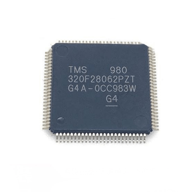
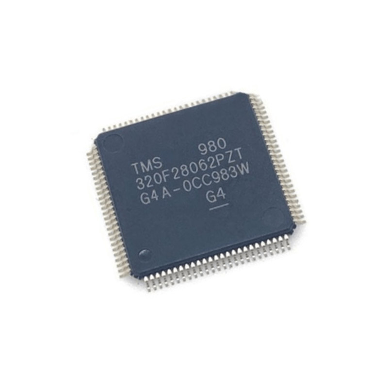
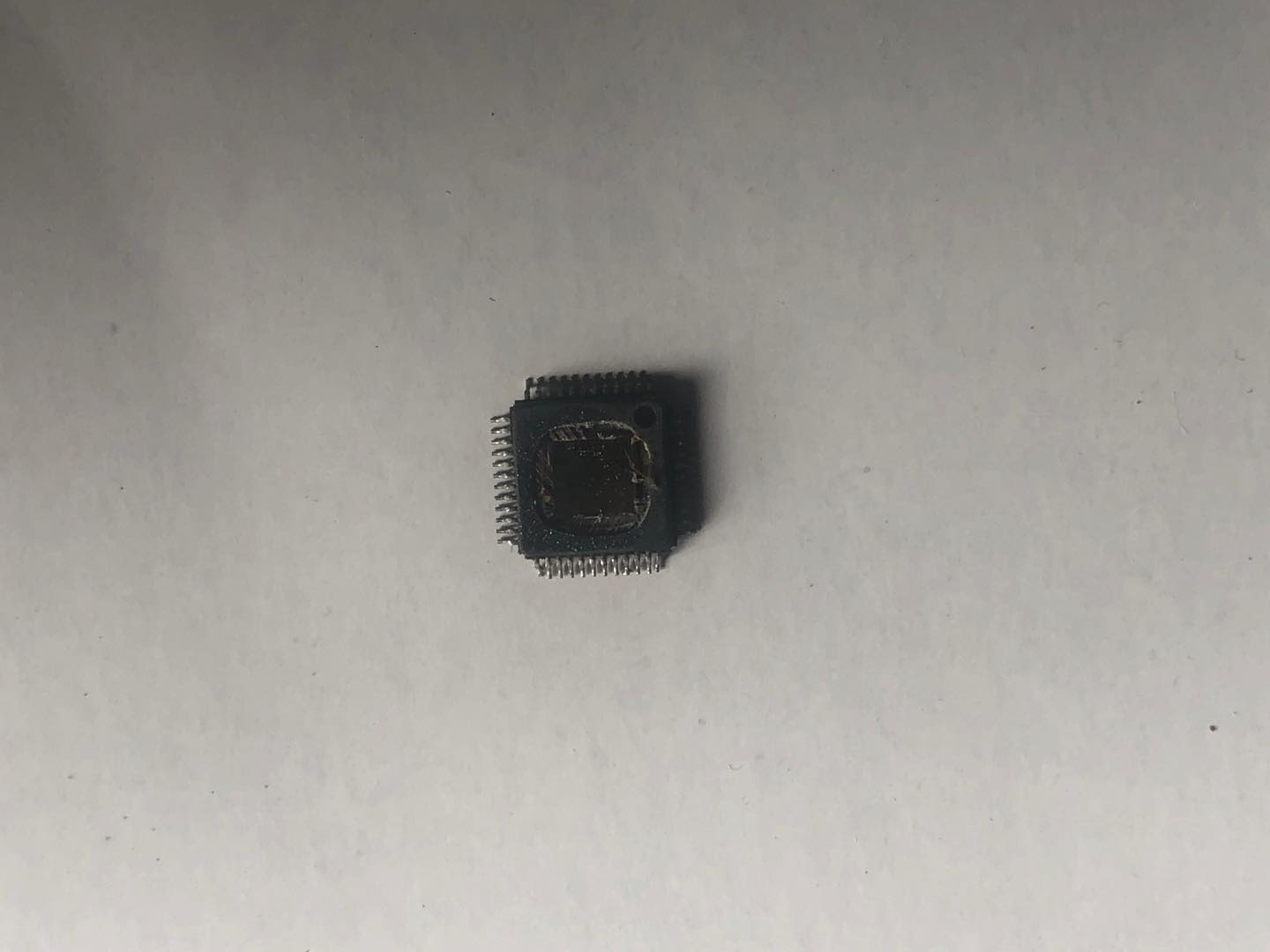
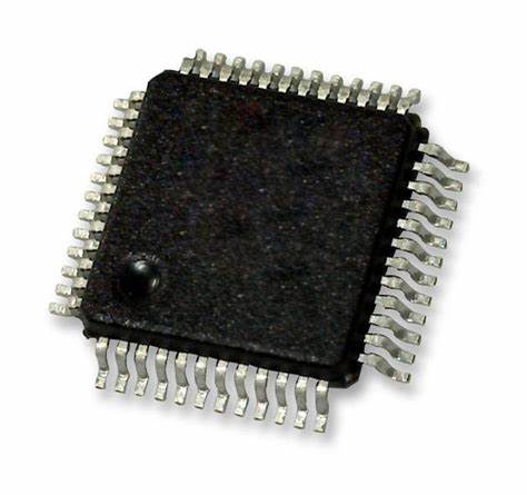
 Reverse DSP MCU TMS320F28062PZT Flash Firmware
Reverse DSP MCU TMS320F28062PZT Flash Firmware is a process to unlock dsp microcontroller tms320f28062 encryption over its flash memory, and then the binary code will be readout from microprocessor tms320f28062pzt flash memory;
Reverse DSP MCU TMS320F28062PZT Flash Firmware is a process to unlock dsp microcontroller tms320f28062 encryption over its flash memory, and then the binary code will be readout from microprocessor tms320f28062pzt flash memory
The peripheral – I/O multiplexing implemented in the device prevents all available peripherals from being used at the same time. This is because more than one peripheral function may share an I/O pin. It is, however, possible to turn on the clocks to all the peripherals at the same time, although such a configuration is not useful. If this is done, the current drawn by the device will be more than the numbers specified in the current consumption tables.
The 2803x devices incorporate a method to reduce the device current consumption. Because each peripheral unit has an individual clock-enable bit, significant reduction in current consumption can be achieved by turning off the clock to any peripheral module that is not used in a given application. Furthermore, any one of the three low-power modes could be taken advantage of to reduce the current consumption even further. Table 7-1 indicates the typical reduction in current consumption achieved by turning off the clocks.
All peripheral clocks (except CPU Timer clock) are disabled upon reset. Writing to/reading from peripheral registers is possible only after the peripheral clocks are turned; This number represents the current drawn by the digital portion of the ADC module. Turning off the clock to the ADC module results in the elimination of the current drawn by the analog portion of the ADC (IDDA) as well.
Обратное прошивка DSP MCU TMS320F28062PZT Flash — это процесс разблокировки шифрования микроконтроллера tms320f28062 dsp через его флэш-память, после чего двоичный код будет считан из флэш-памяти микропроцессора tms320f28062pzt.
For peripherals with multiple instances, the current quoted is per For example, the 2 mA value quoted for ePWM is for one ePWM module.The baseline IDD current (current when the core is executing a dummy loop with no peripherals enabled) is 40 mA, typical. To arrive at the IDD current for a given application, the current-drawn by the peripherals (enabled by that application) must be added to the baseline IDD current.
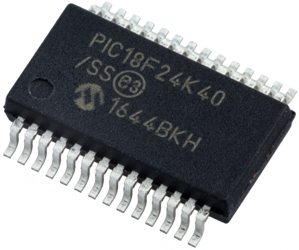
Reverse Engineering PIC18F24K40T Microcontroller Heximal Data
Reverse Engineering PIC18F24K40T Microcontroller Heximal Data is a process to crack pic18f24k40t mcu security fuse bit, and then readout secured code from microprocessor pic18f24k40t flash memory;
The PIC18F24K40T devices contain circuitry to prevent clocking “glitches” when switching between clock sources. A short pause in the system clock occurs during the clock switch.
The length of this pause is between eight and nine clock periods of the new clock source. This ensures that the new clock source is stable and that its pulse width will not be less than the shortest pulse width of the two clock sources.
When the device executes a SLEEP instruction, the system is switched to one of the power managed modes, depending on the state of the IDLEN and SCS1:SCS0 bits of the OSCCON register when recover microcontroller pic18f24k20 flash program and eeprom data.
ingeniería inversa PIC18F24K40T microcontrolador de datos heximales es un proceso para romper pic18f24k40t mcu fusible de seguridad de bits, y luego leer el código de seguridad del microprocesador pic18f24k40t memoria flash
When PRI_IDLE mode is selected, the designated primary oscillator continues to run without interruption. For all other power managed modes, the oscillator using the OSC1 pin is disabled. The OSC1 pin (and OSC2 pin, if used by the oscillator) will stop oscillating.
In Secondary Clock modes (SEC_RUN and SEC_I- DLE), the Timer1 oscillator is operating and providing the system clock in the process of pic18f24k22 mcu locked code recovery. The Timer1 oscillator may also run in all power managed modes if required to clock Timer1 or Timer3.
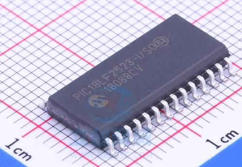
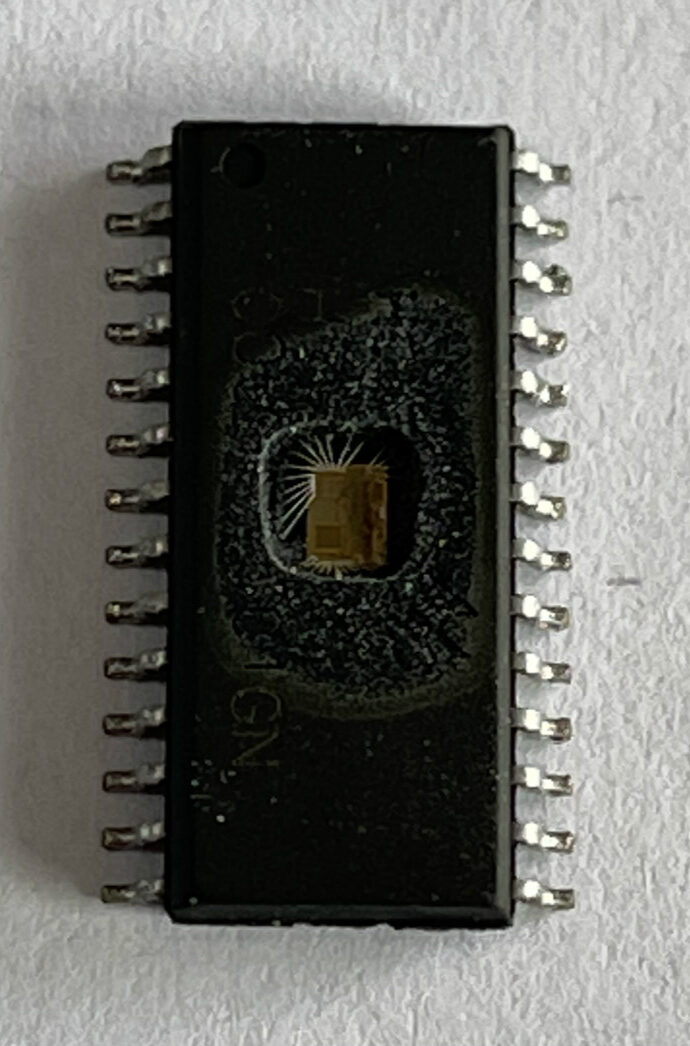
Reverse PIC18LF2523 Microchip MCU Flash Memory
Reverse PIC18LF2523 Microchip MCU Flash Memory and extract embedded program from microcontroller pic18lf2523 in the format of heximal, the original binary file of pic18lf2523 secured processor will be copied;
In the RC Oscillator mode, the oscillator frequency divided by 4 is available on the OSC2 pin. This signal may be used for test purposes, or to synchronize other logic.
The RCIO Oscillator mode functions like the RC mode, except that the OSC2 pin becomes an additional general purpose I/O pin. The I/O pin becomes bit 6 of PORTA (RA6) is a process of decoding microcontroller pic18f1220 flash program.
The PIC18LF2523 devices include an internal oscillator block, which generates two different clock signals; either can be used as the system’s clock source. This can eliminate the need for external oscillator circuits on the OSC1 and/or OSC2 pins.
invertir PIC18LF2523 microchip MCU memoria flash y extraer el programa incrustado del microcontrolador pic18lf2523 en el formato de heximal, se copiará el archivo binario original del procesador seguro pic18lf2523
The main output (INTOSC) is an 8 MHz clock source, which can be used to directly drive the system clock. It also drives a postscaler, which can provide a range of clock frequencies from 125 kHz to 4 MHz when decapsulate pic18f1320 processor silicon package. The INTOSC output is enabled when a system clock frequency from 125 kHz to 8 MHz is selected.
The other clock source is the internal RC oscillator (INTRC), which provides a 31 kHz output. The INTRC oscillator is enabled by selecting the internal oscillator block as the system clock source, or when any of the following are enabled:
- Power-up Timer
- Fail-Safe Clock Monitor
- Watchdog Timer
- Two-Speed Start-up
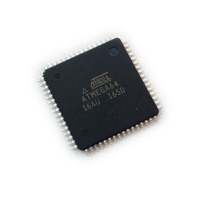
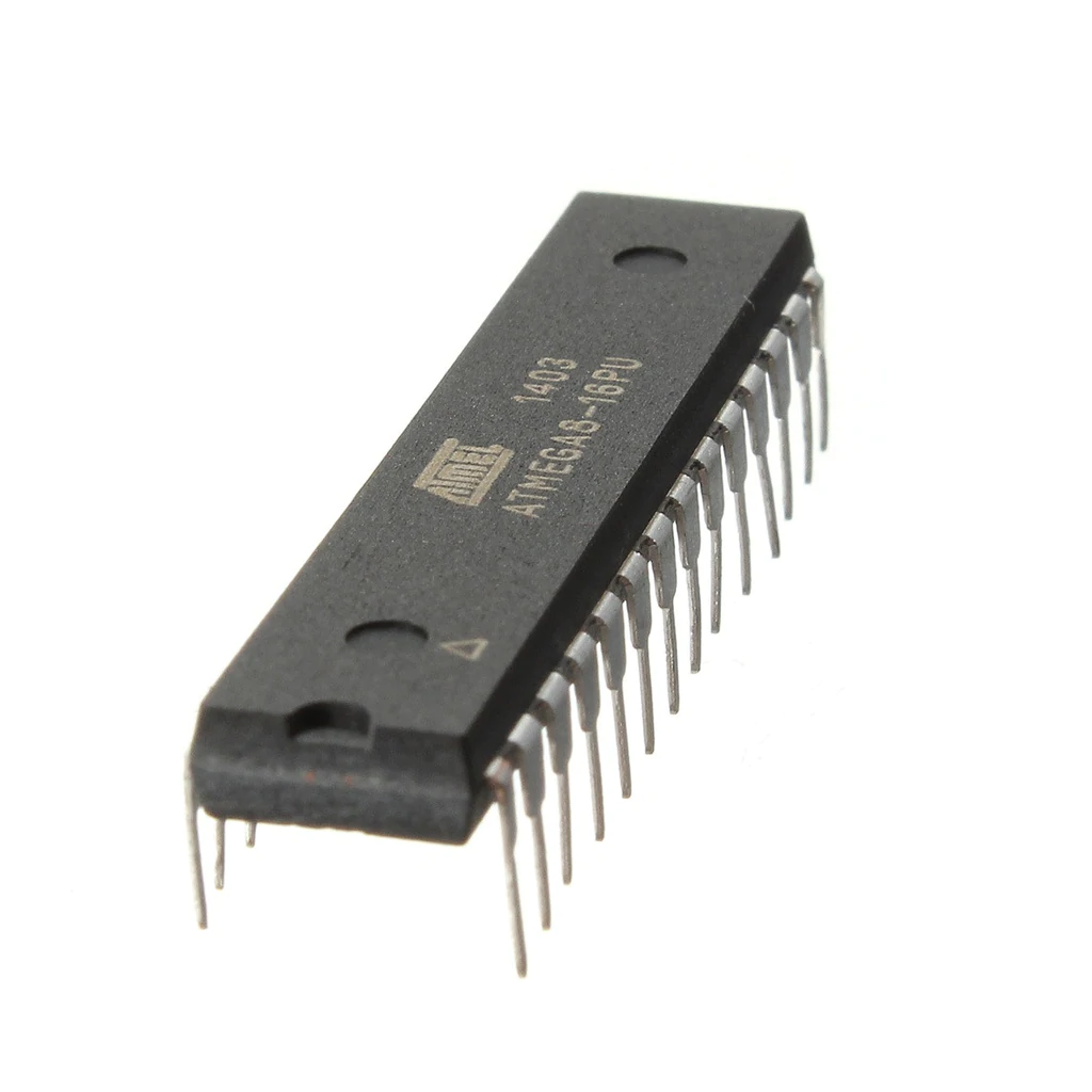
Reverse ATMEGA64 Microcomputer Flash Memory
Reverse ATMEGA64 Microcomputer Flash Memory and recover atmega64 mcu flash embedded heximal out from its flash memory and eeprom memory, read data out from microcontroller atmega64 memory;
If Interrupt Vectors are placed in the Boot Loader section and Boot Lock bit BLB02 is programmed, interrupts are disabled while executing from the Application section by breaking atmega16l locked mcu flash memory. If Interrupt Vectors are placed in the Application section and Boot Lock bit BLB12 is programed, interrupts are disabled while executing from the Boot Loader section.
The IVCE bit must be written to logic one to enable change of the IVSEL bit. IVCE is cleared by hardware four cycles after it is written or when IVSEL is written. Setting the IVCE bit will disable interrupts, as explained in the IVSEL description above.
reverter a memória flash do microcomputador ATMEGA64 e recuperar atmega64 mcu flash embutido heximal para fora de sua memória flash e memória eeprom, ler dados fora do microcontrolador atmega64 memória
All AVR ports have true Read-Modify-Write functionality when used as general digital I/O ports. This means that the direction of one port pin can be changed without unintentionally changing the direction of any other pin with the SBI and CBI instructions in order to recover protective microprocessor atmega16 firmware. The same applies when changing drive value (if configured as output) or enabling/dis- abling of pull-up resistors (if configured as input).
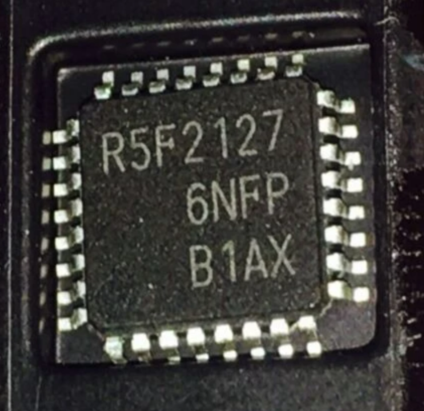
R8C R5F21276KFP Microcontroller Reverse Engineering
R8C R5F21276KFP Microcontroller Reverse Engineering will reverse mcu programming sequence and extract protected mcu r5f21276kfp source code from its memory, and then clone firmware to new microcontroller R5F21276JFP;
4 circuits: XIN clock oscillation circuit,
XCIN clock oscillation circuit (32 kHz),
High-speed on-chip oscillator (with frequency adjustment function), Low-speed on-chip oscillator
- Oscillation stop detection: XIN clock oscillation stop detection function
- Frequency divider circuit: Dividing selectable 1, 2, 4, 8, and 16
- Low power consumption modes:
Standard operating mode (high-speed clock, low-speed clock, high-speed on-chip oscillator to break R5F21292SD locked mcu flash memory, low-speed on-chip oscillator), wait mode, stop mode.
8 bits × 1 (with 8-bit prescaler)
Timer mode (period timer), pulse output mode (output level inverted every period), event counter mode, pulse width measurement mode, pulse period measurement mode.
A engenharia reversa do microcontrolador R8C R5F21276KFP reverterá a sequência de programação mcu e extrairá o código-fonte mcu r5f21276kfp protegido de sua memória e, em seguida, clonará o firmware para o novo microcontrolador R5F21276JFP
R0 is a 16-bit register for transfer, arithmetic, and logic operations. The same applies to R1 to R3. R0 can be split into high-order bits (R0H) and low-order bits (R0L) to be used separately as 8-bit data registers to attack renesas r5f21244sd microcontroller protection. R1H and R1L are analogous to R0H and R0L. R2 can be combined with R0 and used as a 32-bit data register (R2R0). R3R1 is analogous to R2R0.
Reverse ATmega8A Microchip Memory Code
Reverse ATmega8A Microchip Memory Code needs to decode atmega8a microprocessor’s tamper resistance system, then readout MCU ATmega8a firmware from its flash and eeprom memory;
There are basically two types of interrupts. The first type is triggered by an event that sets the Interrupt Flag. For these interrupts, the Program Counter is vectored to the actual Interrupt Vector in order to execute the interrupt handling routine, and hardware clears the corresponding Interrupt Flag.
Interrupt Flags can also be cleared by writing a logic one to the flag bit position(s) to be cleared. If an interrupt condition occurs while the corresponding interrupt enable bit is cleared to duplicate avr microprocessor atmega8 protected firmware, the Interrupt Flag will be set and remembered until the interrupt is enabled, or the flag is cleared by software.
recover atmega8a mcu binary file needs to break ATmega8a microprocessor fuse bit
Similarly, if one or more interrupt conditions occur while the global interrupt enable bit is cleared, the corresponding Interrupt Flag(s) will be set and remembered until the global interrupt enable bit is set, and will then be executed by order of priority.
break ATmega8A microcontroller security fuse bit and extract source code from its flash memory
The second type of interrupts will trigger as long as the interrupt condition is present. These interrupts do not nec- essarily have Interrupt Flags. If the interrupt condition disappears before the interrupt is enabled, the interrupt will not be triggered.
Reverse R5F21226DFP#U0 Microprocessor Binary Code
Reverse R5F21226DFP#U0 Microprocessor Binary Code and clone renesas mcu r5f21226dfp flash memory content to new MCU unit, original embedded firmware will be extracted from microcontroller flash memory;
3 circuits: XIN clock oscillation circuit (with on-chip feedback resistor),
On-chip oscillator (high-speed, low-speed)
(high-speed on-chip oscillator has a frequency adjustment function), XCIN clock oscillation circuit (32 kHz)
- Oscillation stop detection: XIN clock oscillation stop detection function
- Frequency divider circuit: Dividing selectable 1, 2, 4, 8, and 16
- Low power consumption modes:
Standard operating mode (high-speed clock, low-speed clock, high-speed on-chip oscillator, low-speed on-chip oscillator), wait mode, stop mode to copy locked r5f212dasn mcu flash data.
- External: 5 sources, Internal: 23 sources, Software: 4 sources
Priority levels: 7 levels
8 bits × 1 (with 8-bit prescaler)
reverso R5F21226DFP # U0 microprocessador código binário e clone renesas mcu r5f21226dfp conteúdo de memória flash para a nova unidade MCU, firmware incorporado original será extraído da memória flash microcontrolador
Timer mode (period timer), pulse output mode (output level inverted every period), event counter mode, pulse width measurement mode, pulse period measurement mode in the process of breaking ic mcu R5F2L388 firmware;
8 bits × 1 (with 8-bit prescaler)
Timer mode (period timer), programmable waveform generation mode (PWM output), programmable one-shot generation mode, programmable wait one- shot generation mode
Reverse Engineer STM32F058C8 Microprocessor Heximal
Reverse Engineer STM32F058C8 Microprocessor Heximal from its secured flash memory, the fuse bit of stm32f058c8 locked MCU will be disabled and then readout its memory program;
The device has integrated power-on reset (POR) and power-down reset (PDR) circuits. They are always active, and ensure proper operation above a threshold of 2 V to reverse engineering stm32f078r8 mcu code. The device remains in reset mode when the monitored supply voltage is below a specified threshold, VPOR/PDR, without the need for an external reset circuit.
- The POR monitors only the VDD supply voltage. During the startup phase it is required that VDDA should arrive first and be greater than or equal to VDD.
- The PDR monitors both the VDD and VDDA supply voltages, however the VDDA power supply supervisor can be disabled (by programming a dedicated Option bit) to reduce the power consumption if the application design ensures that VDDA is higher than or equal to VDD.
The device features an embedded programmable voltage detector (PVD) that monitors the VDD power supply and compares it to the VPVD threshold. An interrupt can be generated when VDD drops below the VPVD threshold and/or when VDD is higher than the VPVD threshold for the sake of recovering stm32f301r6 mcu flash memory code.
engenharia reversa STM32F058C8 microprocessador heximal de sua memória flash segura, o bit de fusível de stm32f058c8 MCU bloqueado será desativado e, em seguida, ler seu programa de memória;
The interrupt service routine can then generate a warning message and/or put the MCU into a safe state. The PVD is enabled by software.
Reverse Engineer STM32F050K4 Microprocessor
Reverse Engineer STM32F050K4 Microprocessor Protection over flash memory, and break stm32f050k4 secured mcu firmware file, extract source code from stm32f050k4 microprocessor flash memory;
The device has the following features:
- 4 Kbytes of embedded SRAM accessed (read/write) at CPU clock speed with 0 wait states and featuring embedded parity checking with exception generation for fail-critical applications by restoring microcomputer stm32f072cb firmware file.
- The non-volatile memory is divided into two arrays:
- 16 to 32 Kbytes of embedded Flash memory for programs and data
- Option bytes
- The non-volatile memory is divided into two arrays:
The option bytes are used to write-protect the memory (with 4 KB granularity) and/or readout-protect the whole memory with the following options:
- Level 0: no readout protection
- Level 1: memory readout protection, the Flash memory cannot be read from or written to if either debug features are connected or boot in RAM is selected
Level 2: chip readout protection, debug features (Cortex-M0 serial wire) and boot in RAM selection disabled.
engenharia reversa STM32F050K4 proteção do microprocessador sobre memória flash, e quebrar stm32f050k4 arquivo de firmware mcu seguro, extrair o código-fonte da memória flash do microprocessador stm32f050k4
At startup, the boot pin and boot selector option bit are used to select one of three boot options:
- Boot from User Flash
- Boot from System Memory
- Boot from embedded SRAM
The boot loader is located in System Memory. It is used to reprogram the Flash memory by using USART1.
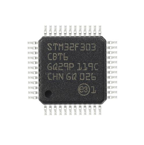
Reverse Locked STM32F303VD Flash Fuse Bit
Reverse Locked STM32F303VD Flash Fuse Bit and crack microcontroller stm32f303vd protection over the flash memory, extract embedded firmware from mcu stm32f303vd flash memory;
The ARM® Cortex®-M4 processor with FPU is the latest generation of ARM processors for embedded systems. It was developed to provide a low-cost platform that meets the needs of MCU implementation, with a reduced pin count and low-power consumption, while delivering outstanding computational performance and an advanced response to interrupts.
The ARM® Cortex®-M4 32-bit RISC processor with FPU features exceptional code-efficiency, delivering the high-performance expected from an ARM core in the memory size usually associated with 8- and 16-bit devices to ease the process of breaking microprocessor stm32f302ve flash memory.
The processor supports a set of DSP instructions which allows efficient signal processing and complex algorithm execution.
reverso bloqueado STM32F303VD flash fusível bit e crack microcontrolador stm32f303vd proteção sobre a memória flash, extrair firmware incorporado da memória flash mcu stm32f303vd
Its single precision FPU speeds up software development by using metalanguage development tools, while avoiding saturation. With its embedded ARM core, the STM32F303xD/E family is compatible with all ARM tools and software for the purpose of reverse engineering locked stm32f302re flash program.