Archive for the ‘Break IC’ Category
 Break Chip ATmega1284V Code
 January 4th, 2010 |
  Author:
 Break Chip ATmega1284V security fuse bit by crack MCU ATmega1284V tamper resistance system, extract Microcontroller code from flash memory and eeprom memory;
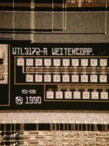
Break Chip ATmega1284V security fuse bit by crack MCU ATmega1284V tamper resistance system, extract Microcontroller code from flash memory and eeprom memory
Many register and bit references in this section are written in general form. A lower case “n” replaces the Timer/Counter number, in this case 0. A lower case “x” replaces the Output Compare Unit, in this case Compare Unit A or Compare Unit B.
However, when using the register or bit defines in a program, the precise form must be used, i.e., TCNT0 for accessing Timer/Counter0 counter value and so on. The definitions in Table 69 are also used extensively throughout the document. The Timer/Counter can be clocked by an internal or an external clock source before chip PIC16F72A binary recovery.
The clock source is selected by the Clock Select logic which is controlled by the Clock Select (CS02:0) bits located in the Timer/Counter Control Register (TCCR0B), the main part of the 8-bit Timer/Counter is the programmable bi-directional counter unit. Figure 39 shows a block diagram of the counter and its surroundings when recover IC PIC16F687 software.
Depending of the mode of operation used, the counter is cleared, incremented, or decremented at each timer clock (clkT0). ClkT0 can be generated from an external or internal clock source, selected by the Clock Select bits (CS02:0). When no clock source is selected (CS02:0 = 0) the timer is stopped. However, the TCNT0 value can be accessed by the CPU, regardless of whether clkT0 is present or not. A CPU write overrides (has priority over) all counter clear or count operations.
The counting sequence is determined by the setting of the WGM01 and WGM00 bits located in the Timer/Counter Control Register (TCCR0A) and the WGM02 bit located in the Timer/Counter Control Register B (TCCR0B). There are close connections between how the counter behaves (counts) and how waveforms are generated on the Output Compare outputs OC0A and OC0B. The Timer/Counter Overflow Flag (TOV0) is set according to the mode of operation selected by the WGM02:0 bits. TOV0 can be used for generating a CPU interrupt.
 Posted in
Break IC ATmega1284 Firmware
Break IC ATmega1284 protective system and unlock mcu atmega1284 embedded flash memory, and embedded firmware will be readout from microcontroller atmega1284;
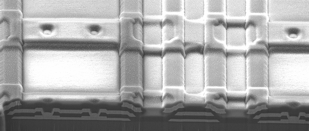
All AVR ports have true Break-Modify-Write functionality when used as general digital I/O ports. This means that the direction of one port pin can be changed without unintentionally changing the direction of any other pin with the SBI and CBI instructions when recover microcontroller stm32f105rct6 bin.
The same applies when changing drive value (if configured as output) or enabling/disabling of pull-up resistors (if configured as input). Each output buffer has symmetrical drive characteristics with both high sink and source capability. The pin driver is strong enough to drive LED displays directly.
All port pins have individually selectable pull-up resistors with a supply-voltage invariant resistance. All I/O pins have protection diodes to both VCC and Ground as indicated in Figure 33. Refer to “Electrical Characteristics” on page 367 for a complete list of parameters before break freescale mcu mc9s12xdg128.
All registers and bit references in this section are written in general form. A lower case “x” represents the numbering letter for the port, and a lower case “n” represents the bit number. However, when using the register or bit defines in a program, the precise form must be used.
For example, PORTB3 for bit no. 3 in Port B, here documented generally as PORTxn. The physical I/O Registers and bit locations are listed in “Register Description for I/O-Ports” on page 112 if break microcontroller atmega128 hex.
Three I/O memory address locations are allocated for each port, one each for the Data Register – PORTx, Data Direction Register – DDRx, and the Port Input Pins – PINx. The Port Input Pins I/O location is break only, while the Data Register and the Data Direction Register are break/write. However, writing a logic one to a bit in the PINx Register, will result in a toggle in the corresponding bit in the Data Register.
In addition, the Pull-up Disable – PUD bit in MCUCR disables the pull-up function for all pins in all ports when set. Using the I/O port as General Digital I/O is described in “Ports as General Digital I/O” on page 82. Most port pins are multiplexed with alternate functions for the peripheral features on the device.
How each alternate function interferes with the port pin is described in “Alternate Port Functions” on page 86. Refer to the individual module sections for a full description of the alternate functions.
Note that enabling the alternate function of some of the port pins does not affect the use of the other pins in the port as general digital I/O. The ports are bi-directional I/O ports with optional internal pull-ups. Figure 34 shows a functional description of one I/O-port pin, here generically called Pxn.
Each port pin consists of three register bits: DDxn, PORTxn, and PINxn. As shown in “Register Description for I/O-Ports” on page 112, the DDxn bits are accessed at the DDRx I/O address, the PORTxn bits at the PORTx I/O address, and the PINxn bits at the PINx I/O address.
The DDxn bit in the DDRx Register selects the direction of this pin. If DDxn is written logic one, Pxn is configured as an output pin. If DDxn is written logic zero, Pxn is configured as an input pin.
If PORTxn is written logic one when the pin is configured as an input pin, the pull-up resistor is activated. To switch the pull-up resistor off, PORTxn has to be written logic zero or the pin has to be configured as an output pin. The port pins are tri-stated when reset condition becomes active, even if no clocks are running.
If PORTxn is written logic one when the pin is configured as an output pin, the port pin is driven high (one). If PORTxn is written logic zero when the pin is configured as an output pin, the port pin is driven low (zero).
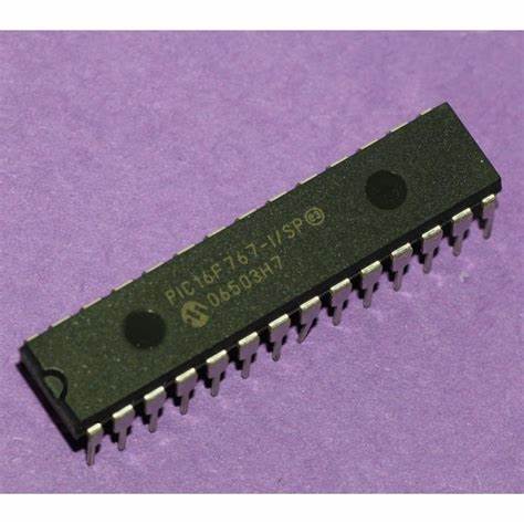
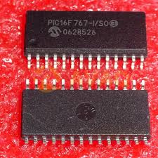
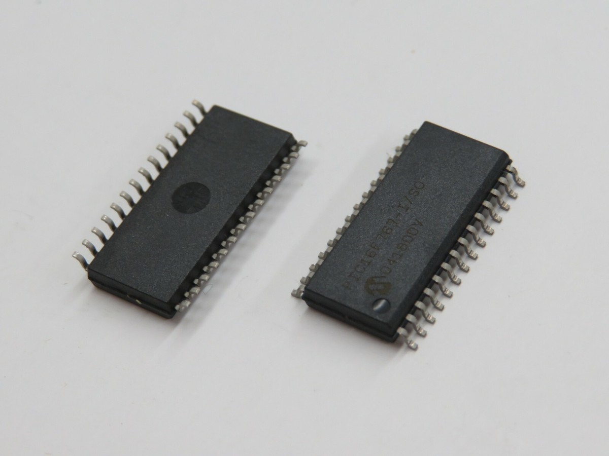
Break Microcontroller PIC16F767 Firmware
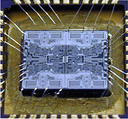
The Microchip PIC16F767 is a versatile 8-bit microcontroller (MCU) that combines analog, digital, and control features, making it an excellent choice for industrial automation, automotive electronics, consumer devices, and power management systems. With integrated EEPROM, flash memory, and multiple communication interfaces, the PIC16F767 provides a reliable platform for embedded applications. Its widespread adoption across industries makes the firmware stored inside this chip extremely valuable. However, when access to this program is lost due to security settings or damage, organizations may need to break microcontroller PIC16F767 firmware to ensure continuity of operations.
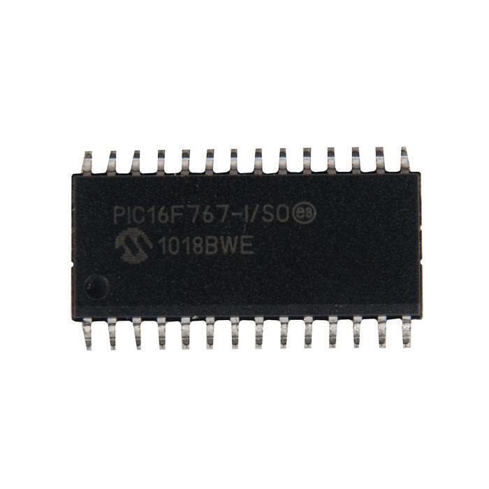
Break Microcontroller PIC16F767 protected memory include flash and eeprom area, readout embedded firmware from MCU PIC16F767 memory in the format of heximal and recover the file to blank MCU PIC16F767;
The PIC16F767 is deployed in diverse sectors thanks to its performance and cost-effectiveness:
- Industrial Control: Motor drives, PLC modules, and smart sensors often rely on the MCU for stable and efficient operation.
- Automotive Systems: Used in dashboard instruments, sensor controllers, and auxiliary power systems due to its robustness.
- Consumer Electronics: From smart appliances to portable devices, the chip manages control logic, signal processing, and user interfaces.
- Energy Management: Plays a vital role in renewable energy systems, power converters, and monitoring units.
In each of these cases, the firmware, binary files, and heximal data embedded within the flash memory of the PIC16F767 represent the heart of the system’s functionality. Losing access to this secured content can disrupt entire product lines.
Low-Power Features:
· Power-Managed modes:
– Primary Run (XT, RC oscillator, 76 µA,
1 MHz, 2V)
– RC_RUN (7 µA, 31.25 kHz, 2V)
– SEC_RUN (9 µA, 32 kHz, 2V)
– Sleep (0.1 µA, 2V)
· Timer1 Oscillator (1.8 µA, 32 kHz, 2V)
· Watchdog Timer (0.7 µA, 2V)
· Two-Speed Oscillator Start-up Oscillators:
· Three Crystal modes: – LP, XT, HS (up to 20 MHz)
· Two External RC modes
· One External Clock mode: – ECIO (up to 20 MHz)
· Internal Oscillator Block:
– 8 user-selectable frequencies (31 kHz, 125 kHz, 250 kHz, 500 kHz, 1 MHz, 2 MHz, 4 MHz, 8 MHz)
Analog Features:
· 10-bit, up to 14-channel Analog-to-Digital Converter
– Programmable Acquisition Time
– Conversion available during Sleep mode
· Dual Analog Comparators
· Programmable Low-Current Brown-out Reset (BOR) Circuitry and Programmable Low-Voltage Detect (LVD)
Peripheral Features:
· High Sink/Source Current: 25 mA
· Two 8-bit Timers with Prescaler
· Timer1/RTC module:
– 16-bit timer/counter with prescaler
– Can be incremented during Sleep via external 32 kHz watch crystal
· Master Synchronous Serial Port (MSSP) with 3-wire SPITM and I2CTM (Master and Slave) modes
· Addressable Universal Synchronous Asynchronous Receiver Transmitter (AUSART)
· Three Capture, Compare, PWM modules:
– Capture is 16-bit, max. resolution is 12.5 ns
– Compare is 16-bit, max. resolution is 200 ns
– PWM max. resolution is 10 bits
· Parallel Slave Port (PSP) – 40/44-pin devices only
Special Microcontroller Features:
· Fail-Safe Clock Monitor for protecting critical applications against crystal failure
· Two-Speed Start-up mode for immediate code execution
· Power-on Reset (POR), Power-up Timer (PWRT) and Oscillator Start-up Timer (OST)
· Programmable Code Protection
· Processor Read Access to Program Memory
· Power-Saving Sleep mode
· In-Circuit Serial Programming (ICSP) via two pins
· MPLAB® In-Circuit Debug (ICD) via two pins
· MCLR pin function replaceable with input only pin
Microchip has designed the PIC16F767 with protected memory regions and readout lock mechanisms to prevent unauthorized copying. Once enabled, these locked configurations restrict the ability to extract, dump, or readout the source code using standard tools. The main difficulties include:
- Code Protection Fuses – These permanently restrict normal access, requiring advanced techniques to unlock the data.
- Encrypted Memory Blocks – Even if partial data is obtained, it may require further processing to decrypt and decode the information.
- Tamper Resistance – Some chips can erase themselves if invasive attempts such as decapsulation or microprobing are detected.
- Data Integrity Issues – Even when recovery is possible, maintaining the original structure of the program file, EEPROM content, or firmware archive requires careful handling.
We specialize in helping clients recover and restore lost or inaccessible firmware from devices like the PIC16F767. Our expertise covers reverse engineering, controlled attack simulations, and advanced readout analysis, allowing us to extract, replicate, and duplicate essential program data without damaging the chip.
Whether your need is to copy a program, clone a working design, or retrieve critical firmware to support legacy systems, we provide a comprehensive and secure service. Our team understands the delicate nature of bypassing secured and locked MCUs and applies proven, non-destructive strategies to achieve reliable results.
Why Work With Us
- Industry-leading knowledge of Microchip PIC architecture.
- Confidential and legally compliant service for sensitive data.
- Advanced tools for safe firmware recovery and duplication.
- Proven success across automotive, industrial, and consumer applications.
When the need arises to break microcontroller PIC16F767 firmware in order to retrieve, restore, or replicate embedded files, our service offers the perfect solution. We ensure that your valuable program data can be unlocked and preserved, keeping your systems running smoothly.
Reverse IC ATmega861V Code
Reverse IC ATmega861V code programming process, disable the protective measurement by unlock microcontroller ATmega861V, extract content from MCU program memory and reprogramme the firmware to new ATmega861V;
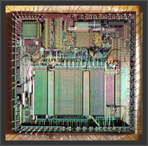
Reverse IC ATmega861V code programming process, disable the protective measurement by unlock microcontroller ATmega861V, extract content from MCU program memory and reprogramme the firmware to new ATmega861V
The Compare Output mode (COM2x1:0) bits have two functions. The Waveform Generator uses the COM2x1:0 bits for defining the Output Compare (OC2x) state at the next compare match.
Also, the COM2x1:0 bits control the OC2x pin output source. Figure 70 shows a simplified schematic of the logic affected by the COM2x1:0 bit setting. The I/O Registers, I/O bits, and I/O pins in the figure are shown in bold. Only the parts of the general I/O Port Control Registers (DDR and PORT) that are affected by the COM2x1:0 bits are shown if breaking Microcontroller PIC16C65B eeprom.
When referring to the OC2x state, the reference is for the internal OC2x Register, not the OC2x pin. The general I/O port function is overridden by the Output Compare (OC2x) from the Waveform Generator if either of the COM2x1:0 bits are set.
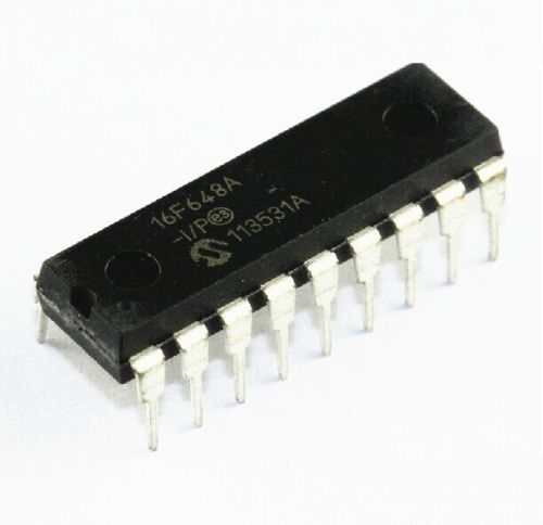
decode microprocessor PIC16F648A flash memory and extract heximal data from its memory
However, the OC2x pin direction (input or output) is still controlled by the Data Direction Register (DDR) for the port pin. The Data Direction Register bit for the OC2x pin (DDR_OC2x) must be set as output before the OC2x value is visible on the pin. The port override function is independent of the Waveform Generation mode.
The design of the Output Compare pin logic allows initialization of the OC2x state before the output is enabled. Note that some COM2x1:0 bit settings are reserved for certain modes of operation. See “8-bit Timer/Counter Register Description” on page 184 if Recover MCU PIC16F687 software code.
The Waveform Generator uses the COM2x1:0 bits differently in normal, CTC, and PWM modes. For all modes, setting the COM2x1:0 = 0 tells the Waveform Generator that no action on the OC2x Register is to be performed on the next compare match.
For compare output actions in the non-PWM modes refer to Table 88 on page 185. For fast PWM mode, refer to Table 89 on page 185, and for phase correct PWM refer to Table 90 on page 186. A change of the COM2x1:0 bits state will have effect at the first compare match after the bits are written. For non-PWM modes, the action can be forced to have immediate effect by using the FOC2x strobe bits.