Archive for the ‘Break IC’ Category
 Break IC STM32F101C4T6TR Binary
 May 13th, 2014 |
  Author:
 The STM32F101C4T6TR is a widely-used ARM Cortex-M3 based microcontroller from STMicroelectronics, known for its low power consumption and powerful real-time performance in cost-sensitive embedded systems. Frequently integrated in industrial control units, medical instruments, automotive devices, and portable electronics, this MCU often contains crucial application-specific firmware that is locked or encrypted within its secured flash memory.
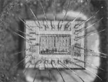
At CIRCUIT ENGINEERING CO.,LTD, we offer a highly specialized service to Break IC STM32F101C4T6TR Binary, enabling clients to gain access to protected or inaccessible firmware stored inside this chip. Whether your goal is to restore, clone, duplicate, or recover original firmware from the flash or EEPROM memory, our expert engineers are equipped with advanced tools and know-how to safely and efficiently extract the binary or heximal file.
Manufacturers often lock or encrypt the internal program memory of MCUs like the STM32F101C4T6TR to protect intellectual property or prevent unauthorized duplication. However, end-users or system integrators may require access to the original program or source code for legitimate reasons, including:
- Replacing damaged or lost firmware
- Upgrading or migrating legacy systems
- Debugging malfunctioning devices
- Performing third-party audits or system analysis
Our solution offers a reliable way to decode, decrypt, or crack these secured binaries and convert them into usable forms such as disassembled assembly listings or partial C-level reconstruction.
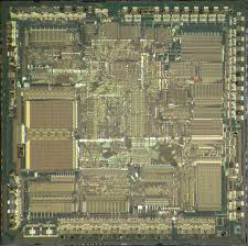
Break IC STM32F101C4T6TR memory and extract the binary or heximal out from the MCU flash and eeprom, duplicate the code to other new blank microcontroller STM32F101C4T6 which will provide the same functions;
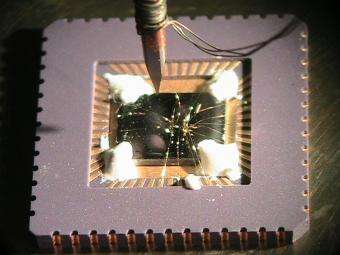
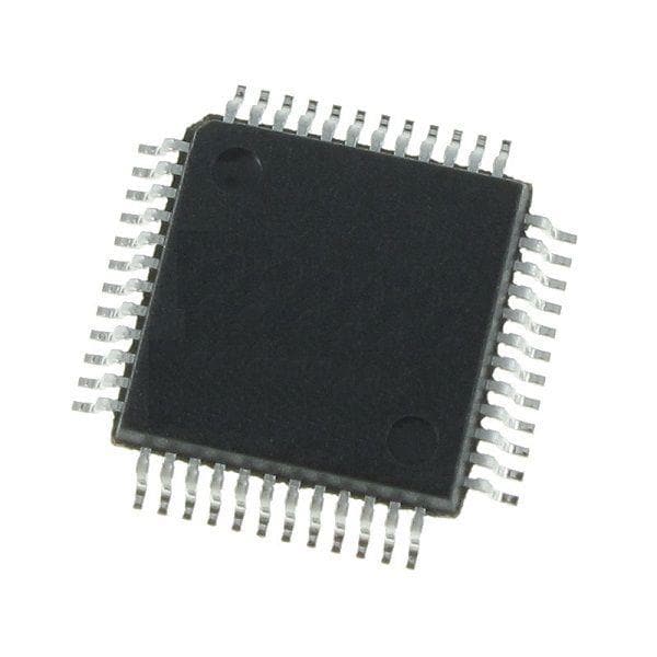
The STM32F101C4T6TR belongs to the STM32 Value Line family, offering a cost-effective solution with the following features:
- 48 MHz ARM Cortex-M3 core
- 16 KB Flash memory and 4 KB SRAM
- Multiple I/O ports, timers, USARTs, ADCs
- Power-efficient modes for battery-operated systems
- Embedded system protection features like read-out protection (ROP)
This combination makes it ideal for use in:
- Digital metering systems
- Low-power IoT sensors
- Communication gateways
- Smart controllers and industrial machinery
Unfortunately, once the read-out protection is enabled, retrieving the program from the internal flash becomes nearly impossible without expert intervention.
Features
Core: ARM 32-bit Cortex™-M3 CPU
– 36 MHz maximum frequency, 1.25 DMIPS/MHz (Dhrystone 2.1) performance at 0 wait state memory
– Single-cycle multiplication and hardware division Up to 5 timers
– Up to two16-bit timers, each with up to 4 Memories
– 16 to 32 Kbytes of Flash memory
– 4 to 6 Kbytes of SRAM Clock, reset and supply management IC/OC/PWM or pulse counter
– 2 watchdog timers (Independent and Window)
– SysTick timer: 24-bit downcounter
– 2.0 to 3.6 V application supply and I/Os
– POR, PDR and programmable voltage detector (PVD)
– 4-to-16 MHz crystal oscillator
– Internal 8 MHz factory-trimmed RC
– Internal 40 kHz RC
– PLL for CPU clock
– 32 kHz oscillator for RTC with calibration Up to 4 communication interfaces
– 1 x I2C interface (SMBus/PMBus)
– Up to 2 USARTs (ISO 7816 interface, LIN, IrDA capability, modem control)
– 1 × SPI (18 Mbit/s) CRC calculation unit, 96-bit unique ID
Device summary
– Sleep, Stop and Standby modes
– VBAT supply for RTC and backup registers
Reference
Part number
STM32F101C4, Debug mode
– Serial wire debug (SWD) and JTAG interfaces DMA
STM32F101x4
STM32F101x6
STM32F101R4,
STM32F101T4
STM32F101C6,
STM32F101R6,
STM32F101T6
– 7-channel DMA controller
– Peripherals supported: timers, ADC, SPIs, I2Cs and USARTs 1 × 12-bit, 1 µs A/D converter (up to 16 channels)
– Conversion range: 0 to 3.6 V
– Temperature sensor Up to 51 fast I/O ports
– 26/37/51 I/Os, all mappable on 16 external interrupt vectors and almost all 5 V-tolerant
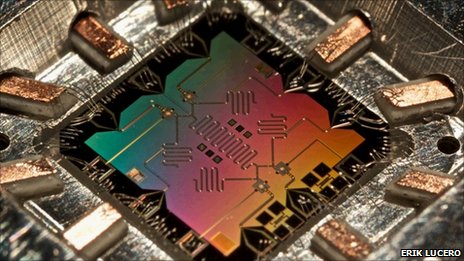
When dealing with secured, locked, or protected MCUs, our team applies a mix of hardware-based analysis, glitching techniques, and algorithmic de-obfuscation to open the firmware archive safely. We do not rely on brute force; instead, we use intelligent and precise methods to extract, copy, and analyze the content without damaging the original device.
After recovering the binary or hex file from the STM32F101C4T6TR, we can also assist with further disassembly, partial decompilation, or memory mapping to help clients understand and reuse the firmware. From EEPROM data to runtime configurations, we provide the clarity you need to replicate or restore critical system functions.
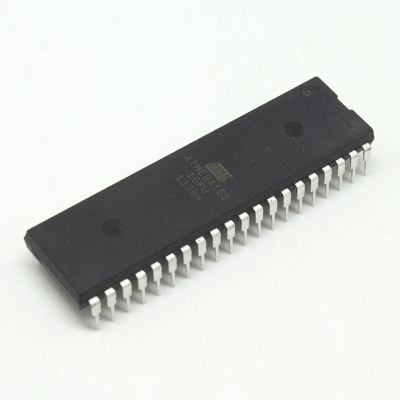
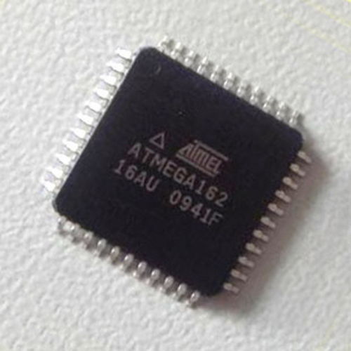
Attack MCU ATmega162 Flash
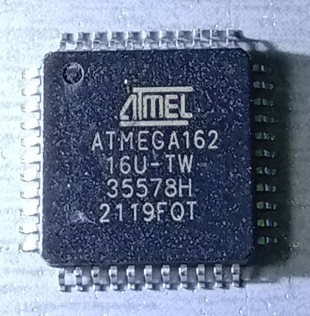
Microchip’s ATmega162 is a powerful 8-bit microcontroller often chosen for industrial, automotive, and security-critical applications due to its reliability, performance, and flexible communication features. Designed with a dual-port SRAM interface, advanced interrupt structure, and multiple USARTs, this MCU is ideal for complex embedded systems where stability and efficiency are crucial. However, its protected memory structure often presents a serious barrier for engineers, developers, or analysts who need access to the original firmware, flash, or EEPROM contents.
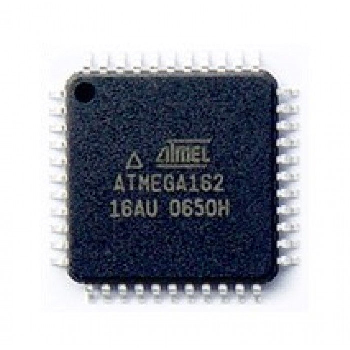
At [Your Company Name], we offer professional services to attack MCU ATmega162 flash and recover its internal heximal or binary content. Whether the target system is locked, encrypted, or has active security fuses, our experienced team applies advanced hardware and software techniques to unlock, crack, and clone the internal program data for legitimate recovery, analysis, or duplication purposes.
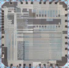
Attack MCU ATmega162 can help engineer to find out the location of security fuse bit then use laser cutting to remove it, and reset the status of Microcontroller from locked to unlocked;
Features
· High-performance, Low-power AVR® 8-bit Microcontroller
· Advanced RISC Architecture
– 131 Powerful Instructions – Most Single-clock Cycle Execution
– 32 x 8 General Purpose Working Registers
– Fully Static Operation
– Up to 16 MIPS Throughput at 16 MHz
– On-chip 2-cycle Multiplier
Non-volatile Program and Data Memories
– 16K Bytes of In-System Self-programmable Flash Endurance: 10,000 Write/Erase Cycles
– Optional Boot Code Section with Independent Lock Bits
In-System Programming by On-chip Boot Program
True Read-While-Write Operation
– 512 Bytes EEPROM
Endurance: 100,000 Write/Erase Cycles
– 1K Bytes Internal SRAM
– Up to 64K Bytes Optional External Memory Space
8-bit
Microcontroller
with 16K Bytes
In-System
– Programming Lock for Software Security
JTAG (IEEE std. 1149.1 Compliant) Interface
– Boundary-scan Capabilities According to the JTAG Standard
– Extensive On-chip Debug Support
– Programming of Flash, EEPROM, Fuses, and Lock Bits through the JTAG Interface
Peripheral Features
– Two 8-bit Timer/Counters with Separate Prescalers and Compare Modes
– Two 16-bit Timer/Counters with Separate Prescalers, Compare Modes, and
Capture Modes
– Real Time Counter with Separate Oscillator
– Six PWM Channels
– Dual Programmable Serial USARTs
– Master/Slave SPI Serial Interface
– Programmable Watchdog Timer with Separate On-chip Oscillator
– On-chip Analog Comparator
Special Microcontroller Features
– Power-on Reset and Programmable Brown-out Detection
– Internal Calibrated RC Oscillator
– External and Internal Interrupt Sources
– Five Sleep Modes: Idle, Power-save, Power-down, Standby, and Extended Standby
I/O and Packages
– 35 Programmable I/O Lines
– 40-pin PDIP, 44-lead TQFP, and 44-pad MLF
Operating Voltages
– 1.8 – 5.5V for ATmega162V
– 2.7 – 5.5V for ATmega162
Speed Grades
Programmable Flash
– 0 – 8 MHz for ATmega162V (see Figure 113 on page 265)
– 0 – 16 MHz for ATmega162 (see Figure 114 on page 265)
There are many situations where access to the firmware is essential:
- Lost original source code
- System reproduction or duplicate hardware development
- Reverse engineering for legacy support
- Decoding undocumented communication protocols
- Analyzing vulnerabilities for cybersecurity testing
The ATmega162 MCU stores its program in a flash memory block that can be fused for readout protection. Once this secured protection is activated, normal methods won’t allow developers to retrieve the original data or files. However, with our specialized capability, we can break these protective mechanisms and retrieve the internal code safely.
Our services are tailored for cases where the internal memory must be accessed due to necessity—such as system upgrades, part replacement, or system migration. We use non-invasive and semi-invasive hardware-assisted analysis to copy or clone the firmware from the embedded device.
We support:
- Full binary and hex extraction
- EEPROM and flash dump separation
- Custom bootloader readout bypass techniques
- Memory structure mapping and source code reconstruction (in C or ASM)
Once extracted, the firmware can be analyzed, decompiled, or ported to compatible systems. We also provide complete documentation of the process, allowing your engineering team to integrate or redeploy the program efficiently.
The ATmega162 is widely used in:
- Industrial controllers and HMI interfaces
- Consumer electronics with legacy serial protocols
- Secure automotive modules
- Robotics and intelligent I/O boards
- Customized smart devices using USART/SPI/I2C communication
Its dual UARTs, internal oscillator, watchdog, and flexible interrupt system make it uniquely suited for complex serial processing. Unfortunately, this also means that when firmware becomes inaccessible, the entire system may be rendered unusable—unless the memory can be restored or duplicated.
All our work is performed under strict confidentiality and aligned with legal compliance. We only provide our services for legitimate purposes such as recovery, maintenance, migration, and research—with client authorization or ownership proof required.
Conclusion
If you’re working with a locked or protected ATmega162 microcontroller and need to attack its flash to recover valuable data, CIRCUIT ENGINEERING CO., LTD is your trusted partner. Our deep expertise in reverse engineering and secure memory extraction ensures reliable access to otherwise unreachable firmware and files.
Contact us today to discuss your project and regain control over your embedded systems.
Break Chip PIC16F716 Heximal
The PIC16F716 is a compact yet powerful 8-bit microcontroller (MCU) developed by Microchip Technology, widely deployed in industrial control, home automation, and sensor-driven applications. Designed with cost efficiency and simplicity in mind, this MCU features a Flash-based program memory, internal EEPROM, analog comparators, and an integrated oscillator—all in a compact 18-pin package. While ideal for embedded systems, its protected firmware often presents challenges when data recovery or firmware duplication is necessary.

At CIRCUIT ENGINEERING CO., LTD, we specialize in offering advanced reverse engineering services to break chip PIC16F716 heximal files. This includes the ability to crack, decode, and decrypt protected program memory and EEPROM data from the chip, even when the device is secured or locked using Microchip’s code protection mechanisms.
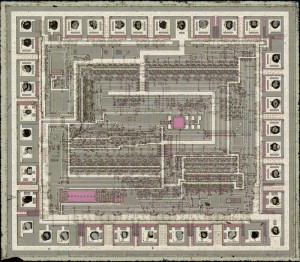
Break Chip PIC16F716 and extract Heximal out from MCU PIC16F716 flash memory, the security fuse bit of Microcontroller PIC16F716 can be removed or disable for the original MCU PIC16F716;
When clients need access to the firmware inside the PIC16F716, standard reading tools often fail due to built-in encryption and lock bits. Our team uses proprietary techniques and hardware-level exploit strategies to unlock and copy the embedded binary or heximal file from Flash or EEPROM memory. Once recovered, the data can be converted into a source code archive for analysis, debugging, or replication.

Our services cover a full range of tasks, including:
- Crack and unlock code-protected memory areas
- Restore lost or corrupted firmware from embedded devices
- Duplicate or clone firmware for hardware replacement or scale-up production
- Decrypt and decode the program file into human-readable logic
- Generate commented disassemblies or higher-level reconstructions from raw memory dumps
Microcontroller Core Features:
· High-performance RISC CPU
· Only 35 single-word instructions to learn
– All single-cycle instructions except for
program branches which are two-cycle
· Operating speed: DC – 20 MHz clock input
DC – 200 ns instruction cycle
· Interrupt capability (up to 7 internal/external interrupt sources)
· 8-level deep hardware stack
· Direct, Indirect and Relative Addressing modes
Special Microcontroller Features:
· Power-on Reset (POR)
· Power-up Timer (PWRT) and
Oscillator Start-up Timer (OST)
· Watchdog Timer (WDT) with its own on-chip RC
oscillator for reliable operation
· Dual level Brown-out Reset circuitry
– 2.5 VBOR (Typical)
– 4.0 VBOR (Typical)
· Programmable code protection
· Power-Saving Sleep mode
· Selectable oscillator options
· Fully static design
· In-Circuit Serial Programming (ICSP™)
CMOS Technology:
· Wide operating voltage range:
– Industrial: 2.0V to 5.5V
– Extended: 3.0V to 5.5V
· High Sink/Source Current 25/25 mA
· Wide temperature range:
– Industrial: -40°C to 85°C
– Extended: -40°C to 125°C
Low-Power Features:
· Standby Current:
– 100 nA @ 2.0V, typical
· Operating Current:
– 14 ìA @ 32 kHz, 2.0V, typical
– 120 ìA @ 1 MHz, 2.0V, typical
– 1 ìA @ 2.0V, typical
· Timer1 Oscillator Current:
– 3.0 ìA @ 32 kHz, 2.0V, typical
The PIC16F716 is tailored for real-time control in resource-constrained environments. With features like:

- 2K words of Flash program memory
- 128 bytes of EEPROM
- 128 bytes of RAM
- Internal 4 MHz oscillator
- Multiple analog comparators
…it is often used in low-cost embedded control applications such as:
- Home appliance control boards
- Power supplies and battery charging circuits
- Environmental monitoring and sensor hubs
- Automotive lighting and low-level control logic
This makes the PIC16F716 a prime candidate for firmware copying, especially when systems are no longer supported or require restoration after hardware failure.
Why Choose Our Reverse Engineering Solutions?
Many businesses, repair engineers, or developers face the urgent need to recover firmware from a locked, secured, or encrypted PIC16F716 chip. That’s where our deep expertise in firmware disassembly, memory analysis, and protected data extraction becomes invaluable.
We maintain strict confidentiality and legal compliance while providing efficient, low-risk firmware recovery services. Whether you’ve lost the original source files or need to duplicate a critical control board, we can extract, decrypt, and return the full heximal program archive to you in a readable format.
Peripheral Features:
· Timer0: 8-bit timer/counter with 8-bit prescaler can be incremented during Sleep via external crystal/clock
· Timer2: 8-bit timer/counter with 8-bit period register, prescaler and postscaler
· Enhanced Capture, Compare, PWM module:
– Capture is 16-bit, max. resolution is 12.5 ns
– Compare is 16-bit, max. resolution is 200 ns
– PWM maximum resolution is 10-bit
– Enhanced PWM:
– Single, Half-Bridge and Full-Bridge modes
– Digitally programmable dead-band delay
– Auto-shutdown/restart
· 8-bit multi-channel Analog-to-Digital Converter
· 13 I/O pins with individual direction control
· Programmable weak pull-ups on PORTB
Our “break chip PIC16F716 heximal” service empowers you to regain control over your embedded systems by opening up protected memory, restoring lost firmware, and enabling you to clone or copy the program data for future use. Don’t let a locked microcontroller stop your operations—contact [Your Company Name] today for professional, discrete, and highly accurate firmware recovery services tailored to your needs.
Break Microcontroller MC68376BACAB25 Program
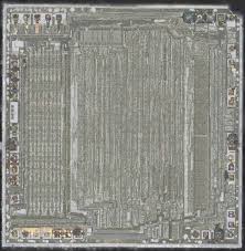
We can Break Microcontroller MC68376BACAB25 Program, please view below Microcontroller MC68376BACAB25 features for your reference:
The MC68336 and the MC68376 are highly-integrated 32-bit microcontrollers, combining high-performance data manipulation capabilities with powerful peripheral subsystems.
MC68300 microcontrollers are built up from standard modules that interface through a common intermodule bus (IMB). Standardization facilitates rapid development of devices tailored for specific applications when Break Microcontroller.
The MC68336 incorporates a 32-bit CPU (CPU32), a system integration module (SIM), a time processor unit (TPU), a configurable timer module (CTM4), a queued serial module (QSM), a 10-bit queued analog-to-digital converter module (QADC), a 3.5-Kbyte TPU emulation RAM module (TPURAM), and a 4-Kbyte standby RAM module (SRAM) if Break Microcontroller.
The MC68376 includes all of the aforementioned modules, plus a CAN 2.0B protocol controller module (TouCAN™) and an 8-Kbyte masked ROM (MRM).
The MC68336/376 can either synthesize the system clock signal from a fast reference or use an external clock input directly after Break Microcontroller. Operation with a 4.194 MHz reference frequency is standard. The maximum system clock speed is 20.97 MHz. System hardware and software allow changes in clock rate during operation. Because MCU operation is fully static, register and memory contents are not affected by clock rate changes before Break Microcontroller.
High-density complementary metal-oxide semiconductor (HCMOS) architecture makes the basic power consumption of the MCU low. Power consumption can be minimized by stopping the system clock. The CPU32 instruction set includes a low-power stop (LPSTOP) instruction that efficiently implements this capability after Break Microcontroller.
Documentation for the Modular Microcontroller Family follows the modular construction of the devices in the product line. Each microcontroller has a comprehensive user’s manual that provides sufficient information for normal operation of the device before Break Microcontroller.
The user’s manual is supplemented by module reference manuals that provide detailed information about module operation and applications. Refer to Motorola publication Advanced Microcontroller Unit (AMCU) Literature (BR1116/D) for a complete listing of documentation when Break IC.
 Posted in Break IC |
  Tags: break microcontroller encrypted archive, break microcontroller encrypted code, break microcontroller encrypted dump, break microcontroller encrypted eeprom, break microcontroller encrypted firmware, break microcontroller encrypted information, break microcontroller encrypted memory, break microcontroller encrypted program, нападам ic binary, нападам ic code, нападам ic data, нападам ic eeprom, нападам ic file, нападам ic firmware, нападам ic flash, нападам ic heximal, нападам ic memory, нападам ic program |
  Comments Closed
Break MCU MC68HC11F1CFN3 Heximal
The MC68HC11F1CFN3, a legacy 8-bit microcontroller from Freescale (formerly Motorola), has long served in automotive, industrial, and consumer electronics applications. Known for its robust performance and integrated features—including on-chip A/D converters, serial communication interfaces, and internal EEPROM—it remains embedded in critical systems even today. However, its protected memory, often secured by hardware security bits, presents a significant challenge when attempting to extract or modify the firmware for maintenance, analysis, or system upgrade.

At CIRCUIT ENGINEERING CO.,LTD, we specialize in professional microcontroller reverse engineering services. Our expertise allows us to break MCU MC68HC11F1CFN3 heximal, enabling clients to access and restore the original binary, heximal, or source code from these highly secured, locked microcontrollers.
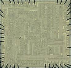
Break MCU MC68HC11F1CFN3 tamper resistance system and read heximal file out from Microcontroller MC68HC11F1, status of Microprocessor will be reset from locked to unlocked one;
Our process begins by carefully analyzing the device’s flash and EEPROM architecture. Using non-invasive and semi-invasive methods, we can crack, hack, and unlock the memory content without damaging the chip—preserving its functionality while retrieving critical data.
We extract the heximal file from the target MCU, decode the firmware, and, where necessary, decrypt encrypted sections. From there, we can help you clone or duplicate the program, convert it to a more accessible archive, or even reconstruct it into human-readable source code through disassembly or decompilation techniques.

Whether you need to copy a protected system for diagnostics or replicate functionality in a modernized platform, our service enables complete access to what was once considered inaccessible.
Features
· MC68HC11 CPU
· Power Saving STOP and WAIT Modes
· 4 Kbytes of On-Chip ROM
· 192 Bytes of On-Chip RAM (All Saved During Standby)
· 16-Bit Timer System
— 3 Input Capture (IC) Channels
— 4 Output Compare (OC) Channels
— One IC or OC Channel (Software Selectable)
· 8-Bit Pulse Accumulator
· Real-Time Interrupt Circuit
· Computer Operating Properly (COP) Watchdog System
· Synchronous Serial Peripheral Interface (SPI)
· Asynchronous Nonreturn to Zero (NRZ) Serial Communications Interface (SCI)
· 26 Input/Output (I/O) Pins
— 16 Bidirectional I/O Pins
— 3 Input Only Pins
— 3 Output Only Pins (One Output Only Pin in the 40-Pin Package)
· Available in a 44-Pin Plastic Leaded Chip Carrier (PLCC) and 40-Pin Dual In-Line Package (DIP) 2.1 VDD, VSS, and EVSS
Power is supplied to the MCU through VDD and VSS. VSS is the power supply, and VSS is ground. EVSS, available on the 44-pin PLCC, is an additional ground pin that must be grounded with VSS. The MCU operates from a single 5-volt (nominal) power supply. Very fast signal transitions occur on the MCU pins. The short rise and fall times place high, short duration current demands on the power supply. To prevent noise problems, provide good power supply bypassing at the MCU. Also, use bypass capacitors that have good high-frequency characteristics and situate them as close to the MCU as possible. Bypass requirements vary, depending on how heavily the MCU pins are loaded.

Hardware-Specific Expertise: We’re deeply familiar with the quirks and protections of the Freescale MC68HC11F1CFN3 and similar legacy devices. This means faster, safer results.
Precision and Confidentiality: We maintain strict protocols for secure data handling. All recovered firmware and files are handled with confidentiality.
End-to-End Support: We don’t just deliver raw data—we assist with interpretation, conversion, and integration into your current systems.
No Damage Guarantee: Our methods aim to preserve chip function post-extraction whenever possible, ideal for reuse or archival.
2.2 Reset (RESET)
An active low bidirectional control signal, RESET, acts as an input to initialize the MCU to a known startup state. It also acts as an open-drain output to indicate that an internal failure has been detected in either the clock monitor or COP watchdog circuit. The CPU distinguishes between internal and external reset conditions by sensing whether the reset pin rises to a logic one in less than two E-clock cycles after a reset has occurred. It is not advisable to connect an external resistor-capacitor (RC) power-up delay circuit to the reset pin of M68HC11 devices because the circuit charge time 2.3 Crystal Driver and External Clock Input (XTAL, EXTAL)
The MC68HC11F1CFN3 remains in use today due to its proven reliability in automotive control units, instrument clusters, industrial automation controllers, and legacy consumer electronics. With on-board RAM, internal EEPROM, and a flexible I/O architecture, it’s built to handle low-latency control tasks in embedded systems.
One standout feature is its bootstrap ROM, which can be leveraged for in-circuit programming or diagnostics. However, many of these features are locked down with hardware-level protection to prevent tampering or duplication—a hurdle we help you overcome.
These two pins provide the interface for either a crystal or a CMOS compatible clock to control the internal clock generator circuitry. The frequency applied to these pins is four times higher than the desired E-clock rate.
The XTAL pin is normally left unterminated when an external CMOS compatible clock input is connected to the EXTAL pin. However, a 10 kΩ to 100 kΩ load resistor connected from XTAL to ground can be used to reduce RFI noise emission. The XTAL output is normally intended to drive only a crystal. The XTAL output can be buffered with a high impedance buffer, or it can be used to drive the EXTAL input of another M68HC11.
Whether you’re tasked with maintaining a fleet of legacy control systems, duplicating a protected embedded environment, or auditing a third-party solution, our ability to break MCU MC68HC11F1CFN3 heximal and recover its firmware is your path forward. Our service is built for professionals who demand access, clarity, and reliability from even the most secured and encrypted systems.
Contact us today to learn how we can help you unlock, decode, and restore the full functionality of your Freescale MC68HC11F1CFN3-based systems.
Break IC LPC2132FBD64 Firmware
In the field of embedded electronics, the LPC2132FBD64 microcontroller—based on the ARM7TDMI-S core—is widely used in applications ranging from industrial control to medical devices and consumer electronics. With its integrated 512KB Flash memory, rich peripheral set, and advanced features, it has become a reliable choice for secure embedded system design. However, its protected and encrypted firmware often poses a significant obstacle when users need to regain access to a device’s functionality or replicate legacy systems. That’s where we come in.
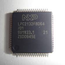
At CIRCUIT ENGINEERING CO.,LTD, we specialize in providing professional services to break IC LPC2132FBD64 firmware, allowing end users and engineers to unlock, copy, and restore the internal code of secured and locked microcontrollers. Whether it’s for product repair, legacy system recovery, or R&D, our solutions are designed to disable fuse bits, bypass read protection, and extract data securely and confidentially.
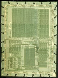
Break IC LPC2132FBD64 program memory and readout firmware from Microcontroller LPC2132FBD64, focus ion beam technique will be applied to reset the status of MCU LPC2132FBD64 from locked to unlocked one;
The LPC2132 microcontrollers are based on a 32/16 bit ARM7TDMI-S CPU with real-time emulation and embedded trace support, that combines the microcontroller with 32 kB, 64 kB, 128 kB, 256 kB and 512 kB of embedded high speed Flash memory.
Manufacturers often implement security features in microcontrollers like the LPC2132FBD64 to lock the firmware and prevent unauthorized access. While this protects intellectual property, it can become problematic for legitimate users when the original developer is unavailable, the firmware is lost, or a system needs modification. The chip’s security bits and fuse protections are intentionally designed to prevent reading of the flash, EEPROM, or memory archive, even with direct access to the device.
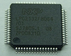
Using proprietary techniques and custom hardware interfaces, our team can carefully crack, decode, and read out the binary or heximal firmware of the LPC2132FBD64 without damaging the hardware. We also offer advanced decryption and disassembly services to convert the extracted data into readable source code or program files, enabling full analysis, reuse, or migration to other platforms.
The LPC2132FBD64 is valued for its compact 64-pin LQFP package and high-speed 60MHz CPU operation. It features two 10-bit ADCs, multiple UARTs, SPI/I2C interfaces, PWM channels, and USB 1.1 full-speed support—making it a powerful and versatile microcontroller in embedded system design. These rich peripherals are often deeply tied into the firmware, meaning that gaining access to the code is crucial for re-implementation, debugging, or custom development.
A 128-bit wide memory interface and a unique accelerator architecture enable 32-bit code execution at maximum clock rate. For critical code size applications, the alternative 16-bit Thumb mode reduces code by more than 30 % with minimal performance penalty after Copying IC PIC16F84A binary.
Our Complete Service Offering
- Firmware extraction from locked LPC2132FBD64 ICs
- Fuse bit disablement and read protection bypass
- Binary and heximal data recovery
- Conversion to C-style source code or annotated assembly
- Cloning and duplication for system replication
- Secure handling and confidential data management
Our services are trusted by electronics repair centers, product manufacturers, forensic investigators, and reverse engineering specialists. We treat each project with strict confidentiality and provide documentation of the process upon request.
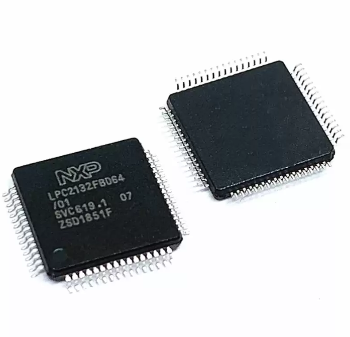
Due to their tiny size and low power consumption, these microcontrollers are ideal for applications where miniaturization is a key requirement, such as access control and point-of-sale. With a wide range of serial communications interfaces and on-chip SRAM options of 8/16/32 kB, they are very well suited for communication gateways and protocol converters, soft modems, voice recognition and low end imaging, providing both large buffer size and high processing power. Various 32-bit timers, single or dual 10-bit 8 channel ADC(s), 10-bit DAC, PWM channels and 47 GPIO lines with up to nine edge or level sensitive external interrupt pins make these microcontrollers particularly suitable for industrial control and medical systems after attacking C8051F530 firmware.
16/32-bit ARM7TDMI-S microcontroller in a tiny LQFP64 package.
8/16/32 kB of on-chip static RAM and 32/64/128/256/512 kB of on-chip Flash program memory. 128 bit wide interface/accelerator enables high speed 60 MHz operation. In-System/In-Application Programming (ISP/IAP) via on-chip boot-loader software.
Single Flash sector or full chip erase in 400 ms and programming of 256 bytes in 1 ms. EmbeddedICE RT and Embedded Trace interfaces offer real-time debugging with the on-chip RealMonitor software and high speed tracing of instruction execution.
One (LPC2132) or two (LPC2134/36/38) 8 channel 10-bit A/D converters provides a total of up to 16 analog inputs, with conversion times as low as 2.44 µs per channel. Single 10-bit D/A converter provides variable analog output (LPC2132). Two 32-bit timers/external event counters (with four capture and four compare channels each), PWM unit (six outputs) and watchdog after attack microcontroller PIC16C63A heximal.
Low power Real-time clock with independent power and dedicated 32 kHz clock input.
Multiple serial interfaces including two UARTs (16C550), two Fast I2C-bus (400 kbit/s),
SPI and SSP with buffering and variable data length capabilities.
Vectored interrupt controller with configurable priorities and vector addresses.
Up to 47 5 V tolerant general purpose I/O pins in tiny LQFP64 package.
Up to nine edge or level sensitive external interrupt pins available.
60 MHz maximum CPU clock available from programmable on-chip PLL with settling time of 100 µs.
On-chip integrated oscillator operates with external crystal in range of 1 MHz to
30 MHz and with external oscillator up to 50 MHz.
Power saving modes include Idle and Power-down
Individual enable/disable of peripheral functions as well as peripheral clock scaling down for additional power optimization.
Processor wake-up from Power-down mode via external interrupt or BOD.
Single power supply chip with POR and BOD circuits:
CPU operating voltage range of 3.0 V to 3.6 V (3.3 V ± 10 %) with 5 V tolerant I/O pads.
Attack Chip ATmega8A Binary
Microcontrollers like the ATmega8A are widely used in industrial, automotive, and consumer electronics due to their reliability and performance. However, when these chips are locked, encrypted, or protected, accessing their internal firmware, EEPROM, or flash memory becomes a difficult task. Whether you’re trying to recover legacy data, analyze a secured program, or clone a binary for backup, such protection mechanisms can be a significant obstacle. That’s where our service comes in—we specialize in attacking chip ATmega8A binary to unlock, dump, and decode the embedded content safely and professionally.
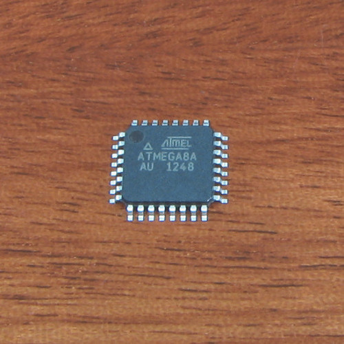
Microcontroladores como el ATmega8A son la base de innumerables sistemas embebidos, desde maquinaria industrial hasta dispositivos de consumo. Estos chips suelen almacenar lógica propietaria en forma de firmware, incrustada en la memoria flash y EEPROM interna. Para proteger la propiedad intelectual, los fabricantes habilitan funciones de seguridad que hacen ilegibles los archivos binarios internos. Pero ¿qué ocurre si el acceso es esencial, por ejemplo, para restaurar datos perdidos, copiar un programa heredado o clonar un dispositivo para mantenimiento? Ahí es donde entramos nosotros. En Circuit Engineering CO.,LTD, nos especializamos en técnicas avanzadas para atacar el binario del chip ATmega8A, lo que permite a los clientes decodificar, descifrar y extraer firmware bloqueado de microcontroladores protegidos.
Our Procedure to Attack the ATmega8A MCU
Our work involves several well-defined stages to effectively crack or clone the firmware archive locked inside a protected ATmega8A microcontroller:
1. Chip Identification and Analysis
We begin by confirming the target chip’s identity (ATmega8A) and examining its configuration. This includes analyzing fuse bits, lock bits, and memory layout to understand the level of security protection in place.
2. Non-Invasive Techniques First
Before turning to advanced methods, we test non-invasive approaches using ISP (In-System Programming) and HVPP (High-Voltage Parallel Programming). If basic access is blocked, we escalate to more complex methods.
3. Glitching and Side-Channel Attacks
In many cases, the ATmega8A uses fuse bits to disable further reading of the flash or EEPROM. We use power glitching and clock fault injection to temporarily bypass these security mechanisms. These methods target precise timing windows to trick the microcontroller into allowing memory access.
4. Dumping Embedded Memory
Once access is granted, we proceed to dump the protected EEPROM and flash memory. This includes the entire binary file, including heximal firmware and other program data stored within the chip.
5. Post-Extraction Analysis
After a successful extraction, we convert the raw dump into structured formats—such as C source code or binary files—depending on your needs. We can also help decrypt or decode proprietary formats and rebuild the firmware archive for testing or migration purposes.
6. Optional: Cloning or Duplicating
We offer a complete chip duplication service—allowing you to clone the ATmega8A firmware and write it to another identical MCU, even replicating the original protection settings if needed.
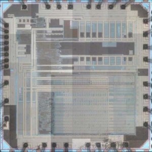
Attack Chip ATmega8A secured system, unlock microcontroller ATmega8A flash and eeprom memory, extract binary from both of the memories in the format of heximal which can be used for microcontroller copying
Attack Chip ATmega8A secured system, unlock microcontroller ATmega8A flash and eeprom memory, extract binary from both of the memories in the format of heximal which can be used for microcontroller copying;
Features
· High-performance, Low-power AVR® 8-bit Microcontroller
· Advanced RISC Architecture
– 130 Powerful Instructions – Most Single-clock Cycle Execution
– 32 x 8 General Purpose Working Registers when Chip PIC16F84A binary copying
– Fully Static Operation
– Up to 16 MIPS Throughput at 16 MHz
– On-chip 2-cycle Multiplier
High Endurance Non-volatile Memory segments
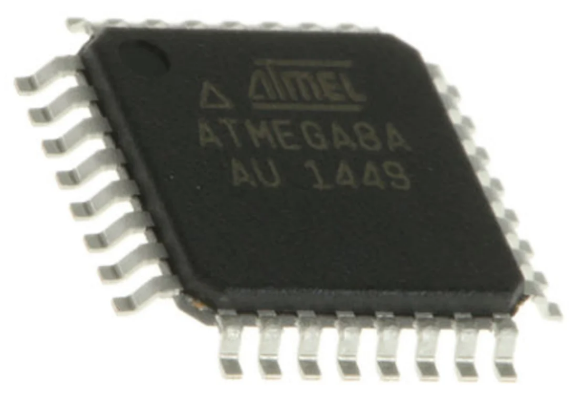
Mikrokontrolery takie jak ATmega8A są sercem niezliczonych systemów wbudowanych — od maszyn przemysłowych po urządzenia konsumenckie. Te układy często przechowują zastrzeżoną logikę w formie oprogramowania układowego, osadzonego w wewnętrznej pamięci flash i EEPROM. Aby chronić własność intelektualną, producenci włączają funkcje bezpieczeństwa, które sprawiają, że wewnętrzne pliki binarne są nieczytelne. Ale co, jeśli dostęp jest niezbędny — na przykład w celu przywrócenia utraconych danych, skopiowania starszego programu lub sklonowania urządzenia w celu konserwacji? Tutaj wkraczamy my.W Circuit Engineering CO.,LTD specjalizujemy się w zaawansowanych technikach atakowania binarnego układu ATmega8A, umożliwiając klientom dekodowanie, odszyfrowywanie i wyodrębnianie zablokowanego oprogramowania układowego z chronionych mikrokontrolerów.
– 8K Bytes of In-System Self-programmable Flash program memory
– 512 Bytes EEPROM
– 1K Byte Internal SRAM
– Write/Erase Cycles: 10,000 Flash/100,000 EEPROM
– Data retention: 20 years at 85°C/100 years at 25°C(1)
– Optional Boot Code Section with Independent Lock Bits
· In-System Programming by On-chip Boot Program
· True Read-While-Write Operation
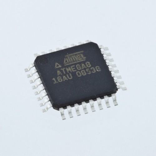
crack ATmega8A microprocessor and extract heximal code from flash memory
8-bit with 8K Bytes In-System Programmable
– Programming Lock for Software Security
Peripheral Features
– Two 8-bit Timer/Counters with Separate Prescaler, one Compare Mode
– One 16-bit Timer/Counter with Separate Prescaler, Compare Mode, and Capture Mode
– Real Time Counter with Separate Oscillator after IC C8051F530 Firmware attacking
– Three PWM Channels
– 8-channel ADC in TQFP and QFN/MLF package
· Eight Channels 10-bit Accuracy
– 6-channel ADC in PDIP package
· Six Channels 10-bit Accuracy
– Byte-oriented Two-wire Serial Interface
– Programmable Serial USART
– Master/Slave SPI Serial Interface
– Programmable Watchdog Timer with Separate On-chip Oscillator
– On-chip Analog Comparator
Special Microcontroller Features
– Power-on Reset and Programmable Brown-out Detection
– Internal Calibrated RC Oscillator
– External and Internal Interrupt Sources
– Five Sleep Modes: Idle, ADC Noise Reduction, Power-save, Power-down, and Standby
I/O and Packages
– 23 Programmable I/O Lines
– 28-lead PDIP, 32-lead TQFP, and 32-pad QFN/MLF
Operating Voltages
– 2.7 – 5.5V for ATmega8A
Speed Grades
– 0 – 16 MHz for ATmega8A
Power Consumption at 4 Mhz, 3V, 25°C
Flash ATmega8A
– Active: 3.6 mA
– Idle Mode: 1.0 mA
– Power-down Mode: 0.5 µA
Why Choose Our Service?
-
Experience with Embedded Security: We’ve helped clients across industries restore lost firmware from secured embedded systems and open protected programs blocked by manufacturers.
-
Wide Range of Tools: From logic analyzers to electromagnetic glitchers, our lab is equipped to crack secured chips with minimal risk of damage.
-
Confidential & Compliant: We treat every project with strict confidentiality and compliance, especially when dealing with proprietary or legacy systems.
-
Custom Support: Need help with just the memory dump? Or a full firmware decoding and source reconstruction? We tailor our service to your requirements.
Conclusion
If you’re facing a locked or encrypted ATmega8A and need to extract, copy, or decrypt the embedded program, we provide a proven, professional solution. From glitching protected chips to duplicating complex firmware files, we help our clients regain access and control over their embedded systems.

ATmega8A जैसे माइक्रोकंट्रोलर अनगिनत एम्बेडेड सिस्टम के दिल में हैं – औद्योगिक मशीनरी से लेकर उपभोक्ता उपकरणों तक। ये चिप्स अक्सर फ़र्मवेयर के रूप में मालिकाना तर्क संग्रहीत करते हैं, जो आंतरिक फ़्लैश और EEPROM मेमोरी के भीतर एम्बेडेड होते हैं। बौद्धिक संपदा की सुरक्षा के लिए, निर्माता सुरक्षा सुविधाएँ सक्षम करते हैं जो आंतरिक बाइनरी फ़ाइलों को अपठनीय बनाती हैं। लेकिन क्या होगा यदि पहुँच आवश्यक है – शायद खोए हुए डेटा को पुनर्स्थापित करने, विरासत प्रोग्राम की प्रतिलिपि बनाने या रखरखाव के लिए डिवाइस को क्लोन करने के लिए? यहीं पर हम आते हैं। सर्किट इंजीनियरिंग CO.,LTD में, हम चिप ATmega8A बाइनरी पर हमला करने की उन्नत तकनीकों में विशेषज्ञ हैं, जो क्लाइंट को संरक्षित माइक्रोकंट्रोलर से लॉक किए गए फ़र्मवेयर को डिकोड, डिक्रिप्ट और निकालने में सक्षम बनाता है।
Contact us to learn how we can help you attack chip ATmega8A binary and recover what’s rightfully yours—securely, efficiently, and legally.
Posted in Break IC |
Tags: атакувам mcu entsrapted bin, атакувам mcu entsrapted code, атакувам mcu entsrapted data, атакувам mcu entsrapted eeprom, атакувам mcu entsrapted file, атакувам mcu entsrapted firmware, атакувам mcu entsrapted flash, атакувам mcu entsrapted hex, атакувам mcu entsrapted memory, атакувам mcu entsrapted program |
Comments Closed
Break Microcontroller PIC18F8722 Flash
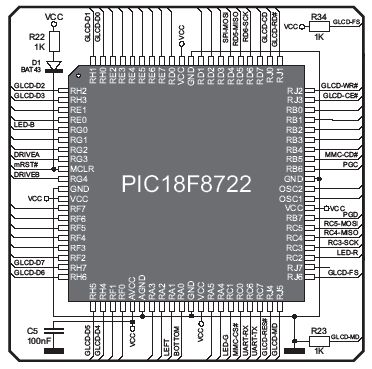
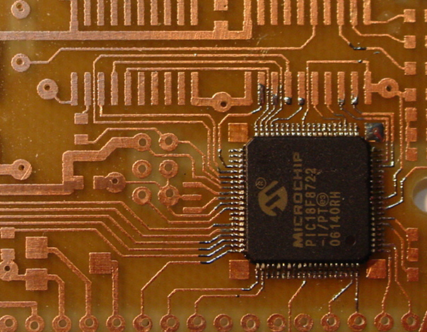
The Microchip PIC18F8722 is a powerful 8-bit microcontroller widely used in industrial control, automotive systems, and commercial embedded products due to its rich peripheral set, 128 KB of flash memory, and built-in EEPROM. Its architecture supports enhanced features like 10-bit ADC, multiple communication modules (I2C, SPI, USART), and nanoWatt technology for power efficiency, making it a popular choice for complex, secured embedded applications.
However, when this microcontroller’s flash memory becomes protected, locked, or encrypted, accessing or modifying the internal program code, firmware, or data becomes nearly impossible without the proper tools and expertise. This is where our advanced microcontroller cracking service comes in — we help clients break Microcontroller PIC18F8722 Flash and gain access to the original binary, heximal, or even high-level source code.
Our Process: How We Crack the PIC18F8722
We follow a structured and professional procedure to ensure safe and accurate recovery or duplication of protected firmware:
Однако, когда флэш-память этого микроконтроллера становится защищенной, заблокированной или зашифрованной, доступ или изменение внутреннего программного кода, прошивки или данных становится практически невозможным без соответствующих инструментов и опыта. Вот тут-то и приходит на помощь наша передовая услуга по взлому микроконтроллеров — мы помогаем клиентам взломать флэш-память микроконтроллера PIC18F8722 и получить доступ к исходному двоичному, шестнадцатеричному или даже высокоуровневому исходному коду.
Initial Assessment: We begin by analyzing the target device to determine its security fuse configuration and possible memory protection mechanisms.
Hardware Setup: Using specialized programmers and decapping or voltage glitching methods (as required), we safely unlock the microcontroller’s flash and EEPROM areas.
Dump Extraction: We copy or clone the internal firmware, data, or program files from the secured memory, even if the content is encrypted or obfuscated.
Decode & Decrypt: If the firmware archive is encoded or compressed, we decode or decrypt it using custom-built reverse engineering tools to restore human-readable formats.
Analysis & Conversion: We can optionally disassemble or decompile the binary into assembly language or reconstruct it into C source code to aid in system restoration or replication.

Break Microcontroller PIC18F8722 Flash memory tamper resistance system off, and then extract IC PIC18F8722 code from flash memory, the content can be reprogrammed to new unit for Microcontroller PIC18F8722 cloning
Break Microcontroller PIC18F8722 Flash memory tamper resistance system off, and then extract IC PIC18F8722 code from flash memory, the content can be reprogrammed to new unit for Microcontroller PIC18F8722 cloning;
Power-Managed Modes:
Peripheral Highlights (Continued):
Run: CPU on, peripherals on
Idle: CPU off, peripherals on
Sleep: CPU off, peripherals off
Idle mode currents down to 15 µA typical
Sleep current down to 0.2 µA typical
Timer1 Oscillator: 1.8 µA, 32 kHz, 2V
Watchdog Timer: 2.1 µA
Two-Speed Oscillator Start-up
quando la memoria flash di questo microcontrollore diventa protetta, bloccata o crittografata, accedere o modificare il codice di programma interno, il firmware o i dati diventa quasi impossibile senza gli strumenti e le competenze adeguate. È qui che entra in gioco il nostro servizio avanzato di cracking dei microcontrollori: aiutiamo i clienti a rompere la memoria Flash del microcontrollore PIC18F8722 e ad accedere al codice sorgente originale binario, esadecimale o persino di alto livello.
· Three Enhanced Capture/Compare/PWM (ECCP) modules
– One, two or four PWM outputs
– Selectable polarity
– Programmable dead-time
– Auto-Shutdown and Auto-Restart
· Two Master Synchronous Serial Port (MSSP) modules supporting 2/3/4-wire SPI™ (all 4 modes) and I2C™ Master and Slave modes
Flexible Oscillator Structure:
· Four Crystal modes, up to 25 MHz
· 4X Phase Lock Loop (PLL) (available for crystal and internal oscillators)
· Two External RC modes, up to 4 MHz
· Two External Clock modes, up to 40 MHz
· Internal oscillator block:
– 8 user selectable frequencies, from 31 kHz to 8 MHz
– Provides a complete range of clock speeds from 31 kHz to 32 MHz when used with PLL
– User tunable to compensate for frequency drift
· Secondary oscillator using Timer1 @ 32 kHz
· Fail-Safe Clock Monitor:
– Allows for safe shutdown if peripheral clock stops External Memory Interface (PIC18F8627/8722 only):
· Address capability of up to 2 Mbytes
· 8-bit or 16-bit interface
Peripheral Highlights:
· Two Enhanced Addressable USART modules
– Supports RS-485, RS-232 and LIN 1.2
– RS-232 operation using internal oscillator block (no external crystal required)
– Auto-wake-up on Start bit
– Auto-baud detect
· 10-bit, up to 16-channel Analog-to-Digital Converter module (A/D)
– Auto-acquisition capability
– Conversion available during Sleep
· Dual analog comparators with input multiplexing
Special Microcontroller Features:
· C compiler optimized architecture:
– Optional extended instruction set designed to optimize re-entrant code
· 100,000 erase/write cycle Enhanced Flash program memory typical
· 1,000,000 erase/write cycle Data EEPROM memory typical
· Flash/Data EEPROM Retention: 100 years typical
· Self-programmable under software control
High current sink/source 25 mA/25 mA
Four programmable external interrupts
Four input change interrupts
Two Capture/Compare/PWM (CCP) modules
· Priority levels for interrupts
· 8 X 8 Single Cycle Hardware Multiplier
· Extended Watchdog Timer (WDT):
– Programmable period from 4 ms to 131s
· Single-supply In-Circuit Serial Programming™ (ICSP™) via two pins
· In-Circuit Debug (ICD) via two pins
· Wide operating voltage range: 2.0V to 5.5V
Applications and Use Cases
Our clients come from various sectors including automotive suppliers, industrial automation firms, and OEM electronics developers. They turn to us when they need to:
Restore lost firmware after damage or manufacturer discontinuation
Duplicate or clone a working device to preserve legacy systems
Hack into their own devices to analyze vulnerabilities or perform security audits
Unlock and open protected memory to perform custom modifications or enable additional features
Why Choose Us?
Deep expertise in firmware cracking, flash memory analysis, and secured embedded systems
Strict confidentiality and security protocols for all client data
Support for converting heximal dumps into usable source code
If you’re struggling with a locked PIC18F8722 or need to recover critical data from a protected microcontroller, we’re here to help. Contact us today to learn how we can break Microcontroller PIC18F8722 Flash and unlock the full potential of your embedded systems.
Posted in Break IC |
Tags: break microcontroller embedded binary, break microcontroller embedded content, break microcontroller embedded data, break microcontroller embedded file, break microcontroller embedded flash, break microcontroller embedded heximal, break microcontroller embedded software, разбивам ic protetsted code, разбивам ic protetsted data, разбивам ic protetsted eeprom, разбивам ic protetsted file, разбивам ic protetsted firmware, разбивам ic protetsted flash, разбивам ic protetsted memory, разбивам ic protetsted program |
Comments Closed
Attack IC C8051F530 Firmware
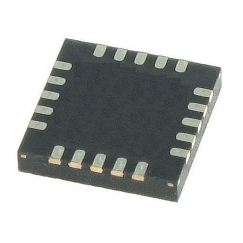
The IC C8051F530 is a powerful 8-bit microcontroller from Silicon Labs, featuring an enhanced 8051 core, integrated analog and digital peripherals, and on-chip Flash memory and EEPROM. Commonly used in industrial control systems, commercial electronics, and IoT devices, the C8051F530 is designed for embedded applications that demand reliability, low power consumption, and compact design.
O processo para atacar e clonar o firmware do C8051F530 envolve várias etapas técnicas: Identificação do Dispositivo e Configuração da Interface Começamos analisando o encapsulamento e os protocolos de comunicação do microcontrolador. O C8051F530 suporta programação no sistema por meio de sua interface C2, que acessamos usando ferramentas de hardware personalizadas. Mapeamento de Memória e Bypass de Proteção Nosso próximo passo é avaliar as configurações de proteção da memória. Muitos sistemas protegidos habilitam a proteção contra leitura de código (CRP) para impedir a extração do firmware. Aplicamos métodos não invasivos e semi-invasivos para ignorar essas proteções, dependendo da configuração do sistema. Despejando Flash e EEPROM Uma vez obtido o acesso, procedemos à cópia ou duplicação do conteúdo da memória Flash, EEPROM e outros blocos de memória. Os dados binários ou hexagonais são então armazenados em arquivos para processamento posterior.
However, the firmware stored in the Flash memory of this IC is often locked, encrypted, or otherwise protected to prevent reverse engineering or unauthorized access. This can pose challenges for engineers, security researchers, and developers who need to restore, crack, or decode the firmware for legitimate reasons—such as recovery, debugging, or system integration. At CIRCUIT ENGINEERING CO.,LTD, we specialize in services to attack IC C8051F530 firmware, helping clients unlock and extract secured system data with precision and confidentiality.
Understanding the Attack Process
The process to attack and clone the C8051F530 firmware involves several technical steps:
-
Device Identification & Interface Setup
We begin by analyzing the microcontroller’s packaging and communication protocols. The C8051F530 supports in-system programming via its C2 interface, which we tap into using custom hardware tools. -
Memory Mapping & Protection Bypass
Our next step is to assess memory protection settings. Many protected systems enable code read protection (CRP) to prevent firmware extraction. We apply non-invasive and semi-invasive methods to bypass these protections, depending on the system configuration. -
Dumping Flash & EEPROM
Once access is gained, we proceed to copy or duplicate the contents of Flash memory, EEPROM, and other memory blocks. The binary or heximal data is then dumped into files for further processing. -
Decryption & Decompilation
If the firmware is encrypted, we use advanced techniques to decrypt the data. The resulting binary is then reverse-engineered to decode the logic and convert it into C/C++ source code or assembly, depending on client needs. -
Analysis & Reconstruction
The final step involves reconstructing the program logic, analyzing the extracted firmware archive, and optionally cloning it to a new chip for duplication or emulation purposes.
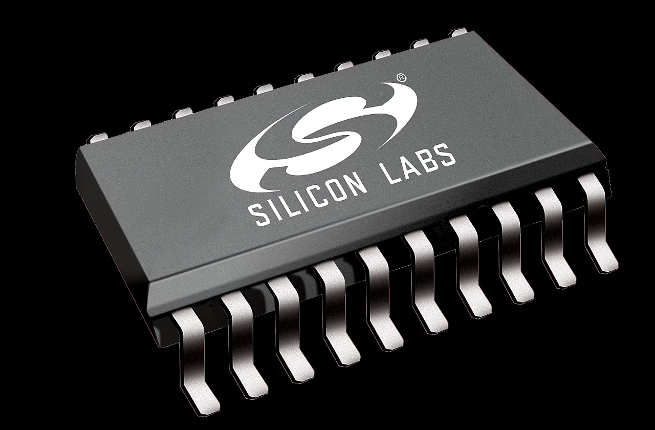
Процесс атаки и клонирования прошивки C8051F530 включает несколько технических шагов: Идентификация устройства и настройка интерфейса Мы начинаем с анализа упаковки и протоколов связи микроконтроллера. C8051F530 поддерживает внутрисистемное программирование через свой интерфейс C2, к которому мы подключаемся с помощью специальных аппаратных инструментов. Отображение памяти и обход защиты Наш следующий шаг — оценка настроек защиты памяти. Многие защищенные системы включают защиту от чтения кода (CRP) для предотвращения извлечения прошивки. Мы применяем неинвазивные и полуинвазивные методы для обхода этих защит в зависимости от конфигурации системы. Сброс Flash и EEPROM После получения доступа мы приступаем к копированию или дублированию содержимого Flash-памяти, EEPROM и других блоков памяти. Двоичные или шестнадцатеричные данные затем сбрасываются в файлы для дальнейшей обработки.
Why Clients Choose Us
-
Proven Track Record: Years of experience in firmware cracking, binary analysis, and hardware reverse engineering.
-
Tailored Services: We support a wide range of secured devices, including locked, embedded systems across multiple industries.
-
Confidentiality & Compliance: All projects are handled securely with full client confidentiality and compliance with applicable laws.
Whether you need to hack, clone, or open the source code of a C8051F530 system, our expert team is equipped to deliver efficient and ethical solutions. Contact us today to discuss how we can help you unlock your protected firmware and recover valuable program files and data archives.
Attack IC C8051F530 protective system and remove its security fuse bit, extract firmware out from MCU C8051F530 flash memory, copy heximal to blank Microcontroller C8051F530 which will provide the same functions
Attack IC C8051F530 protective system and remove its security fuse bit, extract firmware out from MCU C8051F530 flash memory, copy heximal to blank Microcontroller C8051F530 which will provide the same functions;
Analog Peripherals
– 12-Bit ADC
· ±1 LSB INL (C8051F52x/C8051F53x); no missing codes
· Programmable throughput up to 200 ksps
· Up to 6/16 external inputs
· Data dependent windowed interrupt generator
· Built-in temperature sensor
– Comparator
· Programmable hysteresis and response time
· Configurable as wake-up or reset source
· Low current
– POR/Brownout Detector
– Voltage Reference—1.5 to 2.2 V (programmable)
On-Chip Debug
– On-chip debug circuitry facilitates full-speed, non-intrusive in-system debug (No emulator required)
– Provides breakpoints, single stepping
– Inspect/modify memory and registers
– Complete development kit
Supply Voltage 2.7 to 5.25 V
– Built-in LDO regulator
High Speed 8051 µC Core
– Pipelined instruction architecture; executes 70% of instructions in 1 or 2 system clocks
– Up to 25 MIPS throughput with 25 MHz system clock
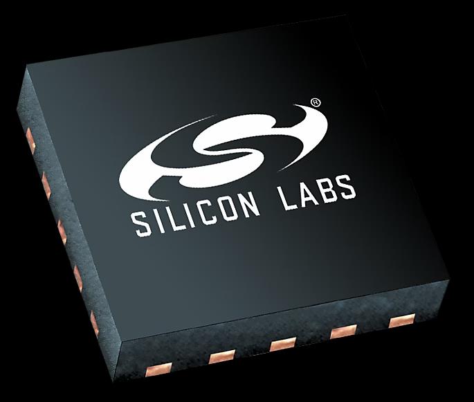
Il processo di attacco e clonazione del firmware C8051F530 prevede diverse fasi tecniche:Iniziamo analizzando il packaging e i protocolli di comunicazione del microcontrollore. Il C8051F530 supporta la programmazione in-system tramite la sua interfaccia C2, che utilizziamo utilizzando strumenti hardware personalizzati.Il nostro passo successivo consiste nel valutare le impostazioni di protezione della memoria. Molti sistemi protetti abilitano la protezione dalla lettura del codice (CRP) per impedire l’estrazione del firmware. Applichiamo metodi non invasivi e semi-invasivi per bypassare queste protezioni, a seconda della configurazione del sistema.Una volta ottenuto l’accesso, procediamo a copiare o duplicare il contenuto della memoria Flash, della EEPROM e di altri blocchi di memoria. I dati binari o esadecimali vengono quindi scaricati in file per un’ulteriore elaborazione.
Memory
– 8/4/2 kB Flash; In-system byte programmable in 512 byte sectors
– 256 bytes internal data RAM
Digital Peripherals
– 16/6 port I/O; push-pull or open-drain, 5 V tolerant
– Hardware SPI™, and UART serial port
– Hardware LIN (both master and slave, compatible with V1.3 and V2.0)
– Three general purpose 16-bit counter/timers
– Programmable 16-bit counter/timer array with three capture/compare modules, WDT
Clock Sources
– Internal oscillators: 24.5 MHz ±0.5% accuracy supports UART and LIN-Master operation
– External oscillator: Crystal, RC, C, or Clock (1 or 2 pin modes)
– Can switch between clock sources on-the-fly
Packages:
– 10-Pin QFN (3 x 3 mm)
– 20-pin QFN (4 x 4 mm)
– 20-pin TSSOP
Temperature Range: –40 to +125 °C
Posted in Break IC |
Tags: разбивам чип lotsked bin, разбивам чип lotsked data, разбивам чип lotsked eeprom, разбивам чип lotsked flash, разбивам чип lotsked hex, разбивам чип lotsked memory |
Comments Closed
Break Chip PIC16F917 Heximal
The PIC16F917 is a powerful 8-bit microcontroller by Microchip, commonly used in embedded systems for industrial control, consumer electronics, and automation products. Featuring integrated EEPROM, Flash memory, analog-to-digital converters, and a built-in LCD module driver, it supports a wide range of commercial and industrial applications. Its protective architecture includes code protection bits to prevent unauthorized access or duplication of the firmware or program data. However, there are cases where legitimate needs arise to break chip PIC16F917 heximal content for restoration, analysis, or system migration purposes.
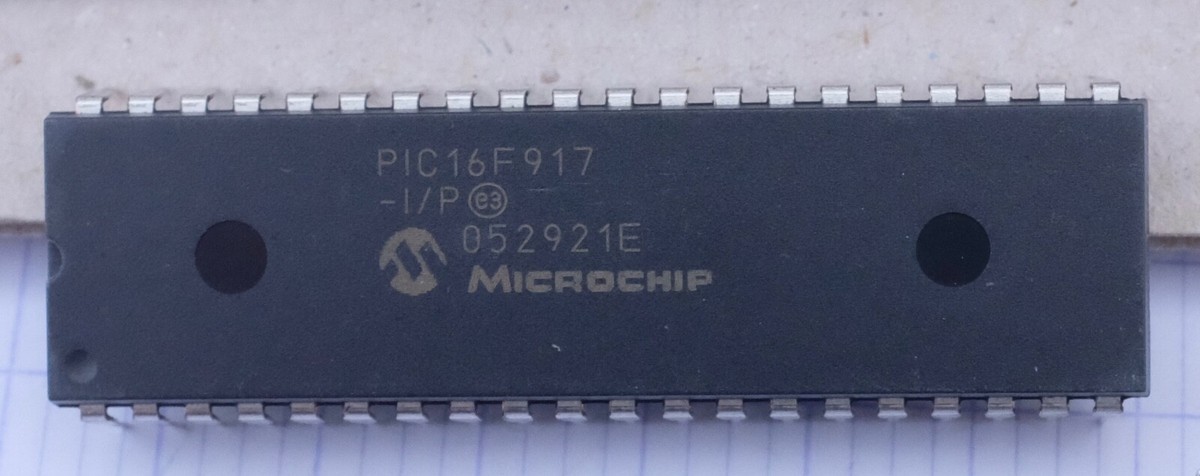
Nos especializamos en el desbloqueo, decodificación y descifrado seguro y ético de firmware heximal y binario seguro, cifrado o bloqueado de microcontroladores como el PIC16F917. Nuestra experiencia radica en eludir los mecanismos de seguridad para extraer, clonar o duplicar datos esenciales, preservando la integridad del sistema. Nuestro procedimiento comprobado para descifrar el chip PIC16F917 hexadecimal Identificación y preparación del dispositivo Comenzamos identificando el modelo del chip y leyendo su configuración. En el caso del PIC16F917, se presta especial atención al manejo de los bits de protección de código y el mapa de memoria. Configuración de la interfaz de hardware Utilizando hardware especializado ICSP (Programación en serie en circuito), establecemos comunicación con el chip de destino sin interrumpir su funcionamiento en el circuito (si es necesario).
we specialize in the secure and ethical unlocking, decoding, and decryption of secured, encrypted, or locked heximal and binary firmware from microcontrollers like the PIC16F917. Our expertise lies in bypassing security mechanisms to extract, clone, or duplicate essential data while preserving system integrity.
Our Proven Procedure to Break Chip PIC16F917 Heximal
Device Identification and Preparation
We begin by identifying the chip model and reading its configuration settings. For the PIC16F917, special care is taken to handle the code protection bits and memory map.
Hardware Interface Setup
Using specialized ICSP (In-Circuit Serial Programming) hardware, we establish communication with the target chip without disturbing its operation in the circuit (if required).
Data Access Strategy
With our custom-designed tools and methods, we crack through security layers to gain access to the flash, EEPROM, and configuration bits. Depending on the protection level, this may involve advanced techniques like glitching, fault injection, or voltage manipulation.
Firmware Dump and Analysis
Once data is accessed, we perform a complete heximal firmware dump and verify integrity. This file is then converted to readable source code through a combination of disassembly and decompilation processes.
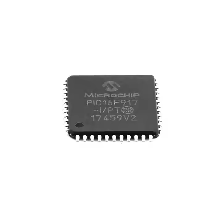
हम PIC16F917 जैसे माइक्रोकंट्रोलर से सुरक्षित, एन्क्रिप्टेड या लॉक किए गए हेक्सिमल और बाइनरी फ़र्मवेयर के सुरक्षित और नैतिक अनलॉकिंग, डिकोडिंग और डिक्रिप्शन में विशेषज्ञ हैं। हमारी विशेषज्ञता सिस्टम अखंडता को संरक्षित करते हुए आवश्यक डेटा को निकालने, क्लोन करने या डुप्लिकेट करने के लिए सुरक्षा तंत्र को बायपास करने में निहित है। चिप PIC16F917 हेक्सिमल को तोड़ने की हमारी सिद्ध प्रक्रिया डिवाइस पहचान और तैयारी हम चिप मॉडल की पहचान करके और इसकी कॉन्फ़िगरेशन सेटिंग्स को पढ़कर शुरू करते हैं। PIC16F917 के लिए, कोड सुरक्षा बिट्स और मेमोरी मैप को संभालने के लिए विशेष ध्यान रखा जाता है। हार्डवेयर इंटरफ़ेस सेटअप विशेष ICSP (इन-सर्किट सीरियल प्रोग्रामिंग) हार्डवेयर का उपयोग करके, हम सर्किट में इसके संचालन को बाधित किए बिना लक्ष्य चिप के साथ संचार स्थापित करते हैं (यदि आवश्यक हो)। डेटा एक्सेस रणनीति हमारे कस्टम-डिज़ाइन किए गए टूल और विधियों के साथ, हम फ़्लैश, EEPROM और कॉन्फ़िगरेशन बिट्स तक पहुँच प्राप्त करने के लिए सुरक्षा परतों को तोड़ते हैं। सुरक्षा स्तर के आधार पर, इसमें गड़बड़, दोष इंजेक्शन या वोल्टेज हेरफेर जैसी उन्नत तकनीकें शामिल हो सकती हैं। फ़र्मवेयर डंप और विश्लेषण एक बार डेटा एक्सेस हो जाने के बाद, हम एक पूर्ण हेक्सिमल फ़र्मवेयर डंप करते हैं और अखंडता को सत्यापित करते हैं। इस फ़ाइल को फिर डिसएसेम्बली और डीकंपाइलेशन प्रक्रियाओं के संयोजन के माध्यम से पठनीय स्रोत कोड में परिवर्तित किया जाता है।
Restoration or Duplication
The final stage involves either restoring the firmware to another device, cloning it for migration, or delivering the decoded, decrypted archive in readable format (such as C/C++ or Assembly) for further development or auditing.
Applications and Use Cases
The PIC16F917 is widely used in products like smart meters, home appliances, automotive control panels, and programmable LCD interfaces. In many cases, original firmware files may be lost or no longer supported by the manufacturer. Our service helps clients recover, unlock, and reuse these embedded systems efficiently.
Whether you need to copy, clone, or open a protected firmware, or decode a legacy program file, we provide safe, confidential solutions tailored to your technical and legal needs.
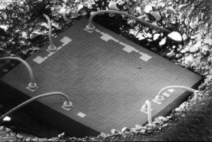
Break Chip PIC16F917 tamper resistance system and readout MCU PIC16F917 heximal from flash memory and eeprom memory, the program and data will be exactly the same as master original PIC16F917 microprocessor
Break Chip PIC16F917 tamper resistance system and readout MCU PIC16F917 heximal from flash memory and eeprom memory, the program and data will be exactly the same as master original PIC16F917 microprocessor;
High-Performance RISC CPU:
· Only 35 instructions to learn:
– All single-cycle instructions except branches
· Operating speed:
– DC – 20 MHz oscillator/clock input
– DC – 200 ns instruction cycle
· Program Memory Read (PMR) capability
· Interrupt capability
· 8-level deep hardware stack
· Direct, Indirect and Relative Addressing modes
Special Microcontroller Features:
· Precision Internal Oscillator:
– Factory calibrated to ±1%
– Software selectable frequency range of 8 MHz to 32 kHz
– Software tunable
– Two-Speed Start-up mode
– Crystal fail detect for critical applications
– Clock mode switching during operation for power savings
· Power-saving Sleep mode
· Wide operating voltage range (2.0V-5.5V)
· Industrial and Extended temperature range
· Power-on Reset (POR)
· Power-up Timer (PWRT) and Oscillator Start-up Timer (OST)
· Brown-out Reset (BOR) with software control option
· Enhanced Low-Current Watchdog Timer (WDT) with on-chip oscillator (software selectable nominal 268 seconds with full prescaler) with software enable
· Multiplexed Master Clear with pull-up/input pin
· Programmable code protection
· High-Endurance Flash/EEPROM cell:
– 100,000 write Flash endurance
– 1,000,000 write EEPROM endurance
– Flash/Data EEPROM retention: > 40 years
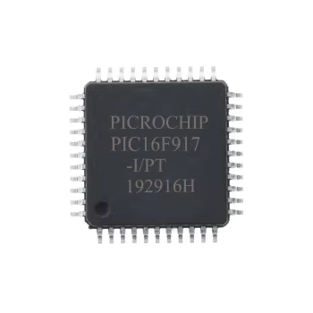
PIC16F917 gibi mikrodenetleyicilerden güvenli, şifrelenmiş veya kilitli heximal ve ikili ürün yazılımlarının güvenli ve etik bir şekilde kilidini açma, kod çözme ve şifresini çözme konusunda uzmanlaştık. Uzmanlığımız, sistem bütünlüğünü korurken temel verileri çıkarmak, klonlamak veya kopyalamak için güvenlik mekanizmalarını atlatmaktır. Çip PIC16F917 Heximal’i Kırmak İçin Kanıtlanmış Prosedürümüz Aygıt Tanımlama ve Hazırlama Çip modelini tanımlayarak ve yapılandırma ayarlarını okuyarak başlıyoruz. PIC16F917 için, kod koruma bitlerini ve bellek haritasını işlemek için özel özen gösterilir. Donanım Arayüzü Kurulumu Özel ICSP (Devre İçi Seri Programlama) donanımı kullanarak, devredeki çalışmasını bozmadan (gerekirse) hedef çip ile iletişim kurarız.
Low-Power Features:
· Standby Current:
– <100 nA @ 2.0V, typical
· Operating Current:
– 8.5 ìA @ 32 kHz, 2.0V, typical
– 100 ìA @ 1 MHz, 2.0V, typical
· Watchdog Timer Current:
– 1 ìA @ 2.0V, typical
Peripheral Features:
· Liquid Crystal Display module:
– Up to 60 pixel drive capability on 28-pin devices
– Up to 96 pixel drive capability on 40-pin devices
– Four commons
· Up to 35 I/O pins and 1 input-only pin:
– High-current source/sink for direct LED drive
– Interrupt-on-pin change
– Individually programmable weak pull-ups
· In-Circuit Serial Programming™ (ICSP™) via two pins
· Analog comparator module with:
– Two analog comparators
– Programmable on-chip voltage reference (CVREF) module (% of VDD)
– Comparator inputs and outputs externally accessible
· A/D Converter:
– 10-bit resolution and up to 8 channels
· Timer0: 8-bit timer/counter with 8-bit programmable prescaler
· Enhanced Timer1:
– 16-bit timer/counter with prescaler
– External Gate Input mode
– Option to use OSC1 and OSC2 as Timer1 oscillator if INTOSCIO or LP mode is selected
· Timer2: 8-bit timer/counter with 8-bit period register, prescaler and postscaler
· Addressable Universal Synchronous
Asynchronous Receiver Transmitter (AUSART)
· Up to 2 Capture, Compare, PWM modules:
– 16-bit Capture, max. resolution 12.5 ns
– 16-bit Compare, max. resolution 200 ns
– 10-bit PWM, max. frequency 20 kHz
· Synchronous Serial Port (SSP) with I2C™
Posted in Break IC |
Tags: разбивам микроконтролер entsrapted bin, разбивам микроконтролер entsrapted data, разбивам микроконтролер entsrapted eeprom, разбивам микроконтролер entsrapted file, разбивам микроконтролер entsrapted flash, разбивам микроконтролер entsrapted hex, разбивам микроконтролер entsrapted memory, разбивам микроконтролер entsrapted program, разбивам микроконтролер entsrapted software |
Comments Closed